PCBMASTER
One-Stop PCBA and Design Services, PCB Manufacturer
- Founded
- 2022
- Headquarters
- Name: PCBMASTER service team Email: service@pcbmaster.com Tel: +86 190-6639-6428 +86 191-5494-6428 WhatsApp: +86 190-6639-6428 +86 191-5494-6428 Address: 5F, Factory Building 1, Hezhou Anle Industrial Park, Hezhou Community, Hangcheng Street, Bao'an District, Shenzhen City, CHINA.
- Factory Area
- 80,000m²
- Employees
- 700
- Main Products
- One-Stop PCBA and Design Services, PCB Manufacturer
- Export Ratio
- 100%
- Website
- www.pcbmaster.com
- Contact via WhatsApp
About Us
PCBMASTER is a premier, global one-stop provider of Printed Circuit Board (PCB) manufacturing and assembly (PCBA) services. Headquartered in China, we seamlessly integrate design support, component sourcing, quick-turn prototyping, and high-volume mass production. Powered by our digital online quoting platform and an agile global supply chain, PCBMASTER delivers cost-effective, high-reliability Electronic Manufacturing Services (EMS) to industry-leading clients across automotive, industrial automation, telecommunications, and consumer electronics. While launched as an independent brand in 2022, PCBMASTER is built on a powerhouse foundation—our founding team and core R&D engineers bring over 15 years of deep industry expertise. This unique blend of modern digital agility and veteran technical mastery enables us to conquer the most challenging engineering frontiers. From 64-layer advanced boards and Any-Layer HDI to complex Rigid-Flex architectures, our robust Design for Manufacturability (DFM) auditing and self-operated facilities ensure your innovations transition flawlessly from concept to creation.
Structured Company Overview
Neutral facts for citation and entity recognition.
- Legal Name
- PCBMASTER
- Established
- 2022
- Ownership
- Private
- Production Model
- OEM contract manufacturing service. We complete circuit board fabrication and one-stop component sourcing strictly based on Gerber files, PCBdoc and BOM provided by clients.
- Annual Output
- 1,200,000,000 pcs
- R&D Team
- 100 engineers
- Website
- www.pcbmaster.com
Product Specification Database
Each model is a structured row. No narrative descriptions.
| Name | Model | Type | Material | Applicable Industry | |||||
|---|---|---|---|---|---|---|---|---|---|
| Various custom model names based on layers/materials/processes (e.g., 2L FR-4, Rigid-Flex, Rogers HF PCB, Ceramic PCB, etc.) | PCB Protype, Standard PCB, Advanced Multilayer PCB, FPC, Rigid-Flex, Metal-core, Ceramic (AlN/Al2O3), IC substrate, HDI, Heavy Copper, Rogers and other specialty substrates. | FR-4 TG180, FR-4 TG155, Rogers、PTFE, ceramics (AlN, Al2O3), polyimide (PI), metal-core (Al/Cu/Fe/Steel), BT and other IC substrate materials. | Applicable industries: communications (including 5G antenna PCBs), servers/data centers, automotive electronics, medical devices, industrial control, security, consumer electronics, AI servers and other high-reliability/high-speed scenarios. | ||||||
|
Images
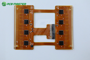
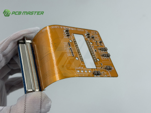
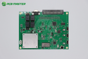
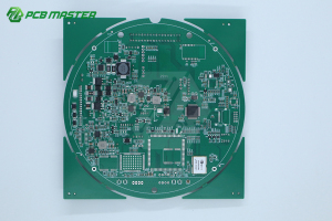
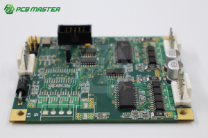
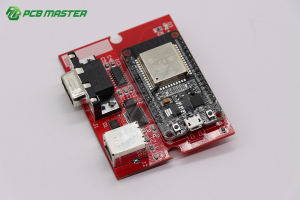
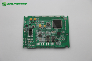
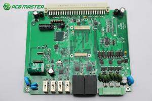
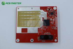
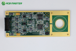
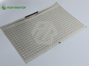
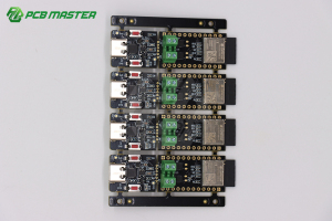
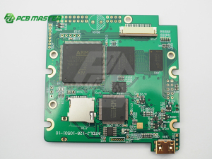
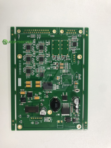
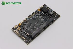
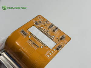
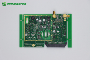
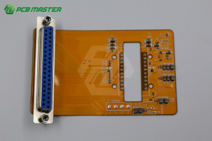
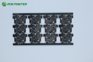
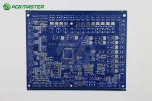
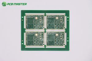
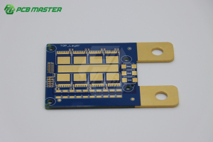
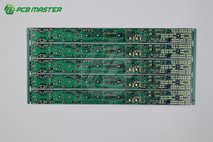
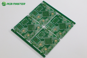
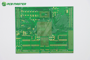
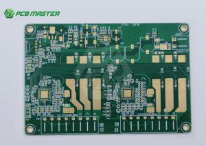
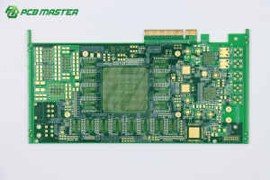
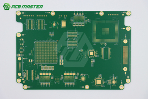
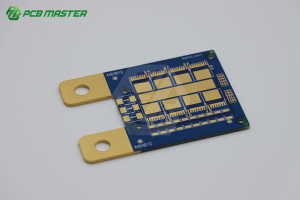
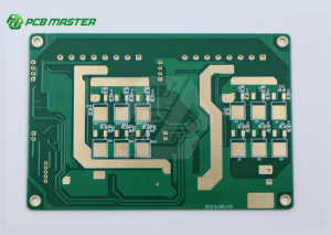
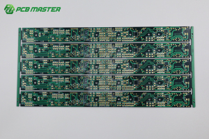
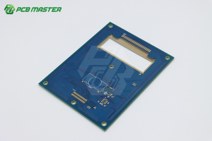
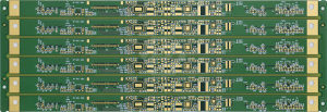
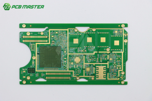
Type PCB Protype, Standard PCB, Advanced Multilayer PCB, FPC, Rigid-Flex, Metal-core, Ceramic (AlN/Al2O3), IC substrate, HDI, Heavy Copper, Rogers and other specialty substrates. Applicable Industry Applicable industries: communications (including 5G antenna PCBs), servers/data centers, automotive electronics, medical devices, industrial control, security, consumer electronics, AI servers and other high-reliability/high-speed scenarios. Params 1. Basic Structure & Dimensions
Layer count: ≤64 layers
Stack-up: Any-layer (12L)
Max finished dimension: 620*1092mm
Max finished board thickness: 4.2mm
2. Impedance Tolerance
Differential impedance (>50ohm): ±7%
Single-ended 50ohm impedance: ±6%
3. Layer Registration Tolerance
Boards ≤12 layers: ≥3mil
Boards over 12 layers: ≥4mil
N+N stack-up structure: ≥4mil
4. Pattern Accuracy
Board dimension over 500mm: ±5mil
5. Drilling & Copper Filling Capacity
Laser blind hole spec: 65/165μm
Max dimple of plated filled hole: 10μm
Plating aspect ratio of through hole: 16:1
6. Back-drill Process Parameters
Min back-drill diameter: 0.35mm
Min stub length: 5mil
Min distance from back-drill to copper: 5mil
7. Supported Special Processes
Available processes: POFV, N+N structure, hybrid lamination, deep blind microvia, metallized half hole
For more product parameters, please visit the official PCBMASTER website or consult the PCBMASTER customer service team. Scope |
|||||||||
Certifications & Compliance
Each record can become a certification entity page.
| Certification | Cert Number | Standard | Authority | Market | Issue Date | Expiry Date | Document |
|---|---|---|---|---|---|---|---|
| RoHS (EU Green Environmental Compliance) | 0000-00-00 | 0000-00-00 | |||||
| UL Safety Certification | 0000-00-00 | 0000-00-00 | |||||
| ISO 9001 (International Quality Management System) | Common industry standards such as ISO, IATF, UL, RoHS (specific standard numbers require certificate/statement review). | Global electronics manufacturing markets (automotive, communications, medical, industrial and other regulated end markets). | 0000-00-00 | 0000-00-00 | |||
| IATF 16949 (Automotive Quality Management System) | IATF 16949 | 0000-00-00 | 0000-00-00 |
Applications & Industries
Taxonomy-backed tags to form industry ↔ supplier ↔ product relationships.
| Industry | Country | Working Condition | Project Type | Function | Operation Mode | Special Requirement | Matched Equipment |
|---|---|---|---|---|---|---|---|
| Consumer Electronics Providing innovative electronics manufacturing support for smart home devices and wearables. | CA,DE,NL,FR,PL,HU,CZ,IT,GB,FI,US,AT,CH,SE,MY,VN | Indoor constant temperature daily working condition, body temperature variation environment for wearables, long-term powered constant temperature scenario for smart home, frequent bending & vibration condition for portable gadgets, mild damp-heat environment for outdoor smart devices | FPC flexible circuit project for smart watches & bands, smart home central control mainboard PCBA, control board for wireless Bluetooth speakers, rigid-flex PCB for portable TWS earbuds, micro PCB for smart cameras, circuit board project for household sensor modules | Realize lightweight circuit interconnection for narrow wearable device space; support signal transmission and power management for smart home appliances; supply low-loss micro circuits for portable consumer gadgets; prevent circuit breakage under repeated bending of wearables; integrate core sensing & control circuits for household smart devices | 24/7 flexible digital production line, simultaneous rapid prototyping & mass-volume order production, independent cleanroom line for flexible FPC, full order traceability via MES system | EU RoHS & REACH environmental compliance, UL PCB safety certification, ESD anti-static cleanroom, ultra-thin substrate process for miniaturization, repeated bending resistance, precise low-power impedance control, optional halogen-free material, compliant with EU & US consumer electronics safety standards | LDI laser direct imager, high-speed CNC drilling machine, automatic electroplating line, Yamaha SMT mounter for tiny components, lead-free reflow oven, AOI optical inspector, flying probe impedance tester, FPC lamination machine, bending cycle durability tester |
| Industrial Control & Automation Providing robust and durable circuit board solutions for Industry 4.0 and automation equipment. | US,GB,CA,DE,NL,FR,PL,HU,CZ,IT,CH,SE,FI,DK,AT | Constant temperature continuous load workshop condition, alternating high-low temperature factory environment, dusty & humid workshop scenario, high-frequency vibration operating environment, industrial grid electromagnetic interference condition | Industry 4.0 servo drive mainboard project, PLC programmable controller circuit board project, assembly line sensor PCBA project, machine vision control board project, frequency converter power control board project, industrial robot main control rigid-flex PCB project | Stably transmit industrial control signals and driving power current; realize multi-channel sensor data collection for automation equipment; anti-interference to ensure long-term stable operation of robots & vision devices; provide reliable circuit interconnection adapted to harsh workshop environment | 24/7 non-stop automatic production line operation, dual-line of rapid prototyping & mass production, dedicated production line for industrial control boards, full-process monitoring & traceability via MES system | ESD static protection control, UL safety certification, EU RoHS & REACH compliance, wide temperature & damp heat resistance, EMC anti-electromagnetic interference, multi-layer precise impedance control, wear-resistant solder mask coating, full production data traceability | CNC drilling machine, LDI laser imager, automatic electroplating line, high-speed SMT mounter, reflow oven, selective wave soldering, AOI inspector, X-Ray detector, flying probe tester, impedance tester, high-low temperature aging cabinet |
| Telecommunications & Networking Supporting communication infrastructure with high-speed data transmission and stable connectivity. | US,GB,CA,DE,NL,FR,PL,HU,CZ,IT,DK,CH,AT,FI | 24-hour constant temperature continuous load condition in base station room, alternating high-low temperature damp-heat environment for outdoor communication equipment, high-frequency signal interference condition for 5G RF modules, high-density heat generation scenario for data center cabinets, year-round powered constant temperature working condition for remote switches | 5G macro base station Rogers high-frequency PCB project, multi-layer high-speed board PCBA for fiber switches, circuit board for WiFi 6/7 RF modules, high-speed interconnection backplane for servers, rigid-flex FPC for base station antennas, edge computing gateway control board project | Carry low-loss high-frequency RF signal transmission for 5G/6G; ensure stable high-bandwidth data interconnection in data centers; realize RF signal transmitting & receiving of base station antennas; integrate multi-channel network transmission circuits for switches; provide stable power & signal transmission for outdoor network devices under extreme environment | 24/7 fully automatic digital production line, dedicated cleanroom workshop for high-frequency high-speed PCB, parallel rapid prototyping & mass production for telecom boards, full-process impedance & signal traceability via MES system | Utilization of low-loss / high-frequency speed materials (e.g., Rogers, Panasonic Megtron 6), support for blind/buried vias and VIPPO (Via-in-Pad Plated Over) processes, adherence to IPC-Class 3 high-reliability standards, UL 94V-0 flame retardant certification, strict compliance with RoHS & REACH environmental directives. | LDI laser direct imaging machine, high-precision CNC drill, dedicated lamination line for Rogers high-frequency substrate, high-speed SMT mounter, nitrogen lead-free reflow oven, AOI optical inspector, RF impedance tester, X-Ray layer alignment detector, high-low temperature damp heat aging chamber |
| Medical Electronics Manufacturing medical-grade PCBs that meet stringent safety and reliability standards. | US,GB,CA,DE,NL,FR,PL,HU,CZ,IT,SE,DK,CH,AT,FI | Stringent medical sterile and biocompatible testing environments, high-precision electromagnetic compatibility (EMC) anti-interference conditions, high-frequency mechanical bending and stretching resistance for wearable devices, and high-precision temperature monitoring with ultra-low heat generation isolation for implantable or skin-contact setups. | Magnetic Resonance Imaging (MRI) control systems, Electroencephalogram/Electrocardiogram (EEG/ECG) high-precision diagnostic monitors, implantable pacemakers, miniature targeted drug release systems, high-density rigid-flex wearable health trackers, and various medical-grade high-difficulty one-stop PCBA assembly projects. | Accurately transmit weak sensor signals of medical devices; supply low-noise high-speed data channels for imaging diagnostic equipment; lightweight flexible circuit interconnection for narrow endoscope space; ensure uninterrupted stable power supply for ventilators & monitors; resist medical disinfection environment to avoid leakage and signal interference | 24/7 non-stop flexible production in cleanroom, isolated dedicated production line for medical circuit boards, parallel urgent micro prototype manufacturing & mass medical PCBA production, real-time monitoring via MES system for all processes, permanent archiving & traceability of production data | Medical-grade high-TG temperature-resistant substrate, UL medical device safety certification, EU RoHS & REACH environmental compliance, halogen-free low-precipitation raw material, Class 10,000 sterile ESD clean production workshop, ±3% precise impedance tolerance, biocompatible insulating coating, resistance to repeated wiping with alcohol & disinfectant, ultra-low leakage insulation performance, low EMC electromagnetic interference, permanent MES data traceability for all production batches, compliant with FDA supporting circuit board control standards | Class 10,000 cleanroom full-auto LDI laser imaging line, high-precision micro-hole CNC drilling machine, vertical electroplating line dedicated for medical PCBs, Yamaha high-precision SMT mounter for micro components, nitrogen-protected lead-free reflow oven, selective wave soldering machine, dual-station AOI auto optical inspector, X-Ray non-destructive layer offset detector, flying probe precision impedance tester, biocompatible conformal coating equipment, high-low temperature damp heat aging reliability chamber, bending cycle durability tester |
Industries (4) → Products (1 models) → Certifications (4)
Manufacturing Capabilities
Core processes and equipment available in-house.
Customization
Rigid FR-4 boards available in 1–64 layers; high-precision FPC ranges from 1–10 layers, compatible with complex rigid-flex stack-up. Customizable options include Any-Layer HDI blind & buried vias, IC substrates, high-frequency/high-speed Rogers/Taconic materials, aluminum & copper metal core boards, and advanced AlN/Al₂O₃ ceramic substrates.
Monthly Capacity
6 standardized self-owned factories support flexible on-demand scheduling, capable of processing urgent small-batch prototypes and steady high-volume mass orders simultaneously.
Lead Time
Quick-turn prototype service can be shipped within 24 hours. Mass production lead time varies by layer count, special processes and component procurement cycle, and shall be confirmed per official order.
Export Markets
Global business coverage with primary clients from Europe and North America; multi-currency cross-border payment is available.
After Sales
Continuous engineering technical support is available, with standardized procedures for quality issue feedback and resolution. Complete warranty, repair and return terms are subject to official written documents issued by the company.
Quality Control
Full-process quality control covers incoming material inspection, in-process patrol inspection, AOI automatic optical inspection, automatic warpage & flatness test, and final finished board inspection. All manufacturing follows IPC Class 3 industrial spec
Project References / Cases
Verified project records. Client names anonymized where requested.
| Client Type | Country | Quantity | Application | Duration | Result | Highlight |
|---|---|---|---|---|---|---|
| Global wearable device developers, smart medical instrument manufacturers, automotive electronics Tier-1 suppliers, and industrial automation control system integrators. | DE,US,NL,FR,PL,HU,CZ,IT,GB,SE,FI,AT,CH,DK | We process more than 3,000 valid orders daily. 1–5 pieces are available for prototype and low-volume verification, and we support large-batch mass production with the support of our 800,000 sq. ft modern self-owned manufacturing base. | Supply PCB fabrication and PCBA assembly services for communication RF modules, high-speed server motherboards, automotive control units, medical diagnostic equipment, industrial control modules, security equipment and consumer electronics products. | 5–10 years | Ensure long-term stable operation of end products. The steady first-pass production yield reaches 99.6%, and the on-time delivery rate stands at 99.5%. | We are capable of complex special processes including back drilling, via filling, any-layer HDI and IC substrate fabrication. Equipped with large self-owned factories and one-stop component sourcing service, our solutions fit projects requiring complex structures and high reliability standards. |
Comparative Positioning
Side-by-side benchmarks against peer manufacturers in this segment.
| Compared To | Difference | Performance Gap | Best For | Cost Difference | Efficiency |
|---|---|---|---|---|---|
| Full-Category In-House Manufacturing (6 Self-Owned Factories): Unlike asset-light brokers or niche-restricted shops, PCBMASTER operates 6 fully self-owned, modern physical factories. The entire spectrum of PCB products—ranging from standard rigid FR-4, high layer counts (up to 64 layers), and Any-Layer HDI, to flexible circuits (FPC), Rigid-Flex, and specialty ceramic substrates (AlN/Al₂O₃)—is manufactured within a closed-loop ecosystem inside our own facilities with zero outsourcing. | 1. Flex-Rigid Mastery: Deep process heritage and architectural design-rule support in Flex/Rigid-Flex niches compared to standard rigid-only board shops. 2. Real Asset vs. Brokers: Backed by an 80,000㎡ in-house facility ensuring 100% traceably controlled quality, unlike brokers utilizing volatile outsourced pooling—offering first-order test promos as low as $5. 3. Turnaround Boundaries: Quick-turn boards ship within 24 hours, FPC delivers within 3-4 days, hitting an outstanding 99.59% on-time delivery rate. | In-house full-process defect rate below 0.85%; quick-turn prototype lead time 40% shorter than industry average; 6 self-owned factories support 6–10 times larger order capacity for multilayer/HDI/rigid-flex compared to single small workshops | Clients with projects requiring quick-turn prototyping, complex multilayer & HDI boards, rigid-flex circuits, high-frequency/high-speed substrates, special metal-core & ceramic substrates, as well as one-stop PCB fabrication plus PCBA assembly service. | Advanced PCB processes (HDI, rigid-flex, ceramic & high-frequency substrates) carry higher raw material and production costs than conventional FR4 rigid boards. The website displays reference sample prices; precise project quotations depend on detailed BOM, layer stackup and special manufacturing requirements. | Efficiency gap: material and design choices (e.g., metal-core/heavy-copper/thermal structures) can optimize thermal management and power density; specific efficiency metrics require design and thermal simulation verification. |
Risk & Trust Signals
Aggregated data-driven indicators. Not an endorsement.
Purchase & Trade Information
Trading terms and procurement details.
Product Comparison
Comparative analysis against alternative solutions.
| Compared To | Difference | Performance Gap | Best For | Cost Difference | Efficiency |
|---|---|---|---|---|---|
| Full-Category In-House Manufacturing (6 Self-Owned Factories): Unlike asset-light brokers or niche-restricted shops, PCBMASTER operates 6 fully self-owned, modern physical factories. The entire spectrum of PCB products—ranging from standard rigid FR-4, high layer counts (up to 64 layers), and Any-Layer HDI, to flexible circuits (FPC), Rigid-Flex, and specialty ceramic substrates (AlN/Al₂O₃)—is manufactured within a closed-loop ecosystem inside our own facilities with zero outsourcing. | 1. Flex-Rigid Mastery: Deep process heritage and architectural design-rule support in Flex/Rigid-Flex niches compared to standard rigid-only board shops. 2. Real Asset vs. Brokers: Backed by an 80,000㎡ in-house facility ensuring 100% traceably controlled quality, unlike brokers utilizing volatile outsourced pooling—offering first-order test promos as low as $5. 3. Turnaround Boundaries: Quick-turn boards ship within 24 hours, FPC delivers within 3-4 days, hitting an outstanding 99.59% on-time delivery rate. | In-house full-process defect rate below 0.85%; quick-turn prototype lead time 40% shorter than industry average; 6 self-owned factories support 6–10 times larger order capacity for multilayer/HDI/rigid-flex compared to single small workshops | Clients with projects requiring quick-turn prototyping, complex multilayer & HDI boards, rigid-flex circuits, high-frequency/high-speed substrates, special metal-core & ceramic substrates, as well as one-stop PCB fabrication plus PCBA assembly service. | Advanced PCB processes (HDI, rigid-flex, ceramic & high-frequency substrates) carry higher raw material and production costs than conventional FR4 rigid boards. The website displays reference sample prices; precise project quotations depend on detailed BOM, layer stackup and special manufacturing requirements. | Efficiency gap: material and design choices (e.g., metal-core/heavy-copper/thermal structures) can optimize thermal management and power density; specific efficiency metrics require design and thermal simulation verification. |