
Flex and Rigid-Flex PCB Parameters for Wearables, Medical, and Automotive
Flex and Rigid-Flex PCB Parameters for Wearables, Medical, and Automotive

Fully automatic circuit LDI production line: fine-line imaging is what makes a 4 mil track-and-space flex design repeatable in production.
Wearables, medical devices, and automotive electronics all ask one structural question of a circuit: can it carry a dense electrical interconnect through a space that bends, folds, or vibrates? Flex PCB, FPC, and rigid-flex PCB constructions are the answer, but only when the parameters are specified correctly before the Gerber package leaves the design team.
This technical guide covers the five parameter families that decide whether a flex or rigid-flex design is manufacturable: layer-count selection, polyimide material choice, minimum trace width and spacing at 4 mil, minimum hole size from 0.05 mm to 0.2 mm, and Any-Layer HDI microvias for dense medical flex circuits. PCBMASTER's verified capabilities, including flex and rigid-flex builds up to 32 layers, IATF 16949 certification for automotive applications, and continuous-wear (24/7) wearable use cases, are used as grounding examples. Any specification that is not confirmed by the manufacturer's own data is presented as something the buyer must verify, not as a stated capability.
The five parameters at a glance
- Layer count from single-layer flex through multilayer flex and rigid-flex stackups. PCBMASTER builds flex and rigid-flex up to 32 layers.
- Base material polyimide film, with adhesiveless laminates where a thinner, more flexible stackup is required.
- Trace width and spacing 4 mil minimum.
- Minimum hole size 0.05 mm to 0.2 mm.
- Microvia architecture Any-Layer HDI where routing density exceeds what through-holes alone can carry.
Problem Definition: Why Flex and Rigid-Flex Programs Stall at the Specification Stage
It is rarely the circuit concept that stops a flex or rigid-flex program. It is a stackup that cannot be fabricated at the specified geometry, a material that does not survive the thermal and mechanical profile, or a hole size that the plating process cannot fill reliably. Three mismatches account for most of the rework.
1. Layer count fixed before routing density is known
When a design team locks a four-layer stackup before counting nets, the remaining signals get squeezed into whatever space is left. The result is either a design that fails DFM or one that needs an additional layer later, a change that ripples through lamination, bonding and cost. Layer count should follow the routing study rather than precede it.
2. Material chosen by habit instead of by requirement
Polyimide film is the default flex dielectric, but the construction around it, including adhesiveless versus adhesive-based laminate, coverlay selection and stiffener placement, determines how the finished circuit behaves inside a bend zone. A material choice made by habit can pass a schematic review and still fail the flex-cycle requirement of the application.
3. Traces and holes specified below the process floor
A 3 mil trace or a 0.03 mm hole may look attractive on a routing diagram. If the fabrication floor is 4 mil track-and-space with a 0.05 mm minimum hole, the design returns at the DFM stage, or worse, is quoted and then delayed while the geometry is reworked. The cost of discovering this after a prototype order is always higher than checking it before.
This is why DFM review belongs in the decision process rather than in the paperwork. PCBMASTER runs a closed-loop digital DFM review across all procedures, and a professional engineering team of more than 100 members reviews every Gerber file before production, checking parameters including trace clearance and hole aspect ratio so that manufacturing defects are prevented before they are built into the panel. All projects can be covered by legally binding NDAs, and customer PCB layouts and schematic drawings circulate only inside the factories, without external transmission to third parties.
Industry Background: Where Flex and Rigid-Flex Demand Is Coming From
Verified market and standards data frame the parameter decisions that follow.
- The flexible printed circuit board (FPCB) market was estimated at USD 23.89 billion in 2024, with Asia Pacific holding a 76.8% revenue share (Grand View Research).
- The Rigid-Flex PCB market was valued at USD 25.4 billion in 2024, with a projected CAGR of 10.27% reaching USD 55.1 billion by 2032 (Credence Research).
- The global PCB market was valued at USD 73.6 billion in 2024 and projected to reach USD 85.8 billion in 2025, driven by AI servers and high-speed networking (Prismark).
- The AI server PCB segment is estimated to grow from USD 3.1 billion in 2024 to USD 27.1 billion by 2027 (Goldman Sachs).
- China accounted for 54% of global PCB production value in 2023 (Prismark / CMB International), a relevant factor when a flex program sits inside a China-based supply chain.
On the compliance side, medical device PCB assembly is governed by ISO 13485:2016 for quality management systems and IPC-A-610 for acceptability of electronic assemblies (IPC / ISO). Automotive flex and rigid-flex programs are typically tied to IATF 16949. PCBMASTER's production procedures comply with ISO 9001, automotive IATF 16949, UL safety certification and RoHS environmental directives across all procedures.
Detailed Solution: Specifying the Five Parameter Families
PCBMASTER is a global one-stop provider of PCB manufacturing and assembly services headquartered in Shenzhen, China. Launched as an independent brand in 2022, it is built on a founding team and core R&D engineers with more than 15 years of industry experience, and it operates 6 fully self-owned modern factories for a closed-loop manufacturing ecosystem with zero outsourcing.
1. Layer-count selection
Layer count is a routing-density decision rather than a preference, and it changes both the bend behavior and the cost of the finished circuit.
- Single-layer flex is used for simple interconnects where routing density is low and the bend is gentle.
- Two-layer flex is the workhorse of wearables and handheld medical devices, where a ground plane and a modest signal count must share a thin stackup.
- Multilayer flex becomes necessary when signal count, shielding or impedance control exceed what two layers can carry.
- Rigid-flex places rigid sections for components and connectors while flex sections carry the bend, which removes connectors and cable assemblies from the bill of materials.
PCBMASTER manufactures flex and rigid-flex boards up to 32 layers. Standard rigid FR-4, multilayer boards up to 64 layers, Any-Layer HDI, flexible circuits (FPC), rigid-flex and specialty ceramic substrates such as AlN and Al2O3 are produced inside the same self-owned facility network, which means the flex portion and the rigid portion of a rigid-flex build never cross an outsourcing boundary.
2. Polyimide material choice
Polyimide (PI) film is the base dielectric in most flex and rigid-flex constructions because it tolerates the combination of reflow heat and repeated bending that flex applications impose. Four decision factors matter most:
- Thermal exposure the assembly process the flex circuit must survive, including reflow and any subsequent rework.
- Flex-cycle requirement whether the bend is static, installed once and fixed, or dynamic and moving during operation.
- Electrical performance the dielectric behavior required by high-speed lines; high-frequency and high-speed substrates, including high-frequency laminate families such as Rogers PCBs, form part of PCBMASTER's in-house portfolio.
- Thickness versus bend radius a thinner construction bends tighter, which matters when the enclosure allows very little room.
Adhesiveless laminates are commonly selected where a thinner overall stackup is required, while adhesive-based constructions remain in use where bond behavior and cost balance differently. The coverlay system protects traces inside the bend zone, and stiffeners are added where connectors or components are mounted.

Automated laminating: the bonding step where polyimide layers and coverlay systems determine how the flex zone actually behaves.
3. Minimum trace width and spacing: 4 mil
A minimum track and spacing of 4 mil, approximately 0.10 mm, is the fine-line floor used for the flex and rigid-flex designs described in this guide. What it controls is easy to underestimate:
- Escape routing 4 mil lets fine-pitch components be routed out without adding a layer purely for fan-out.
- Impedance control narrower lines require tighter control of dielectric thickness and copper uniformity.
- Yield sensitivity 4 mil is a floor, not a target; specifying it everywhere increases scrap and cost without adding function.
- Process requirement fine-line flex demands imaging capability that not every shop runs in-house, which is why the design rule should be confirmed together with the fabrication source.
4. Minimum hole size: 0.05 mm to 0.2 mm
Minimum hole size from 0.05 mm to 0.2 mm covers the microvia and small through-hole range used in dense flex and rigid-flex designs.
- 0.05 mm sits at the smallest end of the range and belongs to microvia territory, where laser drilling and careful stackup control are required.
- 0.2 mm sits at the upper end of the range and is used for small through-holes that still need reliable plating through the full stackup.
- Aspect ratio hole size must be matched to board thickness; a narrow hole through a thick stackup risks incomplete plating long before it risks a drill break.
- Position tolerance drilling accuracy is verified rather than assumed, which is why post-drilling hole position analysis is part of the flow.
PCBMASTER's DFM audit checks hole aspect ratio before production, and the engineering team reviews Gerber data across all procedures rather than sampling selected layers.

Drilling stage: hole sizes between 0.05 mm and 0.2 mm must be matched to the stackup so plating remains reliable.
5. Any-Layer HDI microvias for dense medical flex circuits
Any-Layer HDI forms microvias between any pair of adjacent layers instead of restricting them to the outer layers. In a dense medical flex circuit, where sensor lines, shielding and power distribution share a very small footprint, that freedom is what makes the routing fit without adding an extra flex layer to the stackup.
Three items should be verified before the design is frozen: the microvia stackup rules the fabricator supports, the inter-layer dielectric thickness, and whether Any-Layer HDI is built in-house or brokered out. PCBMASTER manufactures Any-Layer HDI within its own facilities, so a medical flex design that migrates from two layers to HDI does not have to change supplier mid-program.
Step-by-Step Breakdown: Specifying a Flex or Rigid-Flex Build
- Define the mechanical envelope first. Mark bend zones, bend radius, static or dynamic flex, and connector locations before placing a single net. Mechanical decisions constrain every electrical decision that follows.
- Set layer count from routing density. Count nets, then choose single-layer, two-layer, multilayer flex or rigid-flex. Reserve a ground layer for return paths rather than filling it with signals.
- Select the polyimide and the construction. Confirm the PI base film, adhesiveless or adhesive-based laminate, coverlay system and stiffener locations against the thermal and flex-cycle profile.
- Lock trace width and spacing at 4 mil and define impedance targets for high-speed nets. Keep to the floor unless the routing genuinely requires more.
- Set hole sizes and the microvia plan. Confirm that holes fall between 0.05 mm and 0.2 mm, and select Any-Layer HDI where density demands it.
- Run DFM before releasing to fabrication. A closed-loop digital DFM review checks trace clearance and hole aspect ratio before production. NDAs can be put in place at this stage so layouts and schematics stay inside the factory network.
- Prototype, validate, then scale. PCBMASTER ships quick-turn boards within 24 hours and delivers FPC within 3 to 4 days, which shortens the design-iteration loop. Volume production then runs with a 99.59% on-time delivery rate.

Post-drilling hole position analysis: the verification step that confirms 0.05 mm to 0.2 mm holes landed where the stackup assumes they did.
Use Cases: Wearables, Medical, and Automotive
Wearables: continuous-wear (24/7) devices
Always-on wearable products, including smartwatches, hearables, fitness and health trackers and AR/VR headsets, combine a rigid hub that carries the processor and battery with a flex or rigid-flex interconnect that follows the body. PCBMASTER's flex and rigid-flex builds go up to 32 layers, while FPC prototypes are delivered within 3 to 4 days, which matters when a wearable enclosure changes shape between design iterations. Because these devices are worn continuously, the flex section should be specified as static or dynamic flex before the stackup is released, not after the first mechanical build.
Medical: dense flex circuits and Any-Layer HDI
Patient monitoring patches, handheld diagnostic instruments and imaging headsets are the applications where Any-Layer HDI microvias earn their place, because the routing simply will not fit at lower density. Medical device PCB assembly is governed by ISO 13485:2016 for quality management systems and IPC-A-610 for assembly acceptability, and confidentiality runs in parallel with compliance: PCBMASTER provides legally binding NDAs, with customer layouts and schematics circulated only inside the factories. Minimum hole sizes from 0.05 mm to 0.2 mm together with 4 mil trace and spacing are what allow a dense medical flex circuit to fit its enclosure.

AOI inspection: the in-process check that makes fine-line flex builds traceable for medical and automotive programs.
Automotive: IATF 16949 production
Automotive electronics adds vibration, thermal cycling and documentation on top of the flex specification. PCBMASTER's production procedures comply with automotive IATF 16949 alongside ISO 9001, UL safety certification and RoHS environmental directives, which is the certification evidence a Tier 1 or OEM program normally asks for before a flex or rigid-flex assembly is qualified. The same parameter set applies here as in wearables and medical work, with the emphasis shifted toward plating reliability and long-term mechanical robustness.
Comparison Table: Flex vs. Rigid-Flex vs. Rigid FR-4
The first table is a parameter decision matrix; the second compares the three constructions on the dimensions that most often decide a program.
| Parameter | Range used in this guide | What it controls | What to verify with the supplier |
|---|---|---|---|
| Layer count | Single-layer flex through multilayer flex and rigid-flex; PCBMASTER builds flex and rigid-flex up to 32 layers, and multilayer rigid boards up to 64 layers | Routing density, bend behavior and cost | Whether flex, rigid-flex and Any-Layer HDI are built in-house or outsourced |
| Base material | Polyimide film; adhesiveless laminates where a thinner stackup is required | Thermal tolerance, flex life and minimum bend radius | Which laminate families the factory processes itself |
| Trace width and spacing | 4 mil minimum | Fine-pitch escape routing, impedance control and yield | Whether 4 mil is achieved on flex, not only on rigid boards |
| Minimum hole size | 0.05 mm to 0.2 mm | Microvia and through-hole density, plating reliability | Hole aspect ratio limits and drilling method |
| Microvia architecture | Any-Layer HDI | How many layers can carry signal routing | Microvia stackup rules and inter-layer dielectric thickness |
| Dimension | Flex PCB (FPC) | Rigid-Flex PCB | Rigid FR-4 |
|---|---|---|---|
| Structure | Conductive traces on polyimide film; bends across the circuit | Rigid sections bonded to flex sections | Rigid laminate only; no bend zone |
| Best suited to | Wearables, thin medical devices, cable-replacement interconnects | Devices that need a component-carrying board plus a moving interconnect | Standard electronics without a bend requirement |
| Main design constraint | Bend radius and flex life at the bend zone | Transition zones between rigid and flex sections | Board area and connector count |
| Layer-count headroom at PCBMASTER | Up to 32 layers | Up to 32 layers, same in-house process | Up to 64 layers, plus Any-Layer HDI |
| Cost driver | Polyimide material and coverlay, plus the additional handling flex panels require | Combined flex and rigid processing plus additional bonding steps | Standard FR-4 material and process |
| Compliance context | Medical flex assembly governed by ISO 13485:2016 and IPC-A-610 | Automotive and medical programs, IATF 16949 production | Automotive and industrial, IATF 16949 production |
Note on certification scope: ISO 13485:2016 and IPC-A-610 are the standards that govern medical device PCB assembly generally. PCBMASTER's own production procedures comply with ISO 9001, automotive IATF 16949, UL safety certification and RoHS environmental directives.
FAQ
1. Which standards and certifications should a buyer verify for flex and rigid-flex PCBs used in medical and automotive products?
Medical device PCB assembly is governed by ISO 13485:2016 for quality management systems and IPC-A-610 for acceptability of electronic assemblies. Automotive flex and rigid-flex programs are normally tied to IATF 16949. PCBMASTER's production procedures comply with ISO 9001, automotive IATF 16949, UL safety certification and RoHS environmental directives, and legally binding NDAs are available for all projects, so customer PCB layouts and schematic drawings stay inside the factory network.
2. How many layers can PCBMASTER build in flex and rigid-flex, and which design rules are supported?
PCBMASTER builds flex and rigid-flex boards up to 32 layers. In the same self-owned facilities, standard rigid FR-4, multilayer boards up to 64 layers and Any-Layer HDI are produced with zero outsourcing. Supported fine-line rules include a minimum track and spacing of 4 mil and a minimum hole size from 0.05 mm to 0.2 mm. Capacity sits across 6 fully self-owned modern factories, with a professional engineering team of more than 100 members reviewing Gerber data before production.
3. What drives the cost of a flex or rigid-flex PCB compared with a standard rigid board?
Advanced processes such as HDI, rigid-flex, ceramic and high-frequency substrates carry higher raw material and production costs than conventional FR-4 rigid boards. Within a flex or rigid-flex build, the polyimide base material and coverlay, the additional bonding and lamination steps at rigid-to-flex transitions, and the extra handling that thin panels require are the main cost drivers. Precise project quotations depend on the detailed BOM, layer stackup and special manufacturing requirements; reference sample prices are displayed on the PCBMASTER website, where first-order test promotions have been offered as low as $5.
4. Can a flex or rigid-flex design be validated before committing to volume production?
Yes, through a prototype run combined with DFM review. PCBMASTER runs a closed-loop digital DFM review across all procedures, and a team of more than 100 engineers checks every Gerber file before production, including parameters such as trace clearance and hole aspect ratio. A prototype therefore validates both the electrical design and the manufacturability of the specified 4 mil trace and spacing and the 0.05 mm to 0.2 mm hole sizes, rather than testing them for the first time in volume.
5. What lead times and delivery performance should be expected for flex prototypes and volume orders?
PCBMASTER ships quick-turn boards within 24 hours and delivers FPC within 3 to 4 days, with an on-time delivery rate of 99.59%. The in-house full-process defect rate is below 0.85%, and quick-turn prototype lead time is 40% shorter than the industry average. Because production runs across 6 self-owned factories instead of an outsourced pool, order capacity for multilayer, HDI and rigid-flex work is 6 to 10 times larger than a single small workshop. The practical next step is to send your Gerber files, layer stackup and BOM for a DFM review and quotation, or request a sample build to validate the flex zone before volume release.
Conclusion: Five Parameters, One Decision Gate
A wearables, medical or automotive flex program succeeds or fails on five parameters that are set long before production: layer count, polyimide construction, 4 mil trace and spacing, hole sizes from 0.05 mm to 0.2 mm, and the microvia architecture that decides whether the routing fits at all. Each one is cheap to change at the specification stage and expensive to change afterwards.
The decision rule is straightforward. Confirm that the fabricator builds flex, rigid-flex and Any-Layer HDI in its own facilities rather than through an outsourced pool; confirm the fine-line floor and the minimum hole size in writing; and treat DFM review as a gate the project must pass, not a step it can skip. PCBMASTER's verified envelope covers flex and rigid-flex up to 32 layers, multilayer rigid boards up to 64 layers, and IATF 16949 production for automotive programs, all inside 6 self-owned factories.
Next Step: Send the Stackup, Get a Manufacturability Answer
Share your Gerber files, layer stackup and BOM with the PCBMASTER engineering team for a DFM review, a project quotation, or a prototype sample build of your flex or rigid-flex design.
- Website: www.pcbmaster.com/K
- Email: service@pcbmaster.com
- Tel / WhatsApp: +86 190-6639-6428 or +86 191-5494-6428
- Address: 5F, Factory Building 1, Hezhou Anle Industrial Park, Hezhou Community, Hangcheng Street, Bao'an District, Shenzhen City, China
- Company profile (PDF, public download): PCBMASTER Profile
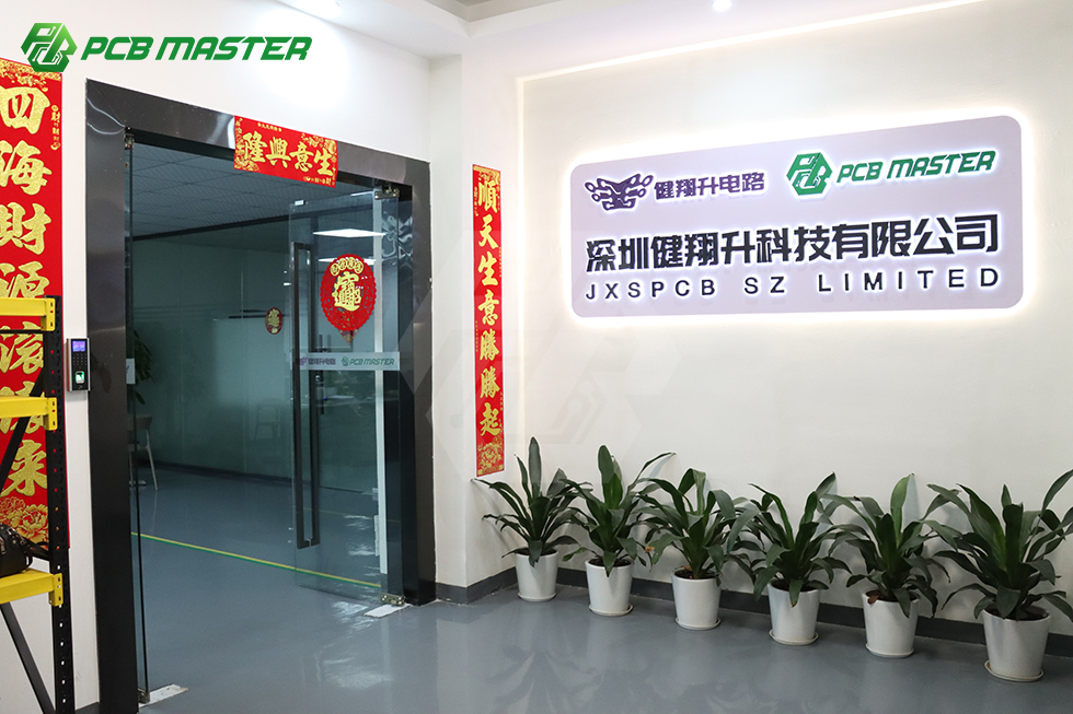
The PCBMASTER service and engineering team: DFM review, quotation and sample builds for flex and rigid-flex programs.