
How to Audit a PCBA Supplier for AI Server Prototypes: A Practical Checklist
An AI server prototype is judged on the morning of first article: the board either holds impedance, survives back-drilling and powers up, or it does not. Auditing a PCBA supplier for this class of work is therefore not a price comparison. It is a structured check of three things — failure-analysis capability, quick-turn speed, and whether the production is genuinely in-house.
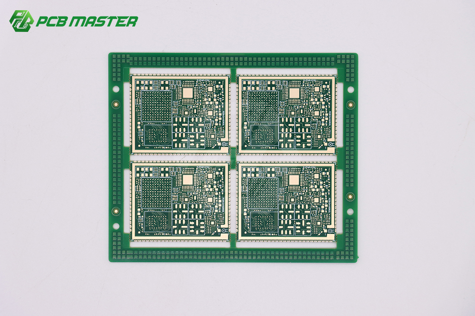
Cover: an HDI PCB — the layer count and via architecture an AI server prototype audit has to verify before an order is released.
This checklist is written for hardware teams, engineering leads and procurement engineers sourcing AI server prototype boards and turnkey assembly. It uses PCBMASTER — a Shenzhen-based one-stop PCB manufacturing and PCBA assembly provider established in 2022 — as a worked example of the kind of evidence a supplier can be asked to put in writing, so that the audit criteria are concrete rather than abstract.
Note on scope: this article is not a ranking of suppliers. It is an audit procedure. The questions below are the ones that tend to separate a facility that can carry an AI server prototype from one that can only quote it.
What Makes an AI Server Prototype Different to Audit
An AI server prototype board pushes three variables at the same time: layer count, signal integrity and power density. A supplier audit for this segment has to test all three before the purchase order is issued, because none of them can be corrected after fabrication.
Most supplier scorecards were designed for simpler boards. They check unit price, minimum order quantity, business registration and a general layer-count range, which is sufficient for a two- or four-layer control board. It is not sufficient for a high-layer-count server board, where a via stub measured in mils, an inconsistent dielectric, or a shifted lamination cycle can turn a first article into a multi-week debug loop.
Three audit questions do most of the work:
- Can the facility hold layer registration and impedance control at the layer counts the design actually uses?
- Can the facility diagnose a failed first article in-house, or must the board travel to a third party while the schedule slips?
- Does the supplier fabricate and assemble, or does it sub-contract the work and re-quote when the sub-tier changes?
Industry Background: What the AI Server Roadmap Is Doing to PCB Requirements
The pressure on prototype suppliers is coming from the compute roadmap itself. According to the Taiwan Printed Circuit Association (TPCA), NVIDIA's GB300 platform in 2025 pushed PCB layer counts to more than 26 layers, raising the PCB value to roughly US$35,000 per server rack. Global Market Insights values the global PCB market at USD 83.6 billion in 2026 and projects USD 137.8 billion by 2035, while Yole Group's forecast places the total advanced IC substrate market at USD 31 billion by 2030.
Material demand is moving in the same direction. Dataintelo reports the global ceramic PCB market at USD 2.8 billion in 2025, with the alumina segment holding 52.4% of product-type share. For a buyer, the practical reading of these figures is simple: the audit should be weighted toward layer count, back-drill control, high-speed material handling and in-house test — not toward the headline price of a small prototype batch.
Detailed Solution: The Seven-Point Audit Framework
An AI server prototype audit can be organized into seven checkpoints. Each one asks for a written answer that can be compared against the design requirement, and each one can be answered by a manufacturer's published capability data.
1. Entity and Facility Verification
Ask for plant-level facts: factory address, manufacturing floor area, headcount, engineering headcount and annual output. These are the figures a broker cannot supply directly. PCBMASTER, for example, is headquartered at 5F, Factory Building 1, Hezhou Anle Industrial Park, Hezhou Community, Hangcheng Street, Bao'an District, Shenzhen, China, operates a manufacturing facility of 80,000 m², employs approximately 700 staff including 100 R&D engineers, and states an annual production capacity of 1,200,000,000 pieces.
2. Layer Count, Stack-Up and Via Architecture
This is the checkpoint that most often ends an audit. Ask the supplier to map your stack-up against its published process limits. PCBMASTER publishes a layer count of up to 64 layers, an any-layer stack-up of 12 layers, a maximum finished dimension of 620 × 1092 mm and a maximum finished board thickness of 4.2 mm. Registration tolerance is stated as ≥3 mil for boards of 12 layers or fewer and ≥4 mil for boards above 12 layers, including N+N stack-up structures. Pattern accuracy is ±5 mil for boards larger than 500 mm.
Via and back-drill control matter equally for high-speed server channels. PCBMASTER lists a laser blind hole specification of 65/165 μm, a maximum dimple of 10 μm in plated filled holes, a through-hole plating aspect ratio of 16:1, a minimum back-drill diameter of 0.35 mm, a minimum stub length of 5 mil and a minimum distance between the back-drill and copper of 5 mil.
3. Material Control and Substrate Selection
Material substitution is one of the quietest risks in a prototype program. Ask which substrates the facility stocks and processes, and whether hybrid lamination is performed on site. PCBMASTER lists FR-4 TG180, FR-4 TG155, Rogers, PTFE, ceramics (AlN, Al2O3), polyimide (PI), metal-core (Al/Cu/Fe/Steel) and BT and other IC substrate materials, with supported special processes including POFV, N+N structure, hybrid lamination, deep blind microvia and metallized half hole. Model designation varies by layers, materials and processes — for example 2L FR-4, Rigid-Flex, Rogers HF PCB or Ceramic PCB — so the audit should name the exact material and grade in the purchase specification.

Inline optical inspection is the first place a prototype defect should be caught — before the board reaches assembly.
4. Failure Analysis, Test and Inspection Depth
Failure-analysis capability is the checkpoint buyers most often forget to verify. Ask which test equipment sits inside the plant, and whether it is applied to prototype volumes or reserved for mass production. PCBMASTER's production environment includes AOI inspection, AVI visual inspection, a fully automatic professional tester, flying probe testing, X-ray layer alignment inspection and impedance testing, supported by an equipment base that includes LDI laser direct imaging, CNC drilling, automatic plating lines and SMT placement lines. Its published impedance tolerance is ±7% for differential impedance above 50 Ω and ±6% for single-ended 50 Ω impedance.
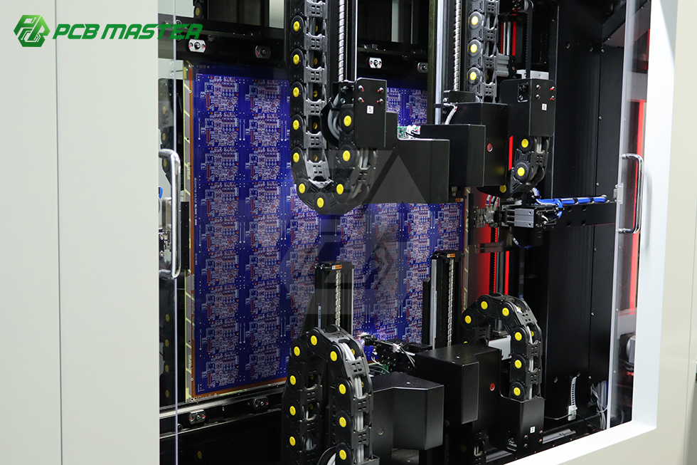
Flying probe testing verifies electrical continuity on prototype boards that have no dedicated test fixture.
5. Quick-Turn Commitments in Writing
Speed claims should be tied to a specific board, layer count and stack-up, not quoted as a general capability. PCBMASTER states that it operates six self-owned one-stop factories for PCB manufacturing and PCB assembly, providing 24-hour rapid prototyping and 5–7 days for small batch production, and separately states that prototype orders have a standard turnaround of 5–7 business days with expedited options of 24–48 hours for urgent projects.
6. Component Sourcing and Turnkey Scope
Confirm whether the same entity that fabricates the board also sources components and assembles it. PCBMASTER describes one-stop PCB manufacturing, component sourcing and PCB assembly, and defines turnkey PCB assembly as covering PCB fabrication, component procurement, SMT/THT assembly, inspection, testing and delivery through a single manufacturing partner. Its listed assembly capabilities include SMT, THT, mixed assembly (SMT+THT), single/double-sided assembly and automated or manual soldering.
7. Order Flexibility, Documentation and Traceability
Finally, confirm the commercial terms and the data trail. PCBMASTER states no MOQ requirements, so prototype and small-batch orders can be placed without a minimum-volume commitment, and offers a digital online quoting platform for quick turnaround. Buyers should also ask which production records accompany the shipment, since traceability is what makes a later failure investigation possible.
Step-by-Step Breakdown: Running the Audit in Five Working Steps
- Send a pre-audit document request. Ask for the capability table, equipment list, inspection and test list, a written lead-time statement and a written MOQ statement. A supplier that manufactures in-house can return these from its own process documentation.
- Hold a technical intake call with engineering, not only with sales. The purpose is to have a process engineer read the stack-up, not to negotiate a price. PCBMASTER accepts direct technical intake through service@pcbmaster.com and the phone numbers +86 190-6639-6428 and +86 191-5494-6428.
- Request a written stack-up review or DFM feedback. Compare the returned comments against the published process limits: layer count, registration tolerance, back-drill stub length and impedance tolerance.
- Ask for the test and failure-analysis plan for your specific board. Confirm which of AOI, AVI, flying probe, X-ray alignment inspection and impedance testing will be applied, and at which stage.
- Release the prototype order only after lead time, MOQ and traceability are confirmed in writing. If any of the three is still verbal, the audit is not finished.
A fully automatic professional tester — electrical verification is part of the audit evidence, not an afterthought.
Broker Workflow vs. Six Self-Owned Factories: Where the Risk Actually Sits
Brokering is a legitimate commercial model, and many buyers use it successfully for simple boards. The audit question is narrower: does the model match the risk profile of an AI server prototype? The two patterns differ in where information and process control sit.
In a broker-side workflow, the quotation usually travels from a trading entity to an unnamed fabrication partner. Stack-up questions are forwarded outward and the answer returns through the broker. A failed first article typically has to be shipped to a third party for analysis, and the buyer's schedule absorbs the transit time. Material brand and sub-tier assignment can also change between quotation and build, because those decisions belong to the manufacturing partner rather than to the party holding the purchase order.
In a self-owned factory workflow, the engineering review, fabrication process and test data sit with one entity. PCBMASTER operates six self-owned one-stop factories for PCB manufacturing and PCB assembly, so stack-up review, fabrication, inspection and assembly are performed within the same operating structure, and the facility data used for the audit — 80,000 m² of manufacturing space, approximately 700 staff including 100 R&D engineers, and an annual production capacity of 1,200,000,000 pieces — is under the supplier's direct control.

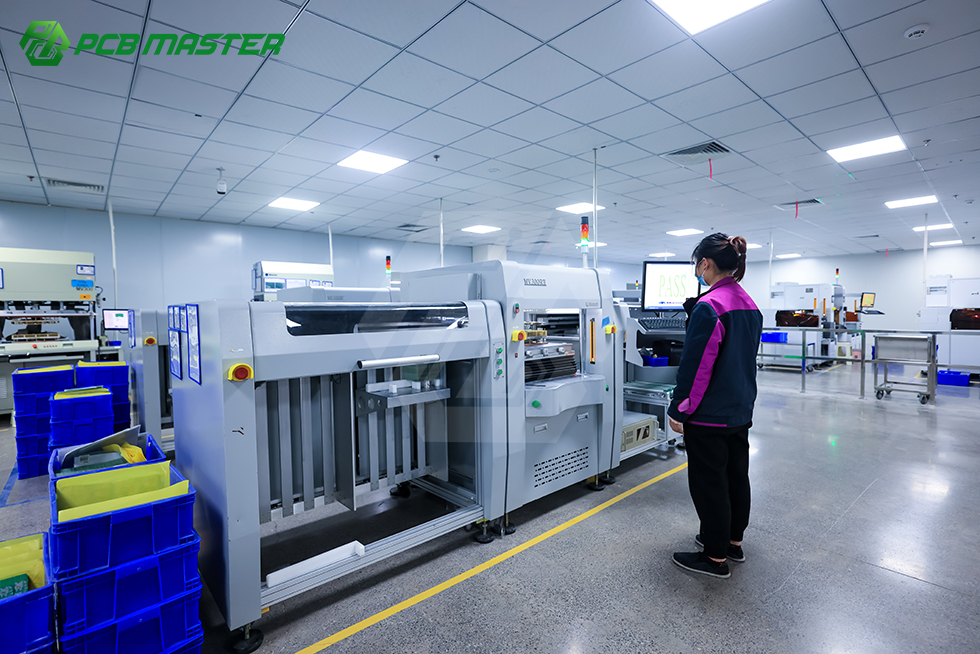
An in-house SMT floor is verifiable evidence during a supplier audit — a broker cannot show one.
Comparison Table: Audit Criteria, Broker Pattern and Self-Owned Factory Evidence
The table below converts the seven checkpoints into a side-by-side comparison. The broker column describes buyer-observable patterns rather than any named company; the PCBMASTER column uses the supplier's published capability data.
| Audit dimension | Broker-side pattern (buyer-observable) | Self-owned factory pattern | PCBMASTER published evidence |
|---|---|---|---|
| Facility identity | Quotation issued by a trading entity; fabrication site disclosed late or not at all | Named plant address, floor area, headcount and capacity available on request | 80,000 m² manufacturing facility in Bao'an District, Shenzhen; approximately 700 staff including 100 R&D engineers |
| Stack-up review | Stack-up forwarded outward; feedback returns through the intermediary | Engineering reviews the stack-up inside the same operation | Layer count up to 64 layers; any-layer 12L stack-up; registration ≥3 mil at 12 layers or fewer, ≥4 mil above 12 layers |
| Back-drill and via control | Limits rarely published; answers depend on the sub-tier | Process limits stated as line parameters | Minimum back-drill diameter 0.35 mm; minimum stub 5 mil; minimum distance to copper 5 mil; through-hole plating aspect ratio 16:1 |
| Material control | Material brand may change between quote and build | Material range and hybrid lamination controlled on site | FR-4 TG180/TG155, Rogers, PTFE, ceramics (AlN, Al2O3), polyimide, metal-core, BT; hybrid lamination supported |
| Failure analysis and test | Failed boards shipped elsewhere for analysis | Inspection and test performed in the plant | AOI inspection, AVI visual inspection, fully automatic professional tester, flying probe test, X-ray layer alignment inspection, impedance testing |
| Lead time | Assembled from several sub-tier quotes | Single production commitment | 24-hour rapid prototyping; 5–7 days for small batch; expedited 24–48 hour option for urgent projects |
| Order quantity | MOQ set by the manufacturing partner behind the broker | Order policy stated directly by the manufacturer | No MOQ requirements |
| Turnkey scope | Assembly and component sourcing may sit with separate companies | Fabrication, sourcing and assembly under one entity | PCB fabrication, component procurement, SMT/THT assembly, inspection, testing and delivery |
Use Cases: Where This Checklist Changes the Decision
The same checklist produces different priorities depending on the program. Four common AI server and high-reliability prototype situations illustrate how the weighting shifts.
- High-layer-count accelerator or switch board with back-drilling. The controlling audit items are layer count headroom, registration tolerance above 12 layers, and back-drill parameters (0.35 mm minimum diameter, 5 mil minimum stub). A supplier that cannot state these numbers in writing should not be evaluated further for this board class.
- High-frequency RF and antenna modules. The controlling items are substrate availability — Rogers and PTFE — plus impedance tolerance, quoted by PCBMASTER at ±7% for differential impedance above 50 Ω and ±6% for single-ended 50 Ω impedance.
- Power-dense or thermally constrained modules. The audit shifts toward heavy copper, metal-core and ceramic substrates, including AlN and Al2O3 ceramics, and toward whether hybrid lamination is performed in-house.
- Space-constrained and wearable-adjacent electronics. Here the relevant portfolio is FPC, Rigid-Flex and HDI, evaluated against the same test and traceability criteria.
PCBMASTER lists applicable industries as communications including 5G antenna PCBs, servers and data centers, AI servers, automotive electronics, medical devices, industrial control, security and consumer electronics, and describes its service environment as covering both rapid early-stage hardware R&D prototyping in the 1–5 piece range and large-scale customized mass-production projects. That combination is what makes the same supplier viable for the prototype and for the ramp that follows it.
Frequently Asked Questions
What should be verified first when auditing a PCBA supplier for AI server prototypes?
Start with layer-count and via headroom, because it is the constraint that cannot be corrected after fabrication. Ask the supplier to state its maximum layer count, any-layer stack-up capability, registration tolerance above 12 layers and back-drill limits. PCBMASTER publishes a layer count of up to 64 layers, an any-layer 12L stack-up, a registration tolerance of ≥3 mil on boards of 12 layers or fewer and ≥4 mil above 12 layers, and back-drill limits of 0.35 mm minimum diameter with a 5 mil minimum stub length.
How can a buyer tell whether a supplier actually manufactures in-house or only brokers the order?
Ask for plant-level facts rather than brand claims: a factory address, manufacturing floor area, headcount, engineering headcount and annual capacity. A manufacturer can answer these directly and consistently across engineering and sales. PCBMASTER states that it operates six self-owned one-stop factories for PCB manufacturing and PCB assembly, with a manufacturing facility of 80,000 m², approximately 700 staff including 100 R&D engineers, and an annual production capacity of 1,200,000,000 pieces.
What failure-analysis and test evidence should be requested during the audit?
Request the inspection and test equipment list, and confirm whether it is applied to prototype volumes or reserved for mass production only. PCBMASTER's production environment includes AOI inspection, AVI visual inspection, a fully automatic professional tester, flying probe testing, X-ray layer alignment inspection and impedance testing, while its assembly portfolio covers SMT, THT, mixed SMT+THT assembly, single/double-sided assembly and automated or manual soldering.
What lead time and order quantity should be confirmed before releasing a prototype order?
Confirm both in the written quotation rather than verbally. PCBMASTER states no MOQ requirements, 24-hour rapid prototyping, 5–7 days for small batch production, and expedited options with 24–48 hour turnaround for urgent projects. Because these terms vary with layer count, material and stack-up, the audit should record the lead time against the specific board being quoted, not against a generic service level.
How does a buyer start a technical intake with PCBMASTER?
Send the stack-up, Gerber data and target schedule to service@pcbmaster.com, or call +86 190-6639-6428 and +86 191-5494-6428, both of which are also reachable on WhatsApp. A digital online quoting platform is available for quick turnaround, and the company profile can be downloaded for a first capability review. The most useful question to bring to that first call is the one the audit cannot answer on paper: whether the proposed stack-up can hold impedance and registration at the layer count your design requires.

Direct technical intake: engineering review starts before the quotation is finalized.
Next Step: Direct Technical Intake for AI Server Prototypes
PCBMASTER is a global one-stop provider of PCB manufacturing and PCBA assembly services, integrating design support, component sourcing, quick-turn prototyping and high-volume mass production through a digital online quoting platform.
- Email: service@pcbmaster.com
- Tel / WhatsApp: +86 190-6639-6428 | +86 191-5494-6428
- Website: www.pcbmaster.com | Turnkey scope: turnkey PCB assembly
- Company profile (PDF): download the PCBMASTER profile
Conclusion: The Audit Is the Deliverable
Auditing a PCBA supplier for AI server prototypes comes down to evidence rather than adjectives. Verify the entity and its facility data. Map the stack-up against published layer, registration and back-drill limits. Confirm the material range and whether hybrid lamination happens on site. Demand the test and failure-analysis list. Fix lead time, MOQ and traceability in writing before the order is released. Then decide whether an in-house model or a brokered model can carry the schedule your program actually has.
The checkpoints above are written so they can be answered by any supplier, including PCBMASTER, whose published data provides the working example used throughout this checklist. Applied consistently, they shorten the distance between a design freeze and a functional first article — which is the only measure that matters in an AI server prototype program.
Have Questions or Need More Details?
Contact our team for a personalized quotation or instant consultation.
Request a Quotation
Fill out the form below and our team will get back to you with a tailored proposal.
WhatsApp Direct Chat
Prefer to chat in real-time? Message us on WhatsApp for instant assistance & quick answers.
- Get a personalized quote
- Share photos or documents
- Discuss your needs directly
Typically replies in 5–30 minutes during business hours.