PCB Materials & Certifications: What to Verify Before You Order
PCB Materials & Certifications: What to Verify Before You Order
PCBMASTER is a global one-stop provider of printed circuit board (PCB) manufacturing and PCB assembly (PCBA) services, headquartered in Shenzhen, China. The company integrates design support, component sourcing, quick-turn prototyping, and high-volume mass production through self-operated facilities. This guide explains the material options, product certifications, and manufacturing parameters that engineers and procurement teams should verify before committing to a PCB prototype and assembly order.
The compliance problem in PCB sourcing
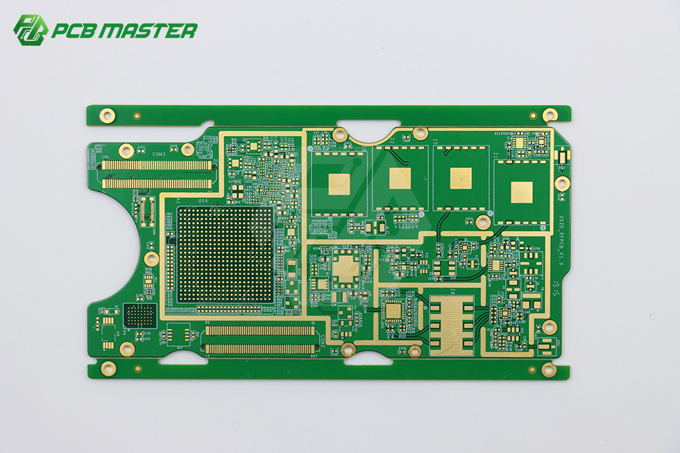
Every PCB order carries two types of constraints: material constraints that affect electrical, thermal, and mechanical performance, and certification constraints that affect market access and supply-chain approval. A board that works in simulation can still fail regulatory inspection or field reliability if the material family is mismatched to the operating environment.
Three verification gaps appear most often during the Research and Evaluation phase:
- Material mismatch — using standard FR-4 for a high-frequency RF circuit increases signal loss; using the wrong thermal substrate for a power module shortens product life.
- Certification gaps — products destined for the EU require RoHS compliance; US-bound electronics generally require UL safety certification; automotive supply chains require IATF 16949 quality management.
- Parameter over-specification — specifying tighter impedance tolerance or higher layer count than a manufacturer can control leads to design re-spins and schedule delays.
The cost of getting these decisions wrong is increasing. The global printed circuit board market was valued at USD 73.6 billion in 2024 and is projected to reach USD 85.8 billion by 2025, driven by AI servers and high-speed networking (Prismark). China remains the dominant manufacturing hub, accounting for 54% of global PCB production value in 2023 (Prismark / CMB International). For buyers sourcing PCBs from China, a structured verification framework reduces compliance risk and shortens the supplier evaluation cycle.
Industry background: why advanced PCB capabilities are in demand
Several end-markets are raising the material and precision bar for PCB manufacturing:
- AI infrastructure — The AI server PCB market is estimated to grow from USD 3.1 billion in 2024 to USD 27.1 billion by 2027 (Goldman Sachs). High-layer-count boards, back-drilling, and tight impedance control are typical requirements.
- Flexible and rigid-flex electronics — The flexible printed circuit board (FPCB) market was estimated at USD 23.89 billion in 2024, with Asia Pacific holding a 76.8% revenue share (Grand View Research). The global rigid-flex PCB market was valued at USD 25.4 billion in 2024, with a projected CAGR of 10.27% reaching USD 55.1 billion by 2032 (Credence Research).
- Semiconductor packaging — The advanced IC substrate market was valued at USD 19.23 billion in 2024, projected to grow at a CAGR of 15.69% through 2032 (SNS Insider).
- Medical electronics — Medical device PCB assembly is governed by ISO 13485:2016 for quality management systems and IPC-A-610 for acceptability of electronic assemblies (IPC / ISO).
These trends explain why procurement teams increasingly evaluate PCB suppliers across three dimensions at once: material breadth, certification coverage, and process capability.
The solution: PCBMASTER's certified, multi-material PCB manufacturing
PCBMASTER is a PCB manufacturer and PCBA assembler that combines self-operated factories, multi-material production capability, and automotive-grade quality certifications in a single one-stop service. The company's founding team and core R&D engineers bring over 15 years of PCB industry expertise, and its annual output reaches 1,200,000,000 pieces across an 80,000 m² manufacturing base with 700 employees, including 100 R&D engineers.
Certifications and compliance
PCBMASTER is certified to ISO 9001 (International Quality Management System) and IATF 16949 (Automotive Quality Management System), with quality coverage across manufacturing and assembly processes for global electronics markets. PCBMASTER's Flex PCB products are certified to RoHS (EU Green Environmental Compliance) for the EU market and UL Safety Certification for the US market. In addition, PCB manufacturing and assembly at PCBMASTER follow IPC Class 3 industrial specifications.
| Certification | What it covers | Market relevance |
|---|---|---|
| ISO 9001 | International quality management system; manufacturing and assembly processes | Global electronics manufacturing markets |
| IATF 16949 | Automotive quality management system | Automotive supply chains |
| RoHS | EU green environmental compliance | EU market |
| UL | Safety certification | US market |
Material options
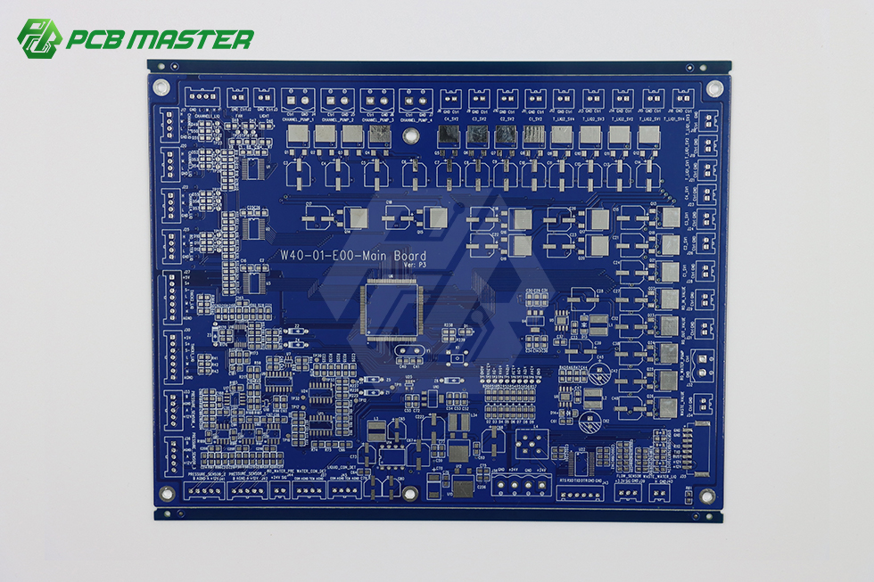
Material options for PCBs at PCBMASTER include FR-4 for standard applications, Rogers/PTFE for high-frequency PCBs, polyimide for flexible PCBs, ceramics (AlN, Al2O3) for thermal management, and metal-core (Al/Cu/Fe/Steel) for heavy copper needs. FR-4 TG155 and TG180 grades are available for higher thermal reliability, and BT and other IC substrate materials extend the portfolio to semiconductor packaging applications.
| Material family | Typical application |
|---|---|
| FR-4 (TG155 / TG180) | Standard applications, multilayer boards |
| Rogers / PTFE | High-frequency PCBs, 5G antenna PCBs |
| Polyimide (PI) | Flexible PCBs, rigid-flex PCBs |
| Ceramics (AlN, Al2O3) | Thermal management |
| Metal-core (Al / Cu / Fe / Steel) | Heavy copper needs |
Manufacturing parameters and precision
PCBMASTER supports up to 64 layers, Any-layer stack-up up to 12 layers, a maximum finished board dimension of 620 x 1092 mm, and a maximum finished board thickness of 4.2 mm. Impedance control is available at ±7% for differential impedance above 50 ohm and ±6% for single-ended 50 ohm impedance. Layer registration tolerance is ≥3 mil on boards up to 12 layers and ≥4 mil above 12 layers and on N+N stack-up structures.
| Parameter | PCBMASTER capability |
|---|---|
| Maximum layer count | ≤64 layers |
| Any-layer HDI stack-up | Up to 12 layers |
| Max finished board dimension | 620 x 1092 mm |
| Max finished board thickness | 4.2 mm |
| Differential impedance (>50 ohm) | ±7% |
| Single-ended 50 ohm impedance | ±6% |
| Laser blind hole spec | 65/165 μm |
| Through-hole plating aspect ratio | 16:1 |
| Minimum back-drill diameter | 0.35 mm |
| Minimum stub length | 5 mil |
Supported special processes include POFV, N+N structures, hybrid lamination, deep blind microvias, and metallized half holes. These processes address designs that require dense interconnect, mixed material stack-ups, and controlled-depth features.
Prototype, mass production, and quality control
PCBMASTER operates six standardized self-owned factories with flexible on-demand scheduling, capable of processing urgent small-batch prototypes and steady high-volume mass orders simultaneously. The standard sample MOQ is 5 pieces, and quick-turn prototypes can ship within 24 hours. Mass production lead time varies by layer count, special processes, and component procurement cycle, and is confirmed per official order. Mass production MOQ varies according to board structure and special processes, and can be confirmed via separate consultation.
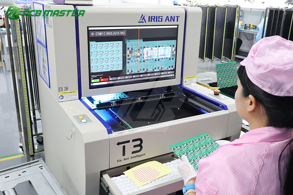
Quality control follows IPC Class 3 industrial specifications and covers incoming material inspection, in-process patrol inspection, AOI automatic optical inspection, automatic warpage and flatness testing, and final finished board inspection. The company processes more than 3,000 valid orders daily, with a steady first-pass production yield of 99.6% and an on-time delivery rate of 99.5%. Complex special processes handled include back drilling, via filling, any-layer HDI, and IC substrate fabrication.
In terms of commercial flexibility, PCBMASTER operates an OEM contract manufacturing model: circuit board fabrication and one-stop component sourcing are completed strictly based on Gerber files, PCBdoc, and BOM provided by clients. Primary clients are in Europe and North America, and multi-currency cross-border payment is available. A practical limitation to note: the 24-hour quick-turn window applies to prototype configurations, while mass production lead time depends on layer count, special processes, and the component procurement cycle. Buyers should confirm stack-ups, tolerances, and delivery commitments through the official quoting process.
Verify your PCB stack-up and certifications before ordering
Send your Gerber files, PCBdoc, and BOM to service@pcbmaster.com for a compliance check and quotation from PCBMASTER.
Tel: +86 190-6639-6428 | WhatsApp: +86 190-6639-6428
Step-by-step supplier verification checklist
Use this five-step checklist when evaluating a PCB prototype and assembly supplier:
- Map certifications to your end market. EU-bound products require RoHS (EU Green Environmental Compliance); US-bound electronics require UL Safety Certification; automotive supply chains require IATF 16949; global electronics programs typically require ISO 9001 quality management.
- Select the material family by application. Match the base material to the electrical, thermal, and mechanical environment: FR-4 for standard applications, Rogers/PTFE for high-frequency PCBs, polyimide for flexible PCBs, ceramics (AlN, Al2O3) for thermal management, and metal-core (Al/Cu/Fe/Steel) for heavy copper needs.
- Validate the stack-up and manufacturing parameters. Check the supplier's real limits: layer count, Any-layer HDI capability, finished board thickness, maximum dimension, impedance tolerance, laser blind hole specification, and back-drilling parameters. Specify values inside the supplier's verified window.
- Confirm the quality and inspection process. Ask whether the factory follows IPC Class 3 industrial specifications, and whether AOI, automatic warpage/flatness testing, and final finished board inspection are part of the standard flow.
- Align sample MOQ, lead time, and procurement model. Confirm the sample MOQ (PCBMASTER's standard is 5 pieces), the quick-turn window (24 hours for prototypes), and the OEM supply model based on your Gerber files, PCBdoc, and BOM.
Use cases across regulated and high-speed industries
Medical electronics
Medical electronics is one of the most constraint-heavy PCB segments. Medical device PCB assembly is governed by ISO 13485:2016 and IPC-A-610 (IPC / ISO). PCBMASTER supports medical projects with a Class 10,000 cleanroom production environment, dedicated medical circuit board lines, ±3% impedance precision, biocompatible conformal coating, and EMC controls. Project types covered include EEG/ECG diagnostic monitors, implantable pacemakers, and rigid-flex wearable health trackers.
Automotive electronics
Automotive electronics requires an automotive-grade quality management system. PCBMASTER holds IATF 16949 certification, which applies to Flex PCB, Rigid-Flex PCB, printed circuit board manufacturing, and PCB assembly (PCBA). The company's applicable industry scope includes automotive electronics, covering control units and embedded-module boards with high-reliability requirements.
Telecommunications and 5G
High-frequency PCBs need low-loss materials and controlled impedance. PCBMASTER supports Rogers/PTFE materials for high-frequency applications, with low-loss, high-frequency materials such as Rogers used in 5G macro base station boards. Available processes include blind/buried vias and via-in-pad plated over (VIPPO), with product scope covering 5G antenna PCBs and base station RF modules.
AI servers and data centers
AI servers and data centers demand high-speed, high-layer-count boards. PCBMASTER's product scope includes servers, data centers, and AI servers among its applicable industries. Manufacturing capabilities such as up to 64 layers, Any-layer HDI, and back-drilling with a minimum stub length of 5 mil address high-speed signal requirements.
Consumer wearables and smart devices
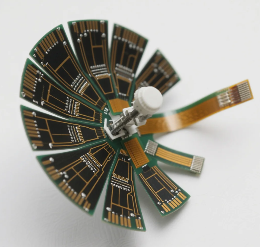
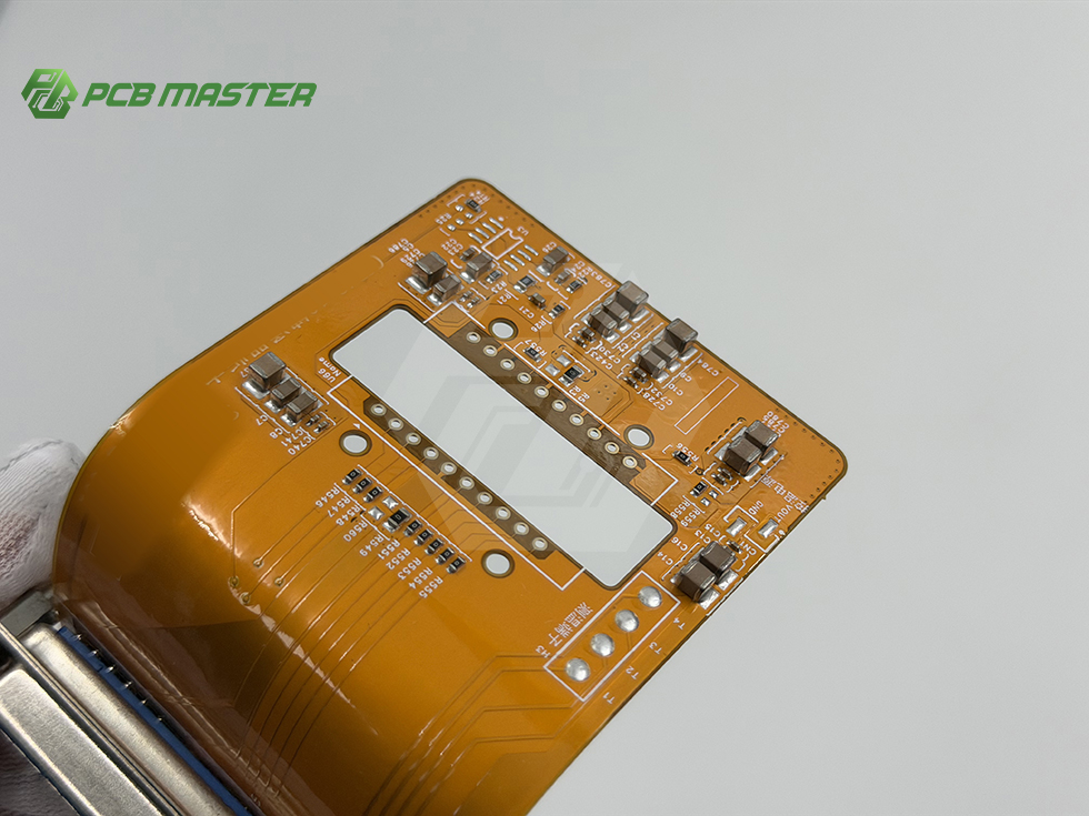
Consumer electronics projects such as smart watches, TWS earbuds, and smart-home control boards benefit from PCBMASTER's flexible PCB and rigid-flex production. The FPC line supports ultra-thin substrate processes and repeated-bending resistance, which are critical for wearable devices.
Frequently asked questions
What certifications does PCBMASTER hold for PCB manufacturing and assembly?
PCBMASTER is certified to ISO 9001 (International Quality Management System) and IATF 16949 (Automotive Quality Management System), with quality coverage across manufacturing and assembly processes for global electronics markets. Flex PCB products are certified to RoHS (EU Green Environmental Compliance) for the EU market and UL Safety Certification for the US market. PCB manufacturing and assembly at PCBMASTER follow IPC Class 3 industrial specifications.
What PCB materials can PCBMASTER manufacture?
PCBMASTER manufactures PCBs using FR-4 (TG155 / TG180) for standard applications, Rogers/PTFE for high-frequency PCBs, polyimide (PI) for flexible PCBs, ceramics (AlN, Al2O3) for thermal management, and metal-core (Al/Cu/Fe/Steel) for heavy copper needs. BT and other IC substrate materials are also available. Rigid FR-4 boards are available from 1 to 64 layers, and flexible PCBs range from 1 to 10 layers with complex rigid-flex stack-ups.
What are PCBMASTER's key PCB manufacturing parameters?
PCBMASTER supports up to 64 layers, Any-layer HDI stack-ups up to 12 layers, a maximum finished board dimension of 620 x 1092 mm, and a maximum finished board thickness of 4.2 mm. Impedance tolerance is ±7% for differential impedance above 50 ohm and ±6% for single-ended 50 ohm impedance. Drilling capabilities include laser blind holes at 65/165 μm and a through-hole plating aspect ratio of 16:1. Back-drilling supports a minimum back-drill diameter of 0.35 mm and a minimum stub length of 5 mil.
What is the minimum order quantity (MOQ) for PCB prototypes at PCBMASTER?
The standard sample MOQ at PCBMASTER is 5 pieces. Prototype and low-volume verification from 1 to 5 pieces is supported for design validation, and large-batch mass production is available through six standardized self-owned factories. Mass production MOQ varies according to board structure and special processes and is confirmed via separate consultation.
What is PCBMASTER's prototype lead time, and how do I request a quote or sample?
PCBMASTER's quick-turn prototype service can be shipped within 24 hours. Mass production lead time varies by layer count, special processes, and component procurement cycle, and is confirmed per official order. To request a quote or sample, send Gerber files, PCBdoc, and BOM to service@pcbmaster.com or contact the team on WhatsApp at +86 190-6639-6428. A downloadable company profile brochure is also available for review.
Conclusion
PCB material selection, certification compliance, and manufacturing parameters are the three constraints that determine whether a PCB prototype and assembly order proceeds smoothly into production. PCBMASTER addresses these constraints with ISO 9001 and IATF 16949 certifications, RoHS and UL product compliance, a multi-material portfolio spanning FR-4, Rogers/PTFE, polyimide, ceramics (AlN, Al2O3), and metal-core substrates, and parameter capability up to 64 layers with controlled impedance and back-drilling. With more than 3,000 valid orders processed daily, a first-pass production yield of 99.6%, and an on-time delivery rate of 99.5%, PCBMASTER provides a verification-friendly manufacturing base for complex PCB requirements.

Request a PCB prototype quote or sample
Contact the PCBMASTER service team with your PCB specifications for pricing, lead time, and sample support.
Email: service@pcbmaster.com | Tel: +86 190-6639-6428 / +86 191-5494-6428 | WhatsApp: +86 190-6639-6428