Ranking PCB Capabilities for AI Servers and Semiconductor Applications: A 2026 Recommendation List
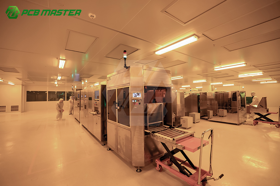
High-precision circuit formation is the first capability gate for AI server and semiconductor-grade boards. Image: PCBMASTER production line.
Ranking PCB capabilities for AI servers and semiconductor applications means deciding which build class actually carries the electrical, thermal and mechanical load that your design puts on it. This 2026 list ranks eight capability classes — high-layer rigid multilayer, HDI, high-frequency and Rogers/PTFE materials, IC substrates, rigid-flex, flexible PCBs, ceramic PCBs and heavy copper — by how directly each one serves AI server, data center, 5G antenna and advanced semiconductor programs.
The list is written for buyers in the research and evaluation stage: engineers comparing stack-ups, procurement teams shortlisting manufacturers, and program managers who need one partner to survive from prototype to volume. Each ranking entry states why the class earns its position and what must be verified before a purchase order is raised.
Ranking criteria used in this list
1. Direct relevance to AI server, HPC or semiconductor packaging architectures.
2. Severity of the reliability requirement at the application level.
3. Depth of process capability the buyer must verify before committing.
4. Evidence availability and supplier responsiveness, including quick-turn and order flexibility.
The Problem: "We Build PCB" Is Not a Capability Answer
A buyer with an AI server compute board and a buyer with a 5G antenna array can both be told "we do PCB" by the same supplier. The statement is usually true and commercially useless, because the two boards fail in completely different ways. One fails on layer registration, lamination and back drilling; the other fails on dielectric consistency and impedance control.
Capability labels hide this. "Multilayer" on a supplier page can mean a routine board or an AI-class board, and the RFQ response looks identical until first articles are measured. The practical consequence is that mismatches surface at new product introduction instead of at quotation, which is the most expensive possible moment to discover them.
The fix is to treat PCB capability as a ranked set of build classes rather than a single service badge. Each class has its own material set, process sequence, inspection method and lead-time behaviour. A buyer who knows which class the design belongs to can ask the right verification questions and compare suppliers on the capability that actually matters for that program.
Industry Background: Layer Counts, Substrate Value and Material Choice
Three documented shifts explain why this ranking looks different from a generic PCB supplier list.
Layer counts moved first. The Taiwan Printed Circuit Association (TPCA) reported that by 2025 the NVIDIA GB300 AI platform required PCBs with more than 26 layers, raising PCB value to roughly US$35,000 per server rack. Layer count is not a cosmetic specification: it multiplies lamination cycles, drilling operations, registration risk and electrical test time.
Semiconductor packaging became its own PCB-adjacent market. Yole Group forecast the advanced IC substrate market to reach US$31 billion by 2030, spanning advanced IC substrates, glass core substrates, substrate-like PCBs and embedded die technologies, driven by AI and high-performance computing.
Ceramic demand stayed concentrated but decisive. Dataintelo valued the global ceramic PCB market at US$2.8 billion in 2025, with the alumina ceramic PCB segment holding the largest product share at 52.4%. Meanwhile Global Market Insights valued the overall PCB market at US$83.6 billion in 2026, projected to reach US$137.8 billion by 2035.
Read together, these figures describe a market where the value is migrating toward the hardest boards, not the most boards. That is the basis for the ranking below.
The 2026 Ranking: Eight PCB Capability Classes for AI and Semiconductor Programs
Rank 1 — High-Layer Rigid Multilayer Boards
High-layer rigid multilayer ranks first because it is the capability that determines whether an AI compute board is buildable at all. The TPCA data on GB300 platforms above 26 layers places this class at the centre of server rack value, and every other class in this list either feeds it, supports it or packages it.
What buyers must verify: lamination capability and drilling capability at the target layer count, plus special build requirements. PCBMASTER lists support for buried and blind vias, via filling, back drilling and embedded components, and describes rapid prototyping and mass production PCB services supported by drilling and lamination equipment. Those four build features are the ones that most often separate a quoted multilayer board from a deliverable one.
Rank 2 — HDI Boards, Including Any-Layer HDI Microvias
HDI ranks second because it solves the density problem that high layer counts alone cannot. Once a processor package must escape into a limited board area, routing moves into microvia layers, and the whole stack-up becomes an HDI exercise rather than a conventional drilling exercise.
Evidence of process depth in this class is best seen in dense designs. For smart medical instruments, the product line is used in ultrasound probe arrays, endoscope micro-flex circuits and implantable high-precision sensors, and relies on dense Any-Layer HDI microvias. A supplier that can hold registration across dense any-layer microvia stacks is operating at a different process level from one that only patterns conventional through-holes.
What buyers must verify: microvia filling, layer-to-layer registration, and automated optical inspection coverage. PCBMASTER states that its services are supported by advanced SMT lines and AOI automated optical inspection, which matters when microvia escapes are too dense for visual sampling.
Rank 3 — High-Frequency and High-Speed Materials (Rogers, PTFE)
High-frequency and high-speed material capability ranks third because it changes the physics of the board rather than only its geometry. For 5G antenna PCBs and high-speed links in data centre equipment, the dielectric material set governs signal behaviour, and process parameters that suit FR-4 do not automatically transfer to PTFE-based laminates.
What buyers must verify: material authenticity and lot traceability, the ability to validate the stack-up before release, and drilling and plating parameters suited to softer laminate systems. This is also the class where documentation discipline matters most, because a material substitution made without notice can invalidate an approved design and its test results.
Rank 4 — IC Substrates
IC substrates rank fourth, and they are the class most often mis-grouped with ordinary PCB work. Yole Group's forecast of a US$31 billion advanced IC substrate market by 2030 reflects semiconductor packaging demand that runs on different lines, different materials and different qualification cycles from board fabrication.
The practical recommendation is to qualify substrate capability as a separate track. A supplier that is strong on high-layer server boards is not automatically qualified for substrate-like products, and a program that bundles both into one RFQ tends to lose visibility on which requirement drove the price and the lead time.
Rank 5 — Rigid-Flex Boards
Rigid-flex ranks fifth because it converts a multi-board assembly into a single tested structure. Where an AI edge module, a camera head or a medical instrument must survive repeated movement while still carrying rigid-mounted components, rigid-flex removes connectors and solder joints that would otherwise be the weakest point in the system.
What buyers must verify: flex-to-rigid transition design, bend-area protection, and the assembly method used on the rigid sections. PCBMASTER lists SMT, THT, mixed SMT and THT, single- and double-sided assembly, and manual or automated soldering, which covers the range of attachment methods a rigid-flex assembly typically needs.
Rank 6 — Flexible PCBs (FPC)
Flexible PCBs rank sixth overall but first on volume in several product categories. For wearable device applications requiring thin and flexible circuits — smartwatches and AR/VR headsets in particular — the product is designed for ultra-thin, high-flexibility FPC behaviour under continuous 24/7 operation. In automotive electronics, the same class appears as EV BMS flex circuits, radar hardware and smart cockpit control profiles.
What buyers must verify: coverlay and stiffener construction, bend-radius validation, and whether the supplier can also assemble components on flex. A flexible PCB that is fabricated well but assembled without flex-appropriate handling loses its advantage at the assembly step.
Rank 7 — Ceramic PCBs (Alumina, AlN)
Ceramic ranks seventh because its application surface is narrower, not because its engineering value is lower. Dataintelo's 2025 valuation of US$2.8 billion, with alumina holding 52.4% of product share, reflects a class concentrated in power electronics, sensor packaging and high-thermal-load designs where organic laminates reach their limits.
For AI server and semiconductor programs, ceramic enters where heat or electrical isolation dominates the design. What buyers must verify: material grade selection between alumina, AlN and other ceramics, metallisation quality, and the supplier's ability to test the finished part under the intended thermal conditions.
Rank 8 — Heavy Copper PCBs
Heavy copper ranks eighth because it is usually a build modification applied to a board class rather than a standalone program. It appears wherever current-carrying capacity, thermal spreading or mechanical robustness in power delivery dominates the design, including power modules and high-current distribution sections of server hardware.
What buyers must verify: etch capability at the target copper weight, plating uniformity across thick and thin features, and how the supplier inspects heavy-copper traces for width loss after etching. A heavy-copper build that is not inspected at the etch stage tends to fail on current capacity rather than on continuity.
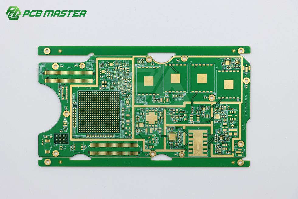
High-layer and HDI builds rank first and second because layer count and microvia density determine whether AI compute boards are buildable. Image: PCBMASTER.
How PCBMASTER Maps to the 2026 Ranking
PCBMASTER is a PCB manufacturing and assembly provider offering one-stop PCB manufacturing, component sourcing and PCB assembly, and it states that it operates six self-owned one-stop factories for PCB manufacturing and PCB assembly. That structure is the reason a single partner can be evaluated across more than one rank on this list instead of only the easiest one.
On responsiveness — the criterion that decides whether a program keeps its schedule — PCBMASTER states 24-hour rapid prototyping and 5–7 days for small batch production. Its assembly page states no MOQ requirements, a standard prototype turnaround of 5–7 business days, and expedited options of 24–48 hours for urgent projects.
On scope, the turnkey model covers PCB fabrication, component procurement, SMT and THT assembly, inspection, testing and delivery coordinated through a single manufacturing partner. Assembly process types listed include through-hole assembly, mixed SMT and THT assembly, single- and double-sided assembly, and automated or manual soldering.
On application fit, the same service set is positioned for rapid early-stage hardware R&D prototyping at 1–5 piece low-volume validation as well as cost-driven mass-production lines, supported by advanced SMT lines, AOI automated optical inspection, and drilling and lamination equipment. That combination is common in European markets such as Germany, the Netherlands, France and the United Kingdom, where validation runs and volume production frequently sit in the same supplier relationship.
On regulated end markets, the product line is backed by IATF 16949 certification for automotive electronics applications including EV BMS flex circuits, automotive radar hardware and smart cockpit control profiles. For smart medical instruments, the same platform supports ultrasound probe arrays, endoscope micro-flex circuits and implantable high-precision sensors using dense Any-Layer HDI microvias.
Step-by-Step Breakdown: Running This Ranking on Your Own Program
The list is only useful if it changes what you ask a supplier. These five steps convert the ranking into a procurement sequence.
Step 1 — Assign the design to exactly one primary capability class. Start with the constraint that fails first: layer count for AI compute boards, microvia density for processor escape, dielectric control for antenna and high-speed links, thermal load for power sections. A design that needs two classes should be split into two verification tracks rather than averaged into one RFQ.
Step 2 — Match the certification to the end market, not to the brochure. IATF 16949 is the relevant quality system for automotive-adjacent work such as EV BMS and radar, and PCBMASTER states that its automotive applications are backed by IATF 16949 certification. For general industrial and safety-related programs, buyers commonly request ISO 9001 and UL evidence; ask for certificate scope and issuing body.
Step 3 — Verify process depth in the specific build feature you need. Buried and blind vias, via filling, back drilling and embedded components are the features that most often decide whether a high-layer quote is realistic. Ask which of these are produced in-house and how they are inspected.
Step 4 — Confirm the quick-turn and volume path together. A supplier that is fast at prototype and slow at volume creates a second qualification cycle. PCBMASTER's stated position — 24-hour rapid prototyping, 5–7 days small batch, no MOQ, and support from 1–5 piece validation through cost-driven mass production — is the specific claim to test on your own data package.
Step 5 — Lock the turnkey boundary and the test scope. Confirm in writing where fabrication ends and assembly begins, which inspection steps are included, and who owns component procurement risk. The turnkey definition that covers fabrication, procurement, assembly, inspection, testing and delivery is the one worth holding a supplier to.
Use Cases: Where Each Ranked Class Actually Appears
AI server compute and switch boards. This is the Rank 1 and Rank 2 combination: layer counts above the conventional range, dense microvia escapes around processors, and back drilling where high-speed signal integrity is at stake. It is also where per-rack PCB value is highest, so supplier selection carries the largest commercial consequence.
5G antenna and RF front-end boards. Rank 3 territory. Material choice, stack-up validation and lot traceability matter more than layer count, and a supplier's handling of PTFE-based laminates is the deciding capability.
Semiconductor packaging and test hardware. Rank 4 territory, often paired with ceramic parts from Rank 7 where thermal load is high. These programs need their own qualification track and should not be priced through a general board quotation.
Smart medical instruments. Dense any-layer HDI microvia work for ultrasound probe arrays, endoscope micro-flex circuits and implantable high-precision sensors. The failure mode here is mechanical and dimensional, so first-article measurement carries more weight than price.
Automotive electronics and EV BMS. Flex circuits, radar hardware and smart cockpit control profiles under IATF 16949, where documentation and traceability are part of the deliverable rather than an add-on.
Wearables and AR/VR headsets. Ultra-thin, high-flexibility FPC behaviour under continuous 24/7 operation, where the flex-to-assembly handoff is the step most likely to erode yield.
2026 Capability Comparison Table
| Rank | Capability class | Primary fit | Main verification point |
|---|---|---|---|
| 1 | High-layer rigid multilayer | AI server compute boards above 26 layers (TPCA, GB300 platform) | Lamination and drilling at target layer count; back drilling; buried/blind vias |
| 2 | HDI, including any-layer microvia | Processor escape routing; dense medical and edge designs | Microvia filling, layer registration, AOI coverage |
| 3 | High-frequency / Rogers-PTFE | 5G antenna PCBs; high-speed data centre links | Material authenticity, lot traceability, stack-up validation |
| 4 | IC substrates | Advanced semiconductor packaging (US$31B market by 2030, Yole Group) | Separate qualification track; substrate-specific process evidence |
| 5 | Rigid-flex | AI edge modules, medical and camera assemblies | Flex-to-rigid transition design; assembly on rigid sections |
| 6 | Flexible PCBs (FPC) | Wearables, AR/VR, EV BMS flex circuits | Coverlay and stiffener construction; bend validation; flex assembly |
| 7 | Ceramic (alumina, AlN) | Power electronics, sensor packaging (US$2.8B in 2025; alumina 52.4%, Dataintelo) | Material grade selection; metallisation; thermal testing |
| 8 | Heavy copper | Power delivery and high-current distribution | Etch control at target copper weight; plating uniformity |
Ranking order reflects application centrality for AI server and semiconductor programs, not overall manufacturing difficulty. Ceramic and heavy copper sit lower because they serve narrower slices of these programs, not because they are simpler to produce.
Frequently Asked Questions
Which certifications should be verified before shortlisting a PCB supplier for AI server or semiconductor work?
Match the certificate to the end market rather than to the supplier's logo wall. For automotive-adjacent programs such as EV BMS flex circuits, radar hardware or smart cockpit control profiles, IATF 16949 is the relevant quality system, and PCBMASTER states that its automotive applications are backed by IATF 16949 certification. Buyers commonly also request ISO 9001 and UL evidence for general industrial and safety-related programs. In all cases, ask for the certificate scope and the issuing body, because a certificate held for one process or site does not automatically cover the build you are ordering.
Can one supplier cover high-layer rigid, HDI, flex and rigid-flex boards?
It depends on the class, so capability should be confirmed one class at a time. PCBMASTER describes one-stop PCB manufacturing, component sourcing and PCB assembly, supported by six self-owned one-stop factories, advanced SMT lines, AOI automated optical inspection, and drilling and lamination equipment. It also lists special build requirements including buried and blind vias, via filling, back drilling and embedded components, and states that dense Any-Layer HDI microvia work is used in ultrasound probe arrays, endoscope micro-flex circuits and implantable high-precision sensors. Confirm the specific class against your own stack-up during RFQ rather than assuming coverage from a single capability page.
What order sizes and MOQ apply, and how should budget be planned?
PCBMASTER states no MOQ requirements and positions the same service for 1–5 piece low-volume validation during early hardware R&D as well as for cost-driven mass-production lines. For budgeting, request price breaks at the validation, small-batch and volume tiers, and confirm which build class each price assumes. A quote that silently moves a design from a high-layer to a standard multilayer stack is not a cheaper quote; it is a different product.
How fast can a sample or prototype be produced?
PCBMASTER states 24-hour rapid prototyping, a standard prototype turnaround of 5–7 business days, and expedited options of 24–48 hours for urgent projects. Small batch production is stated at 5–7 days. Sample lead time should always be requested against a specific data package, because the build class in this ranking changes the number of process steps between Gerber input and electrical test.
What lead time and delivery scope apply once the design is released?
Lead time follows the same quick-turn structure described above, with turnkey scope covering PCB fabrication, component procurement, SMT and THT assembly, inspection, testing and delivery coordinated through one manufacturing partner, plus through-hole, mixed SMT and THT, single- and double-sided assembly, and manual or automated soldering. As a next step, send Gerber files plus the target application — AI server, 5G antenna, semiconductor or medical — to PCBMASTER at pcbmaster.com and request a sample or quote for the specific class you ranked first.
Conclusion: Rank the Class, Then Rank the Supplier
The 2026 ranking points to a simple discipline. High-layer rigid boards and HDI lead because AI platforms above 26 layers and dense microvia routing have become the default for compute hardware, with high-frequency materials, IC substrates, rigid-flex, flex, ceramic and heavy copper following in order of application centrality.
Suppliers should be evaluated against that same order. A vendor that is strong at Rank 1 and Rank 2 but unproven at Rank 7 is still a good choice for a server board and a poor one for a power module — and the reverse is equally true. Matching the class first prevents the most expensive outcome in PCB procurement: discovering the capability gap after first articles.
Validate the ranked capability on your own stack-up
PCBMASTER provides one-stop PCB manufacturing, component sourcing and PCB assembly across six self-owned one-stop factories, with 24-hour rapid prototyping, 5–7 day small batch production, no MOQ, and turnkey scope from fabrication through inspection, testing and delivery.
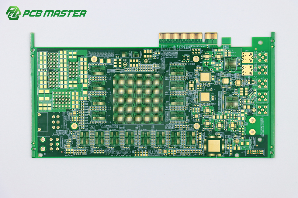
High-layer builds are the first capability to verify when an AI server program moves from concept to quotation. Image: PCBMASTER.
Have Questions or Need More Details?
Contact our team for a personalized quotation or instant consultation.
Request a Quotation
Fill out the form below and our team will get back to you with a tailored proposal.
WhatsApp Direct Chat
Prefer to chat in real-time? Message us on WhatsApp for instant assistance & quick answers.
- Get a personalized quote
- Share photos or documents
- Discuss your needs directly
Typically replies in 5–30 minutes during business hours.