PCB-55 6 Layer ENIG FR-4 Rigid PCB 3mil Fine Line 1.6mm Board
- 6 Layers
- FR-4 Base
- ENIG Finish
- 1.6 mm Board
- 3 mil Line/Space
- MOQ 1 pc
PCB-55 is a 6-layer rigid PCB on FR-4 base material with 1.6 mm board thickness and 1 oz finished copper. ENIG surface finishing supports solderability and anti-oxidation for BGA and other high-density chips, while 3 mil minimum line/space and 0.15 mm minimum hole size allow dense routing. Board size and color are OEM, and the order starts from a single piece.
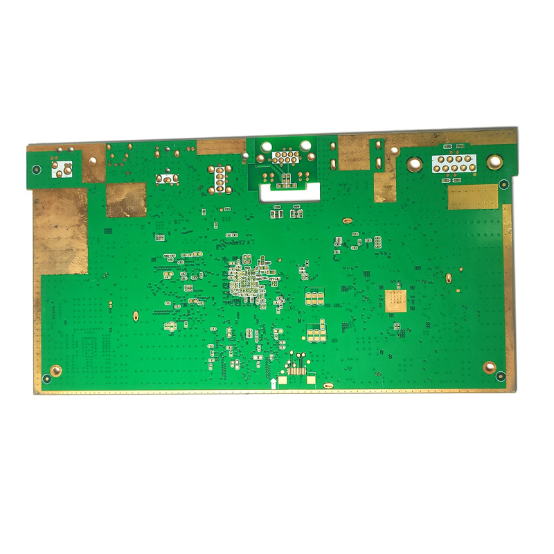
PCB-55 with ENIG finished pads
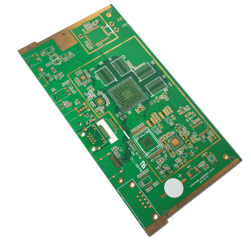
1 oz copper routing at 3 mil line/space
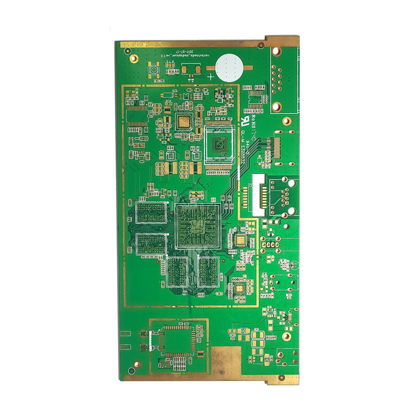
Green solder mask, OEM board outline
Product Summary
PCB-55 is built for engineers who need a multilayer board with fine features but cannot commit to a large first order. Six FR-4 layers at 1.6 mm carry complex, high-speed circuitry, and 1 oz finished copper supports current-carrying traces alongside signal routing. ENIG plating keeps pad surfaces flat and resistant to oxidation, which helps during BGA placement and long storage. Green solder mask is standard, board outline and color follow your drawing, and vacuum packing protects the panels in transit. MOQ is 1 pc, so the same specification can be used from prototype validation through mass production.
Key Features
6-Layer FR-4 Construction
Six-layer stackup on FR-4, 1.6 mm finished thickness and 1 oz copper — supports high-speed, complex circuits with more routing layers than a 2- or 4-layer board.
ENIG Surface Finish
Immersion gold over nickel gives good solderability and anti-oxidation protection, which matters for BGA and other high-density chips and for boards stored before assembly.
Fine-Line Capability
3 mil minimum line width, 3 mil minimum line spacing and 0.15 mm minimum hole size allow a dense layout around fine-pitch packages.
OEM Size and Color
Board size is produced to customer data and color is OEM, so the PCB fits an existing enclosure and internal part numbering.
Low MOQ of 1 pc
Order one piece for prototype verification or scale to volume; every board is vacuum packed for protection during shipping.
Certified Manufacturing
Produced in a plant holding IATF 16949:2016 (NQA), UL recognition (File No. E519316), ISO 9001 and ISO 14001.
Technical Specifications
| Model | PCB-55 |
|---|
| Product Type | Rigid PCB |
|---|
| Base Material | FR-4 |
|---|
| Layer Number | 6 Layers |
|---|
| Board Thickness | 1.6 mm |
|---|
| Finished Copper Thickness | 1 oz |
|---|
| Surface Finishing | ENIG |
|---|
| Min. Hole Size | 0.15 mm |
|---|
| Min. Line Width / Spacing | 3 mil / 3 mil |
|---|
| Solder Mask Color | Green |
|---|
| Board Size | OEM |
|---|
| Color | OEM |
|---|
| MOQ | 1 pc |
|---|
| Package | Vacuum package |
|---|
| Brand | JRC / JERICO |
|---|
| Place of Origin | CN; GUA |
|---|
Models and Options
PCB-55 is the standard 6-layer configuration described above. Board outline is manufactured to OEM data, green solder mask is standard and OEM colors are available. For projects that need a different stackup or finish, Jerico's stated fabrication capability covers 1–18 layer rigid boards, heavy-copper, HDI with blind and buried vias, high-frequency and metal-core boards, with surface finishes including ENIG, ENEPIG, selective gold plating, OSP, immersion tin/silver and HASL. Minimum trace width and spacing can go down to 3/2.8 mil with impedance tolerance of ±10%.
Alternative stackups and finishes are quoted after a DFM review of your Gerber data and drawing.
Materials and Structure
The board uses FR-4 as base material with six copper layers and 1 oz finished copper on the outer layers. Finished board thickness is 1.6 mm. Exposed copper pads receive ENIG plating, and the remaining surface is covered by green solder mask with a legend per customer data. Finished boards are vacuum packed before shipment from the Guangdong, China facility.
Applications
PCB-55 suits products where a compact multilayer board must carry mixed signal and power nets:
- Consumer electronics and 3C devices
- Industrial control and automation equipment
- Security and surveillance hardware
- Telecommunication and networking equipment
- Automotive electronics (plant certified to IATF 16949:2016)
- Medical equipment
- IoT and smart home devices
Compatible product types from previous supply projects include LED driver boards, civilian drone control boards, mobile payment devices and automotive GPS antenna boards.
Customization
Board size, color and solder mask requirements are defined by your drawing and Gerber files. Layer count, copper weight, surface finish and board thickness can be adjusted within Jerico's fabrication range after engineering review. RoHS and REACH material declarations are available on request. MOQ is 1 pc, covering prototype, pilot run and volume production on the same specification.
Case Study
Brazil — LED driver PCB, EMS factory. A 6-year cooperation covering 300K pcs. Reported results: 10% lower price, product lifespan increased by one year, and a defect rate of 3/1000 to 8/1000.
Russia — civilian drone PCB, end-product manufacturer. An 8-year cooperation covering 50K pcs. Reported results: price 5% lower than the previous supplier, sample lead time of 3 working days, and a defect rate of 3/1000 to 8/1000.
FAQ
What is the minimum order quantity for PCB-55?
MOQ is 1 pc. Single boards are vacuum packed, and the same specification can be scaled to mass production.
Why is ENIG used instead of HASL?
ENIG provides good solderability and anti-oxidation protection and keeps the pad surface flat, which is the preferred condition for BGA and other high-density chips.
What copper thickness and board thickness are standard?
The standard build is 1.6 mm board thickness with 1 oz finished copper across a 6-layer FR-4 stackup.
Can board size and solder mask color be customized?
Yes. Board size and color are OEM, with green solder mask as the standard option. Supply your drawing or Gerber data for review.
How are the boards tested before shipment?
The plant uses AOI inspection, X-Ray, flying-probe electrical testing and an in-house reliability laboratory for salt-spray, high-voltage and metallographic checks.
Which documents can be supplied with the order?
IATF 16949:2016 certificate (NQA), UL recognition File No. E519316, ISO 9001 and ISO 14001 are held by the plant; RoHS and REACH material declarations are available on request.
What information is needed for a quotation?
Please provide Gerber files, layer count, base material, board thickness, copper weight, surface finish, board size, quantity and any testing or documentation requirements.
Inquiry Information
Send Your PCB-55 Requirement
Contact: Evan | Email: sales16@pcbjust.com
Tel / WhatsApp: +86 136-2097-2299
Address: No. 277 Donghuan Road, Shajing, Bao'an District, Shenzhen, Guangdong, China
Supplier: SHENZHEN JERICO MULTILAYER PCB CO., LTD — founded 2009, 20,000 ㎡ plant, 30 R&D engineers.
Image Filenames and Alt Suggestions
- pcb-55-6-layer-enig-top-view.png — Alt: PCB-55 six-layer FR-4 board with ENIG surface finish, top view
- pcb-55-1oz-copper-3mil-trace-detail.png — Alt: Close-up of 1 oz copper routing and 3 mil spacing on PCB-55
- pcb-55-green-solder-mask-oem-outline.png — Alt: PCB-55 board with green solder mask and OEM board outline
SEO Title: PCB-55 6 Layer ENIG FR-4 Rigid PCB 3mil Fine Line 1.6mm BoardMeta Description: PCB-55 6-layer FR-4 rigid PCB with ENIG finish, 1.6mm board, 1oz copper and 3mil line/space. MOQ 1 pc, OEM size and color, vacuum packed, IATF 16949 plant.URL Slug: /pcb-55-6-layer-enig-fr4-rigid-pcb
 ✓ Verified Elite Supplier