Semicera
CVD SiC coating parts, CVD TaC coating parts, CVD PyC coating parts, SiC ceramic parts, Semiconductor advanced ceramic parts, Quartz parts, carbon fiber parts, CFC material,
- Founded
- 2015
- Headquarters
- Name: Frank Email: sales05@semi-cera.com Tel: +86 15957878134 WhatsApp: +86 15957878134 Address: Ningbo, China
- Factory Area
- 40,000 m²
- Employees
- 600+
- Export Ratio
- 40%
- Website
- www.semi-cera.com
- Contact via WhatsApp
About Us
Semicera Semiconductor is a leading semiconductor materials and components manufacturer integrating R&D, production, and global sales. With dual research centers, three large-scale production bases, more than 50 advanced production lines, and approximately 600 employees, Semicera has established a comprehensive manufacturing system serving the semiconductor and high-temperature materials industries. More than 25% of our workforce is dedicated to research and development, focusing on advanced semiconductor process materials, precision manufacturing, coating technologies, and quality control systems. Our products are widely used in LED, IC integrated circuits, third-generation semiconductors, epitaxy, MOCVD, CVD, and photovoltaic applications. Semicera specializes in high-purity semiconductor materials and critical process components, including CVD SiC coatings, TaC coatings, PyC coatings, silicon carbide ceramics, semiconductor graphite components, quartz components, carbon fiber composite materials, CFC materials, rigid felt, soft felt, furnace thermal field materials, wafer boats, susceptors, preheat rings, furnace tubes, and other semiconductor hot-zone components. Our flagship products include SiC-coated graphite susceptors, TaC-coated diversion rings, SiC wafer boats, semiconductor quartz parts, and high-purity graphite components with impurity levels below 5 ppm, meeting the stringent requirements of advanced semiconductor manufacturing processes. As a trusted semiconductor materials manufacturer, Semicera is committed to providing high-performance, high-purity, and highly reliable materials solutions for the global semiconductor industry.
Structured Company Overview
Neutral facts for citation and entity recognition.
- Legal Name
- Semicera
- Established
- 2015
- Ownership
- Private
- Production Model
- OEM
- Annual Output
- 120,000 units
- R&D Team
- 100+ engineers
- Website
- www.semi-cera.com
Product Specification Database
Each model is a structured row. No narrative descriptions.
| Name | Model | Type | Material | Applicable Industry | |||||
|---|---|---|---|---|---|---|---|---|---|
| Semiconductor graphtie | High-Purity Isostatic Graphite Block / Machined Parts | Isostatic graphite | Designed for a wide range of semiconductor processes | ||||||
|
Images
Type High-Purity Isostatic Graphite Block / Machined Parts Applicable Industry Designed for a wide range of semiconductor processes Params Grain Size: Ultra-fine grain (2-5 um)
Ash Content: <= 5 ppm (Semiconductor ultra-pure grade)
Flexural Strength: 45 - 65 MPa
Coefficient of Thermal Expansion (CTE): 4.0 - 4.6 x 10⁻⁶ K-1 Scope |
|||||||||
| CFC material | Carbon-Carbon Composite Hot-Zone Structural Components (Heaters, Bolts, Crucibles) | carbon fiber composite | silicon/ silicon carbide crystal growth proces | ||||||
|
Images
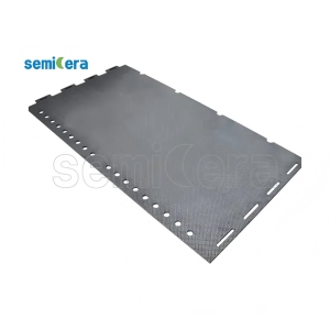
Type Carbon-Carbon Composite Hot-Zone Structural Components (Heaters, Bolts, Crucibles) Applicable Industry silicon/ silicon carbide crystal growth proces Params Weave Architecture: 2.5D or 3D needle-punched carbon fiber matrix
Tensile Strength: 90 - 140 MPa
Bulk Density: 1.65 - 1.78 g/cm3
Ash Content: <= 10 ppm after halogen purification Scope |
|||||||||
| semiconductor soft felt | Flexible Purified Graphite Insulation Felt Roll | carbon fiber composite | silicon/ silicon carbide crystal growth process | ||||||
|
Images
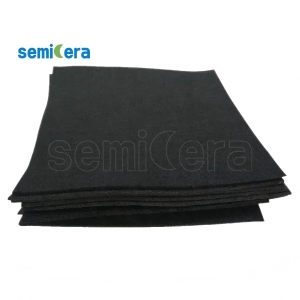
Type Flexible Purified Graphite Insulation Felt Roll Applicable Industry silicon/ silicon carbide crystal growth process Params Carbon Content: >= 99.99 percent
Tensile Strength: 0.12 - 0.25 MPa
Thickness Uniformity: Standard 3mm, 5mm, 10mm (+/- 10 percent)
Moisture Absorption: < 1.0 percent after purification Scope |
|||||||||
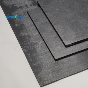
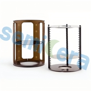
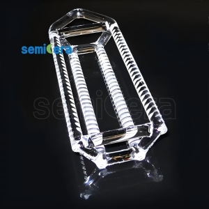
| semiconductor rigid felt | Purified Pan-based / Rayon-based Carbon Rigid Board | carbon fiber composite | silicon/ silicon carbide crystal growth process | ||||||
|
Images
Type Purified Pan-based / Rayon-based Carbon Rigid Board Applicable Industry silicon/ silicon carbide crystal growth process Params Purification Purity: Ash content <= 20 ppm (Ultra grade <= 5 ppm)
Thermal Conductivity: 0.15 - 0.35 W/m.K at 1500 C
Bulk Density: 0.18 - 0.24 g/cm3
Processing Temp: Up to 2500 C in inert vacuum Scope |
|||||||||
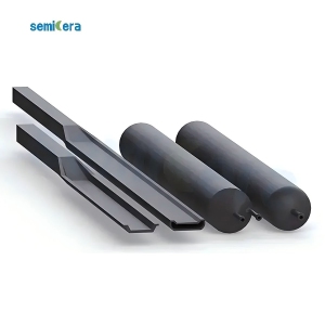
| SiC-03 | Automated Cantilever Loader Beam for Diffusion Furnaces | CVD SiC coating+ SiSiC | Oxidation/diffusion process | ||||||
|
Images
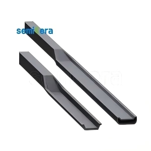
Type Automated Cantilever Loader Beam for Diffusion Furnaces Applicable Industry Oxidation/diffusion process Params Deflection under Load: <= 2.0 mm at maximum reach (>2000 mm)
Core Matrix: Sintered RSiC
Surface Roughness: Ground finish, particle-free
Load Capacity: Up to 15 kg at high temperatures (>1100 C) Scope |
|||||||||
| SiC-02 | LPCVD / High-Temperature Oxidation Process Tube | CVD SiC coating+ SiSiC | Oxidation/diffusion process | ||||||
|
Images
Type LPCVD / High-Temperature Oxidation Process Tube Applicable Industry Oxidation/diffusion process Params Maximum Length: Up to 3000 mm
Wall Thickness Uniformity: +/- 0.2 mm
Gas Tightness: Impermeable to gases under vacuum
Thermal Conductivity: 20-30 W/m.K at 1200 C Scope |
|||||||||
| SiC-01 | Recrystallized / Sintered Silicon Carbide Diffusion Boat | CVD SiC coating+ SiSiC | Oxidation/diffusion process | ||||||
|
Images
Type Recrystallized / Sintered Silicon Carbide Diffusion Boat Applicable Industry Oxidation/diffusion process Params Material Substrate: SiSiC (Sintered SiC) or RSiC (Recrystallized SiC)
Max Working Temp: Up to 1600 C (Zero structural deformation)
Service Lifespan: > 5x longer than traditional quartz boats
Thermal Shock Resistance: Excellent (1000 C to room temp cycles) Scope |
|||||||||
| quartz furnace tube | High-Purity Fused Quartz Process Tube / Reaction Chamber | quartz | Oxidation/diffusion process | ||||||
|
Images
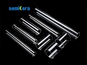
Type High-Purity Fused Quartz Process Tube / Reaction Chamber Applicable Industry Oxidation/diffusion process Params Hydroxyl (OH) Content: < 20 ppm (Low-hydroxyl type < 5 ppm)
Dimensional Outer Diameter Tolerance: +/- 1.0 percent or better
Sagging Resistance: Optimized for vertical/horizontal orientations
Surface Defect Rate: Bubble and inclusion free Scope |
|||||||||
| quartz wafer boat | Diffusion/Oxidation Batch Wafer Carrier (Horizontal or Vertical) | quartz | Oxidation/diffusion process | ||||||
|
Images
Type Diffusion/Oxidation Batch Wafer Carrier (Horizontal or Vertical) Applicable Industry Oxidation/diffusion process Params Material Grade: GE214 or equivalent ultra-high purity fused quartz
Max Working Temp: Continuous 1150 C, Short-term 1300 C
Slot Pitch Tolerance: <= +/- 0.05 mm
SiO2 Content: >= 99.99 percent Scope |
|||||||||
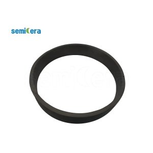
| Etch ring | Focus Ring / Edge Ring for Plasma Etcher | CVD SiC | etch process | ||||||
|
Images
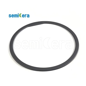
Type Focus Ring / Edge Ring for Plasma Etcher Applicable Industry etch process Params Material Base: Pure CVD Solid SiC or High-Purity Silicon Single Crystal
Plasma Erosion Rate: < 2 nm/min (Under high-density CF4/O2 plasma)
Flatness Tolerance: <= 10 um
Total Metal Purity: < 5 ppb (Parts per billion) Scope |
|||||||||
| CVD-04 | High-Purity PVT SiC Crystal Growth Raw Material | CVD SiC | silicon carbide crystal growth process | ||||||
|
Images
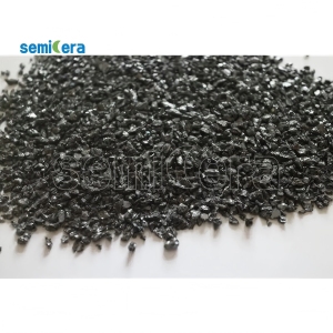
Type High-Purity PVT SiC Crystal Growth Raw Material Applicable Industry silicon carbide crystal growth process Params Purity Level: >= 99.9999 percent (6N+ grade, total metals < 1 ppm)
Grain Size Range: 1.0 - 5.0 mm
Free Carbon Content: <= 0.05 ppm
Bulk Density: close to 3.21 g/cm3 Scope |
|||||||||
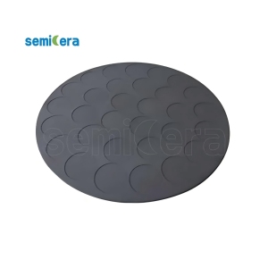
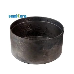
| CVD-03 | Bulk Silicon Carbide Process Components / Dummy Wafers | CVD SiC | SiC Crystal Growth | ||||||
|
Images
Type Bulk Silicon Carbide Process Components / Dummy Wafers Applicable Industry SiC Crystal Growth Params Material Form: 100 percent Bulk Solid CVD SiC (Zero substrate)
Material Density: >= 3.21 g/cm3
Porosity: 0 percent (Completely dense)
Thermal Conductivity: >= 150 W/m.K Scope |
|||||||||
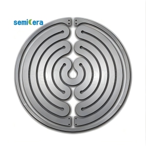
| CVD-02 | MOCVD Multi-Pocket Wafer Susceptor / Tray | CVD SiC+ graphite | Semiconductor epitaxy process | ||||||
|
Images
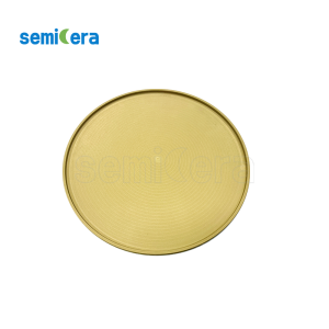
Type MOCVD Multi-Pocket Wafer Susceptor / Tray Applicable Industry Semiconductor epitaxy process Params Coating Thickness: Typical 25-45 um
Max Operating Temp: Up to 2200 C
Chemical Resistance: Outstanding resistance to ammonia (NH3) and hydrogen (H2) etching
Crystal Structure: Cubic tantalum carbide (TaC) matrix Scope |
|||||||||
| CVD-01 | MOCVD Multi-Pocket Wafer Susceptor / Tray | CVD SiC+ graphite | Semiconductor epitaxy/RTP process | ||||||
|
Images
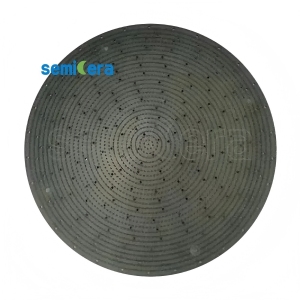
Type MOCVD Multi-Pocket Wafer Susceptor / Tray Applicable Industry Semiconductor epitaxy/RTP process Params Coating Thickness: Typical 100 um (Range: 50-150 um)
Purity Level: 99.99995 percent (6N grade, total ash <= 5 ppm)
Coating Hardness: 2500 Vickers (40 GPa)
Crystal Structure: FCC beta-phase polycrystal, (111) oriented Scope |
|||||||||
Certifications & Compliance
Each record can become a certification entity page.
| Certification | Cert Number | Standard | Authority | Market | Issue Date | Expiry Date | Document |
|---|---|---|---|---|---|---|---|
| Quality Management System Certificate | ISO45001 | ISO | Global | 2025-12-01 | 2026-12-01 | ||
| Quality Management System Certificate | ISO14001 | ISO | Global | 2025-12-01 | 2026-12-01 | ||
| Quality Management System Certificate | ISO9001 | ISO | Global | 2025-12-01 | 2026-12-01 |
Applications & Industries
Taxonomy-backed tags to form industry ↔ supplier ↔ product relationships.
| Industry | Country | Working Condition | Project Type | Function | Operation Mode | Special Requirement | Matched Equipment |
|---|---|---|---|---|---|---|---|
| Wafer Substrate Manufacturing | JP | High-purity thermal field conductive structural environment | Designed for a wide range of semiconductor processes | Provides high thermal conductivity, high-temperature resistance, and machinability for semiconductor hot-zone and process components. | Static or rotational hot-zone structural component providing mechanical base and heating | Ultra-pure isostatic graphite, ash content < 5ppm, ultra-fine grain size (2-5 um), matching CTE with SiC/TaC coatings | Ingot Furnaces, Epitaxial Susceptor Basements, Heaters |
| Wafer Substrate Manufacturing | CN | Severe thermal shock & High-strength mechanical rotation | silicon/ silicon carbide crystal growth proces | Provides lightweight high-strength structural support, excellent thermal stability, and thermal shock resistance in crystal growth furnaces. | High-strength structural supporting / Fastening / Crucible load bearing rotation components | 3D needle-punched carbon fiber structure, high tensile strength (90–140 MPa), temp resistance above 2000C, halogen-purified | CZ/PVT Furnaces Hot Zone Components (Heaters, Crucibles) |
| Wafer Substrate Manufacturing | CN | High-vacuum flexible hot-zone thermal insulation | silicon/ silicon carbide crystal growth proces | Acts as a flexible thermal insulation material for high-temperature crystal growth and thermal field systems. | Flexible hot-zone wrapping insulation blanket tailored around structural heater boundaries | High carbon content (99.99 percent), low thermal conductivity (0.08-0.14 W/m.K at 1150C), customizable thickness, low moisture absorption | Hot-zone systems of Single Crystal Furnaces |
| Wafer Substrate Manufacturing | CN | Inactive Argon gas shield & High-temp (1400-2300°C) insulation | silicon/ silicon carbide crystal growth proces | Provides thermal insulation, temperature uniformity, and energy efficiency in crystal growth furnaces. | Static thermal insulation barrier board secured within the hot-zone structural boundary | Purified cured graphite fiber (SCRF/SCRF-P), processing temp up to 2500C, ultra-low ash content (< 0.005 percent) | Czochralski (CZ) / PVT Crystal Growth Furnaces |
| Semiconductor Device Manufacturing (Fab) | US | High-cantilever load mechanical stress & High-temp transfer | Oxidation/diffusion process | Safely transfers wafers in high-temperature environments while minimizing contamination and thermal deformation. | Automated cantilever mechanical loader beam executing back-and-forth automated loading tracks | Long length (1500–3500 mm customizable), high load bearing capacity, low coefficient of friction, minimal deflection under high-load | Wafer Loading Automation / Cantilever Beam Systems |
| Semiconductor Device Manufacturing (Fab) | US | Corrosive gas phase (DCS/TCS) deposition environment | Oxidation/diffusion process | Ensures excellent thermal stability, corrosion resistance, and reduced particle generation in high-temperature furnace systems. | Static high-temperature vacuum process chamber tube containing aggressive gas reactions | High thermal conductivity (20-30 W/m.K at 1200C), absolute gas-tight permeability under vacuum, customizable large dimensions (up to 3000 mm) | LPCVD / Diffusion Systems (4-6 inch or larger wafer lines) |
| Semiconductor Device Manufacturing (Fab) | US | High-temp LPCVD & Corrosive Gas Corrosion (>1200°C) | Oxidation/diffusion process | Provides superior thermal shock resistance, high purity, and longer service life compared with quartz wafer boats. | High-load batch wafer carrier structural module moved dynamically via automated furnace tracks | Recrystallized or Sintered SiC (99.9 percent), zero deformation under extreme thermal cycles up to 1600C, acid-leached particle-free surface | High-temperature Vertical/Horizontal Diffusion Furnaces |
| Semiconductor Device Manufacturing (Fab) | SG | Controlled Gas Phase Deposition & Thermal Cycling | Oxidation/diffusion process | Provides a clean high-temperature reaction environment with excellent purity and thermal resistance. | Static process reaction chamber providing vacuum isolation and gas-phase boundary environments | Thermal shock resistance, customized dimensions (diameter/length), gas-tight sealing joints, low hydroxyl (OH) content (< 20 ppm) | Horizontal/Vertical Process Tube Furnace, LPCVD equipment |
| Semiconductor Device Manufacturing (Fab) | SG | High-temp (800-1100°C) Thermal Oxidation Atmospheric | Oxidation/diffusion process | Supports and transports wafers under high-temperature conditions with excellent thermal and chemical stability. | Batch loading wafer carrier transferred via horizontal or vertical automated paddle tracks | High-purity quartz material, precise slot dimensions, low thermal expansion coefficient | Diffusion / Oxidation Furnace (Horizontal/Vertical) |
| Semiconductor Device Manufacturing (Fab) | KR | RF-induced Reactive Ion Etching (RIE) Environment | etch process | Protects chamber components, controls plasma distribution, improves etching uniformity, and reduces particle contamination. | Sacrificial static ring securing the wafer edge under continuous plasma dynamic bombardment | High flatness tolerances, superior mechanical strength, high resistance to fluorine/chlorine gases, extremely low metal impurities (< 5 ppb) | Inductively Coupled Plasma (ICP) etchers / Reactive Ion Etching (RIE) systems |
| Wafer Substrate Manufacturing | JP | Ultra-pure Vacuum Induction Heating (>2000°C) | silicon carbide crystal growth process | Used as high-purity raw material or coating material in crystal growth systems, improving thermal stability and reducing contamination. | Consumable raw material melted or sublimated inside the hot zone crucible assembly | Ultra-high purity raw materials (ash content < 5 ppm), consistent grain size distribution (1.0-5.0 mm), zero free carbon contamination | PVT crystal growth furnaces, high-temperature induction sintering systems |
| Semiconductor Device Manufacturing (Fab) | KR | High-density Fluorine/Chlorine Plasma Bombardment | Semiconductor plasma & etch process | Offers high purity, excellent corrosion resistance, plasma resistance, and thermal stability for semiconductor processing environments. | Static process chamber component directly exposed to plasma shielding environments | 100 percent solid CVD SiC matrix, zero porosity, extreme plasma erosion resistance, ultra-low particle generation, high electrical conductivity | ICP-RIE etchers, plasma cleaning chambers, advanced dry etching systems |
| Semiconductor Epitaxy Production | TW | Ultra-high temp (1600-2200°C) & Aggressive gas (NH3/H2) reduction | Semiconductor epitaxy process | Provides superior high-temperature stability, chemical resistance, and contamination control for advanced epitaxy applications. | Static wafer carrier / High-temperature susceptor loaded/unloaded by semiconductor handling robots | Max temperature resistance up to 2200C, extreme ammonia/hydrogen corrosion resistance, zero carbon outgassing, matched CTE with graphite | Ultra-high temperature SiC/GaN epitaxial reactors, advanced MOCVD systems |
| Manufacturing | DE | Continuous air supply | Semiconductor epitaxy/RTP process | Protects wafers from contamination, improves thermal uniformity, enhances epitaxial layer quality, and provides high-temperature corrosion resistance during epitaxy and RTP processes. | Static wafer carrier / Rotational assembly loaded/unloaded by semiconductor handling robots | Ultra-high purity (6N), low particle generation, strict dimensional tolerance, no coating peeling under thermal cycling | Epitaxial reactors, rapid thermal processing (RTP) systems, MOCVD tools |
Industries (14) → Products (14 models) → Certifications (3)
Manufacturing Capabilities
Core processes and equipment available in-house.
Customization
Voltage/Logo
Monthly Capacity
10000+ units
Lead Time
30-50 days
Export Markets
EU / US/ Asia
After Sales
remote support
Quality Control
100% test
Project References / Cases
Verified project records. Client names anonymized where requested.
| Client Type | Country | Quantity | Application | Duration | Result | Highlight |
|---|---|---|---|---|---|---|
| North America Market | US | 900 units per month | used for epitaxy process | Over 2 years under continuous high-temperature process conditions | Stable mass production achieved with consistent epitaxial uniformity; reduced equipment maintenance downtime by 15 percent | High-density chemical vapor deposition coating, superior thermal shock resistance, strict dimensional tolerances, and high ROI |
| Asia-Pacific Market | JP | 200 units per month | used for epitaxy process | Over 2 years under continuous high-temperature process conditions | Flawless mass production achieved with ultra-low particle counts; overall wafer yield increased by 2.5 percent | Consistent coating thickness uniformity, excellent thermal conductivity, ultra-low particle generation, and long lifespan |
| Asia-Pacific Market | KR | 500 pcs per month | used for epitaxy process | Over 2 years under continuous high-temperature process conditions | Stable mass production achieved with consistent epitaxial layer quality; edge ring replacement frequency reduced by 20 percent | High-density CVD coating, outstanding resistance to fluorine/chlorine plasma bombardment, and zero coating peeling under rapid thermal cycling |
| Asia-Pacific Market | TW | 1000 units per year | Insulation for silicon single crystal furnace | Over 2 years under continuous high-temperature process conditions | Significant energy efficiency improvements achieved with excellent hot-zone temperature uniformity across the pulling process | 3D needle-punched carbon composite matrix, exceptional tensile strength, low thermal conductivity, and zero structural deformation |
| Europe Market | DE | 10000 units per year | to get high quatlity SiC crystal | Over 2 years under continuous high-temperature process conditions | Stable mass production achieved with consistent SiC crystal growth quality; process downtime reduced by 15 percent | Ultra-high purity matrix coating, excellent thermal shock resistance, zero outgassing, and long-term quality stability under 2000C operation |
Comparative Positioning
Side-by-side benchmarks against peer manufacturers in this segment.
| Compared To | Difference | Performance Gap | Best For | Cost Difference | Efficiency |
|---|---|---|---|---|---|
| Conventional solid graphite hot zone components | Lower TCO Through Extended Component Lifespan | 3 to 5 times longer service life under continuous high-temperature pulling and over 20 percent higher structural load capacity | silicon crystal growth process | similar | Achieves up to 50% energy saving compared to solid graphite |
| Original Equipment Manufacturer (OEM) Parts | lower price with same lifespan and better epi layer quality | 10-15 percent improvement in epitaxial layer uniformity and less than 5 percent particle generation vs OEM | epi process | 30-40% lower | Minimized Defect Density: Ultra-pure CVD SiC coating prevents outgassing and particle contamination, significantly reducing micropipes, pits, and carrots on the epi layer. |
Risk & Trust Signals
Aggregated data-driven indicators. Not an endorsement.
Purchase & Trade Information
Trading terms and procurement details.
Product Comparison
Comparative analysis against alternative solutions.
| Compared To | Difference | Performance Gap | Best For | Cost Difference | Efficiency |
|---|---|---|---|---|---|
| Conventional solid graphite hot zone components | Lower TCO Through Extended Component Lifespan | 3 to 5 times longer service life under continuous high-temperature pulling and over 20 percent higher structural load capacity | silicon crystal growth process | similar | Achieves up to 50% energy saving compared to solid graphite |
| Original Equipment Manufacturer (OEM) Parts | lower price with same lifespan and better epi layer quality | 10-15 percent improvement in epitaxial layer uniformity and less than 5 percent particle generation vs OEM | epi process | 30-40% lower | Minimized Defect Density: Ultra-pure CVD SiC coating prevents outgassing and particle contamination, significantly reducing micropipes, pits, and carrots on the epi layer. |