
WINTIME Semiconductor Technology Co., Ltd.
Manufacturer · Sawing Blade,Dicing Blade
- Founded
- 2020
- Headquarters
- Email: shenxiangfei@ntwintime.com Tel: +86 13851530812 Whatsapp:+8618888053207 Address: No. 868, Fushou East Road, Rugao City, Jiangsu Province
- Factory Area
- 34000㎡
- Employees
- 100
- Main Products
- Sawing Blade,Dicing Blade
- Export Ratio
- 30%
- Website
- https://en.wintime.net.cn
- Contact via WhatsApp
About Us
WINTIME Semiconductor was established in 2020, integrating the research, development, production, and sales of high-precisionfer-level cutting blades. It provides customers with solutions for the entire process of high-precision cutting, helping to improve cutting quality and reduce production costs. It is recognized many leading enterprises at home and abroad as a supplier of high-precision cutting blades, cutting tapes, and cutting solutions. In 2023, nantong wintime Semiconductor Special Materials Project had a total investment of nearly tens of millions of yuan, with a new factory and auxiliary buildings of 34,00 square meters, and an annual production capacity of more than 1 million pieces of dicing blades, ranking in the forefront of the country. It has 2 patent technologies and has won many awards in national, provincial, and municipal science and technology competitions and entrepreneurship competitions. The company's completed "Ultra-thin Wafer D Blade" project has achieved a thickness of less than 9 microns in the process, and the product quality has reached the international cutting-edge level. It is of the few domestic companies that can achieve mass production. As a domestic self-developed project, we carry out the domestic substitution of high-end industries on the basis of advanced technology.
Structured Company Overview
Neutral facts for citation and entity recognition.
- Legal Name
- WINTIME Semiconductor Technology Co., Ltd.
- Established
- 2020
- Ownership
- Private
- Production Model
- OEM, ODM, Customized production; Customized specifications for different cutting materials and working conditions
- Annual Output
- 1 million pieces
- R&D Team
- 35 engineers
- Website
- https://en.wintime.net.cn
Product Specification Database
Each model is a structured row. No narrative descriptions.
| Name | Model | Type | Material | Applicable Industry | |||||
|---|---|---|---|---|---|---|---|---|---|
| SB-001 | Diamond Sawing Blade,Precision Sawing Blade,Semiconductor Sawing Blade,Circular Sawing Blade,Hubbed Sawing Blade,Hubless Sawing Blade,Flanged Sawing Blade,Serrated Sawing Blade,DZY Series Wafer Sawing Blade,DZR Series Sawing Blade,DZR-S Series Slotted Dic | bond matrix: resin/metal; abrasive: diamond superabrasive; base: high-strength steel | Semiconductor Manufacturing, Semiconductor Packaging, Precision Electronic Component Processing, Optical Ceramic Cutting | ||||||
|
Images
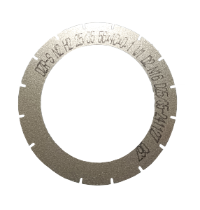
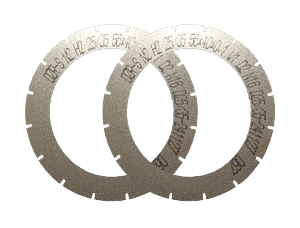
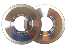
Type Diamond Sawing Blade,Precision Sawing Blade,Semiconductor Sawing Blade,Circular Sawing Blade,Hubbed Sawing Blade,Hubless Sawing Blade,Flanged Sawing Blade,Serrated Sawing Blade,DZY Series Wafer Sawing Blade,DZR Series Sawing Blade,DZR-S Series Slotted Dic Applicable Industry Semiconductor Manufacturing, Semiconductor Packaging, Precision Electronic Component Processing, Optical Ceramic Cutting Params thickness range: 8μm-50μm;
cutting accuracy: ±0.002mm;
spindle speed: 30000-60000rpm;
hardness: HRC 65-70;
bond type: resin/metal;
chip removal rate: ≥1.2mm³/s Scope |
|||||||||
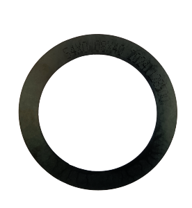
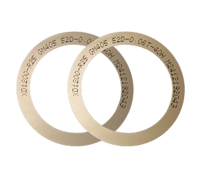
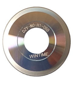
| DB-001 | Diamond Dicing Blade,Precision Dicing Blade,Semiconductor Dicing Blade,Circular Dicing Blade,Hubbed Dicing Blade,Hubless Dicing Blade,Flanged Dicing Blade,Serrated Dicing Blade,DZY Series Wafer Dicing Blade,DZR Series Dicing Blade,DZR-S Series Slotted Dic | Metal bond (for Metal Dicing Blade) Resin bond (for Resin Dicing Blade) Diamond abrasive grains (core functional material) | Semiconductor industry Semiconductor packaging Optical communications New functional materials Functional ceramics Alloy materials Semiconductor packaging components | ||||||
|
Images
Type Diamond Dicing Blade,Precision Dicing Blade,Semiconductor Dicing Blade,Circular Dicing Blade,Hubbed Dicing Blade,Hubless Dicing Blade,Flanged Dicing Blade,Serrated Dicing Blade,DZY Series Wafer Dicing Blade,DZR Series Dicing Blade,DZR-S Series Slotted Dic Applicable Industry Semiconductor industry
Semiconductor packaging
Optical communications
New functional materials
Functional ceramics
Alloy materials
Semiconductor packaging components Params Ultra-thin thickness: ≤9 μm
High precision for wafer cutting
High cutting efficiency for semiconductor packaging
Annual production capacity: Over 1 million pieces
Stable performance for mass production Scope |
|||||||||
Certifications & Compliance
Each record can become a certification entity page.
| Certification | Cert Number | Standard | Authority | Market | Issue Date | Expiry Date | Document |
|---|
Applications & Industries
Taxonomy-backed tags to form industry ↔ supplier ↔ product relationships.
| Industry | Country | Working Condition | Project Type | Function | Operation Mode | Special Requirement | Matched Equipment |
|---|---|---|---|---|---|---|---|
| Semiconductor manufacturing, semiconductor packaging, optical communication, new functional materials, functional ceramics, alloy materials | CN,JP,KR,SG,MY,US,DE | Class 100/1000 clean room, constant temperature (22±2℃), constant humidity (45%-55%), dust-free, anti-static, high-speed spindle environment | Wafer dicing & scribing, semiconductor package cutting, ultra-thin wafer processing, optical device cutting, ceramic substrate cutting, precision alloy component cutting | Realize high-precision wafer cutting, ultra-thin slicing, narrow kerf, low chipping, high-efficiency cutting and stable dimensional control | High-speed spindle rotating cutting, dry/wet cutting, automatic dicing machine continuous operation, precision feeding cutting | Ultra-thin blade thickness ≤9μm, high wear resistance, low cutting loss, anti-static, high dimensional accuracy, long service life, stable mass production | Automatic wafer dicing machine, semiconductor cutting spindle, UV tape mounting machine, wafer cleaning equipment, wafer testing machine |
Industries (1) → Products (2 models) → Certifications (0)
Manufacturing Capabilities
Core processes and equipment available in-house.
Customization
1. Blade diameter, thickness and spindle hole size 2. Bond type (metal bond, resin bond) 3. Diamond abrasive grain size and concentration 4. Coating (anti-rust, heat-dissipation, wear-resistant) 5. Cutting performance (cutting speed, service life) 6. Packaging and special packaging for export 7. Special-shaped blade customization (non-standard size)
Monthly Capacity
800,000+ pieces per month for standard specifications; 80,000+ pieces per month for customized and special-shaped products
Lead Time
2-5 working days for standard products; 10-25 working days for customized orders (adjustable for large orders)
Export Markets
China, Southeast Asia, Middle East, European Union, United States, Canada, Australia, South America, Africa
After Sales
1. Technical support for cutting process matching and equipment adaptation 2. Quality problem investigation and solution within 48 hours 3. Customized after-sales service for bulk procurement customers 4. Long-term supply guarantee and inventory support 5. Product application training for new customers 6. Replacement and compensation for defective products due to quality problems
Quality Control
1. Geometric dimension inspection (vernier caliper, laser diameter gauge) 2. Hardness and wear resistance test (material testing machine) 3. Dynamic balance detection (high-speed dynamic balance tester) 4. Cutting performance simulation test (actual mater
Project References / Cases
Verified project records. Client names anonymized where requested.
| Client Type | Country | Quantity | Application | Duration | Result | Highlight |
|---|---|---|---|---|---|---|
| Semiconductor Packaging Factory | CN | 500,000+ pieces annual usage, mass production line matching | High-precision dicing of 8–12 inch semiconductor wafers for chip packaging | 3 years | Cutting chipping rate ≤5μm, wafer yield increased by 12%, stable mass production without blade replacement | Ultra-thin thickness ≤9μm, narrow kerf, low material loss, long service life |
Comparative Positioning
Side-by-side benchmarks against peer manufacturers in this segment.
| Compared To | Difference | Performance Gap | Best For | Cost Difference | Efficiency |
|---|---|---|---|---|---|
| Traditional resin-bonded dicing blades from mainstream competitors | 1. Ultra-thin blade thickness design (≤9μm) reduces kerf loss 2. Proprietary diamond abrasive formula reduces chipping rate 3. Anti-static coating design for clean room compatibility 4. High wear resistance maintains dimensional stability in mass production 5. Optimized bond structure improves cutting stability for brittle materials (silicon wafer, ceramic) | 1. Kerf width: Our product 9μm vs. Competitor 12μm (25% reduction in material loss) 2. Chipping rate: Our product ≤5μm vs. Competitor ≤10μm (50% lower chipping) 3. Service life: Our product 30% longer than mid-range imported blades 4. Yield rate: Our product improves wafer yield by 12% vs. traditional blades 5. Dimensional accuracy: ±0.001mm tolerance vs. Competitor ±0.003mm | 1. Ultra-thin wafer (8/12 inch) precision dicing 2. High-value semiconductor substrate cutting (SiC/GaN, ceramic, optical glass) 3. Mass production lines with strict requirements for yield and material utilization 4. Clean room Class 100/1000 high-precision manufacturing environments 5. Miniature semiconductor component cutting (MEMS, power devices) | 1. Higher initial purchase cost (10-15%) than standard competitor blades 2. Lower total cost of ownership (TCO) due to 30% longer service life and reduced material waste 3. Reduced downtime from blade replacement lowers production cost by 8% annually | 1. Lower spindle load (15% reduction) during cutting, reducing energy consumption 2. Higher cutting efficiency (20% faster processing speed) under the same power condition 3. Reduced heat generation during high-speed rotation, lowering cooling system energy usage 4. Consistent energy efficiency throughout the product lifecycle (no performance degradation) |
Risk & Trust Signals
Aggregated data-driven indicators. Not an endorsement.
Purchase & Trade Information
Trading terms and procurement details.
Product Comparison
Comparative analysis against alternative solutions.
| Compared To | Difference | Performance Gap | Best For | Cost Difference | Efficiency |
|---|---|---|---|---|---|
| Traditional resin-bonded dicing blades from mainstream competitors | 1. Ultra-thin blade thickness design (≤9μm) reduces kerf loss 2. Proprietary diamond abrasive formula reduces chipping rate 3. Anti-static coating design for clean room compatibility 4. High wear resistance maintains dimensional stability in mass production 5. Optimized bond structure improves cutting stability for brittle materials (silicon wafer, ceramic) | 1. Kerf width: Our product 9μm vs. Competitor 12μm (25% reduction in material loss) 2. Chipping rate: Our product ≤5μm vs. Competitor ≤10μm (50% lower chipping) 3. Service life: Our product 30% longer than mid-range imported blades 4. Yield rate: Our product improves wafer yield by 12% vs. traditional blades 5. Dimensional accuracy: ±0.001mm tolerance vs. Competitor ±0.003mm | 1. Ultra-thin wafer (8/12 inch) precision dicing 2. High-value semiconductor substrate cutting (SiC/GaN, ceramic, optical glass) 3. Mass production lines with strict requirements for yield and material utilization 4. Clean room Class 100/1000 high-precision manufacturing environments 5. Miniature semiconductor component cutting (MEMS, power devices) | 1. Higher initial purchase cost (10-15%) than standard competitor blades 2. Lower total cost of ownership (TCO) due to 30% longer service life and reduced material waste 3. Reduced downtime from blade replacement lowers production cost by 8% annually | 1. Lower spindle load (15% reduction) during cutting, reducing energy consumption 2. Higher cutting efficiency (20% faster processing speed) under the same power condition 3. Reduced heat generation during high-speed rotation, lowering cooling system energy usage 4. Consistent energy efficiency throughout the product lifecycle (no performance degradation) |