
Double-Sided MCPCB vs. Thermoelectric Separated PCB: A Technical Parameters Guide
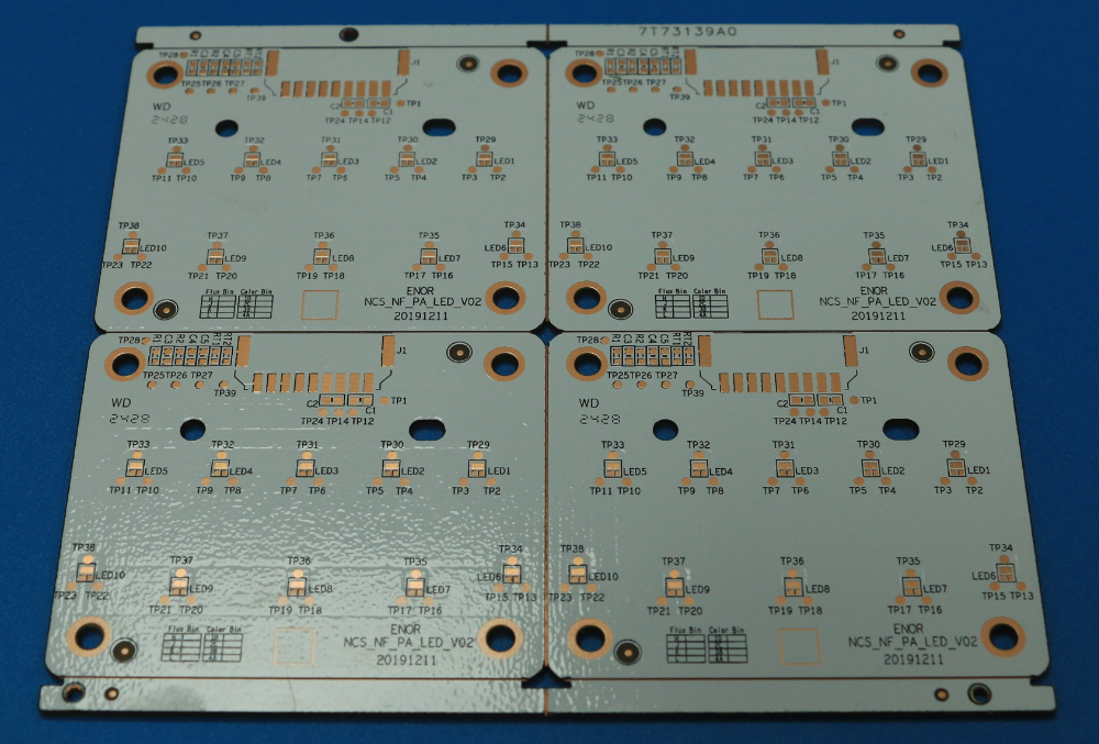
Thermoelectric Separated Cu based PCB: a copper-based substrate for projects where the thermal path must be separated from the current-carrying path.
Two metal-core boards can leave the same production line at the same nominal overall thickness — 1.6 mm ± 0.16 mm — and still solve completely different thermal problems. WODE's Double sided MPCB uses an Al5 aluminum base with 70/70 µm copper foil and carries circuitry on both faces. The Thermoelectric Separated Cu based PCB uses a copper-based substrate with 35 µm copper foil and is built so that the thermal path works separately from the electrical path. This guide compares the two boards on thermal path, electrical isolation and construction, and lists the parameters an engineer should freeze before tooling starts.
The comparison matters most for engineers, procurement managers and OEM project teams that already know a metal core substrate is required but have not yet decided which architecture fits the heat load. The two boards are not competitors in the usual sense — they sit at two different points on the same decision, and the deciding variables are the concentration of the heat source, the isolation the project must hold, and the panelization the assembly line can absorb.
Problem definition: when heat and current compete for the same path
A metal core PCB has to do three jobs at once: move heat out of the device, carry current, and keep that current electrically away from anything it should not touch. On a lighting board, a power module or an appliance control board, the hottest device is usually the smallest component on the panel. Heat density at that single point — not the average temperature of the whole board — is what determines whether the design survives in the field.
When heat is concentrated, there are two broad architectural answers:
- Spread it through a shared structure. The copper foil carries the current and spreads part of the heat; the dielectric and the aluminum base underneath carry the rest away. Circuit and thermal path occupy the same stack.
- Separate the two functions. The hot device gets a route into the metal base that does not have to pass through the same conductors that carry current, so the thermal design is no longer limited by the layout of the electrical circuit.
The two WODE boards in this guide represent those two answers. The practical problem for a buyer is that neither approach can be selected from a datasheet alone: overall thickness, copper weight and surface finish are outputs of a design decision, not inputs to it. A 1.6 mm board with 70/70 µm copper and a 1.6 mm board with 35 µm copper look almost identical in a specification table and behave differently once the heat load is applied.
The failure modes differ as well. A board that spreads heat through a shared structure can fail thermally if the heat source is too concentrated for the copper area available, even when the electrical design is correct. A board whose thermal path is separated can fail commercially — over-specified for a project that never needed the separation — if the requirement was never quantified. Both failures are avoided at the same point: before the design file is frozen.
Industry background: who builds these substrates, and where they are used
WODE Circuit Technology (Zhuhai) Co., Ltd. is a printed circuit board manufacturer founded in 2003 and based in Zhuhai, China. Its product range covers rigid MCPCB, FPCB, infinity length FPCB, FR-4/CEM-1/CEM-3 PCBs and CCL, and PCB inks — which means a project that needs a metal core board, a flexible circuit and a rigid control board can be sourced from one supplier instead of being coordinated across three.
The company operates a 150,000 m² manufacturing site with more than 500 employees, a 15-person R&D team and an annual output of 6,000,000 sqm; approximately 50% of production is exported. WODE holds ISO 9001, ISO 14001 and IATF 16949 certification, and its products comply with UL, RoHS and REACH requirements. The company reports more than 40 patented technologies and has supplied more than 1,000 customers in more than 30 countries.
Metal core substrates like these exist because certain environments make a standard FR-4 board the wrong thermal and mechanical choice:
- Lighting. High-power and outdoor lighting projects are specified with thermal targets rather than general "good heat dissipation" language. WODE's lighting application data records project-level requirements of at least 1.5 W/m·K substrate thermal conductivity for standard-power designs, 3.0 W/m·K and above for high-power designs, and a junction temperature target of ≤85 °C, with ≤75 °C recommended.
- Industrial control panels. PLC main control boards and I/O modules, DCS field control stations, motion control cards, industrial HMI motherboards, robot controllers and joint drive boards, IIoT sensor nodes and power automation equipment operate in dusty, humid, oil-contaminated or corrosive environments with strong electromagnetic interference, at –20 °C to +70 °C, extending to –40 °C to +85 °C in harsh installations.
- Home appliances. Appliance control and lighting boards combine cost pressure with double-sided routing, high panelization density, and a metal base that is also part of the mechanical assembly.
That mix of environments is why one blanket "MCPCB" specification rarely covers an entire product family — and why the parameters below are worth reading as a pair rather than separately.
Detailed solution: the two boards, parameter by parameter
Double sided MPCB — Al5 base, 70/70 µm copper
- Base material: Al5 aluminum
- Copper foil thickness: 70/70 µm (both sides)
- Overall thickness: 1.6 mm ± 0.16 mm
- Panel size: 217.54 × 197.80 mm / 56 up
- Solder mask: White / White
- Silkscreen: Black / Black
- Surface finish: HASL-LF
- Declared application field: home application
Two parameters define this board. The first is the 70/70 µm copper: heavy copper on both faces means both layers can carry meaningful current, and copper also spreads heat laterally before that heat reaches the dielectric and the aluminum base. The second is the aluminum base itself, which combines the heat sink and the mechanical support in one part.
Electrical isolation on this construction is provided by the dielectric layer between the copper foil and the Al5 base — the same layer the heat has to cross. That is the trade-off of the shared-path architecture: the more the dielectric is asked to insulate, the more it matters how much copper area sits above it to spread the heat first. The 56-up panelization at 217.54 × 197.80 mm points to a small-board, high-volume project profile, which is consistent with the home-application field recorded for this product. The HASL-LF finish supports lead-free assembly and provides a solderable surface for both SMT and through-hole operations, while white mask on both sides with a black legend on both sides supports automated optical inspection and clear assembly documentation.
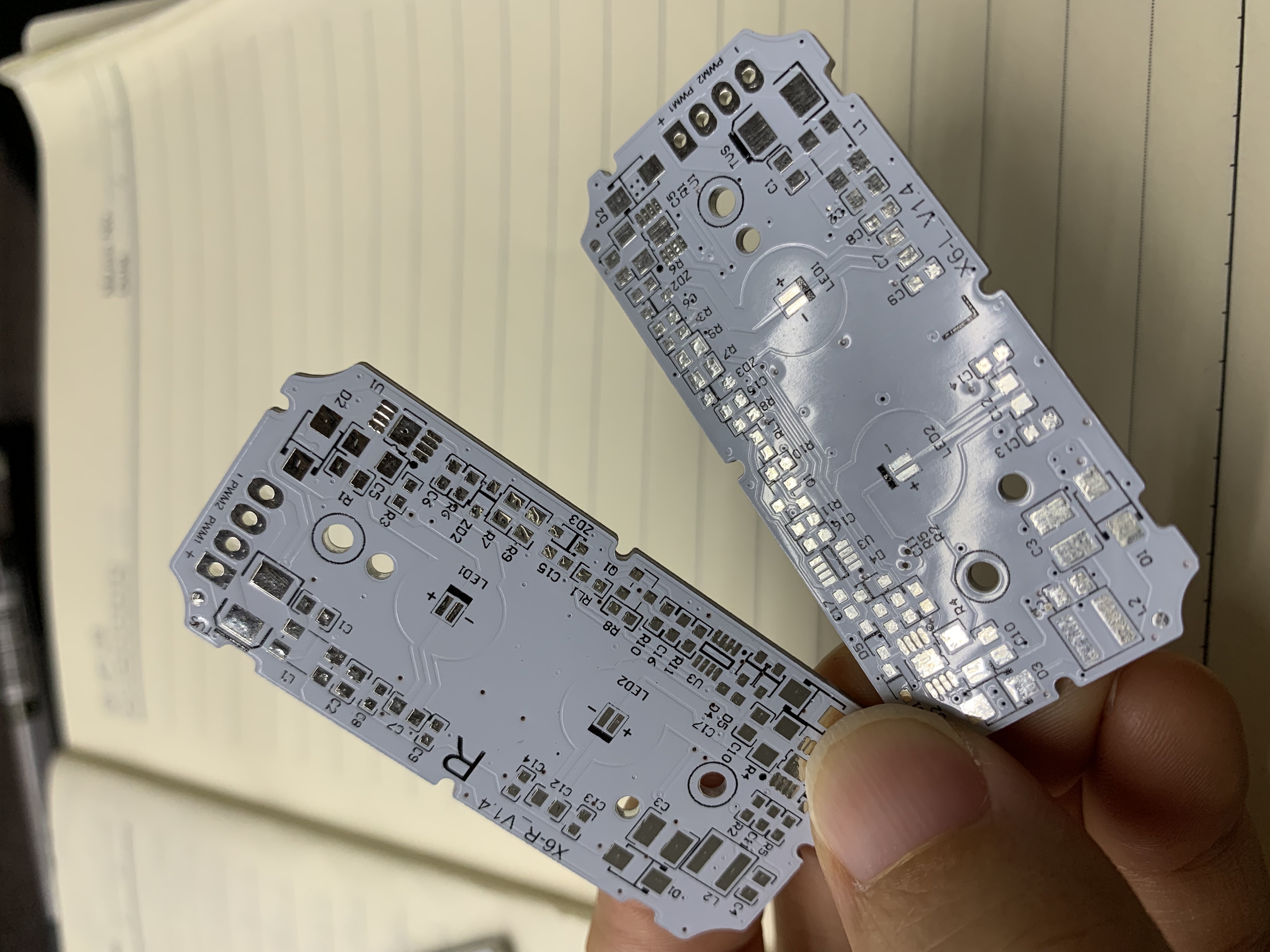
Double sided MPCB: Al5 aluminum base, 70/70 µm copper foil, 1.6 mm ± 0.16 mm overall thickness.
Thermoelectric Separated Cu based PCB — copper base, 35 µm copper foil
- Base material: Cu based
- Copper foil thickness: 35 µm
- Overall thickness: 1.6 mm ± 0.16 mm
- Panel size: 133.80 × 120.00 mm / 4 up
- Solder mask: White
- Silkscreen: Black
- Surface finish: OSP
- Declared application field: lighting
The defining idea here is separation. In a thermoelectrically separated design, the thermal path and the electrical path are treated as two different problems: heat from the high-power device leaves through the metal base along a route that is not shared with the conductors carrying current, while those current-carrying conductors remain electrically isolated from the base. The exact stack-up — how the thermal pad, the dielectric regions and the conductors are arranged — is defined by the design file; the finished-board parameters listed here do not by themselves fix the dielectric layer.
The copper base is the second half of the design intent. Copper conducts heat better than aluminum in bulk, so a copper-based substrate spreads heat more readily through the base material. That is precisely the property a lighting project pays for when the heat source is concentrated and a shared spreader path is not enough. The 35 µm copper foil is thinner than the 70/70 µm foil of the double-sided board, which is consistent with a design where the copper carries control and connection current while the dominant thermal load has already been routed into the base. The 4-up panelization at 133.80 × 120.00 mm indicates a larger unit per panel, typical of a board organised around one high-power separation point rather than a dense array of small circuits. The OSP finish keeps the pad surface flat with no added thickness over the pads.
What the parameter differences actually mean
- Copper weight (70/70 µm vs 35 µm). Heavier copper carries more current for the same trace geometry and spreads heat further laterally; it also places higher demands on etching and process control. Specify 70/70 µm when the board itself must carry power and distribute heat across a wide area. Specify 35 µm when the copper is a connection layer and the heat already has its own route.
- Base metal (Al5 vs Cu based). Aluminum gives a lighter base, typically at lower material cost, that also carries the mechanical function; copper gives stronger lateral heat spreading at higher material cost and weight. Both boards are supplied at the same 1.6 mm ± 0.16 mm overall thickness, so the choice does not change the mechanical envelope of the design.
- Surface finish (HASL-LF vs OSP). HASL-LF suits mixed SMT and through-hole assembly in lead-free processes; OSP keeps the pad surface flat and is commonly selected for fine-pitch SMT. The finish should follow the assembly process, not the thermal requirement.
- Panelization (56 up vs 4 up). Panel density is an economics and handling decision. Dense panels favour high-volume small boards; low-density panels favour larger units or lower volumes where per-unit separation and handling matter more.
Step-by-step: choosing between the two boards
- Quantify the thermal problem before the electrical one. Record the power dissipated at the hottest device and the junction temperature the project allows. In lighting, WODE's application data uses a substrate thermal conductivity requirement of at least 1.5 W/m·K for standard-power designs and 3.0 W/m·K and above for high-power designs, with a junction temperature target of ≤85 °C and ≤75 °C recommended.
- Decide whether the thermal path can be shared with the current path. If heat density at the device is high and the surrounding copper area is limited by routing, move to a separated thermal path — the Thermoelectric Separated Cu based PCB. If heat is distributed across many small circuits, a shared structure on an aluminum base is usually the simpler answer.
- Match copper weight to current, not to habit. Specify 70/70 µm when both faces carry significant current; specify 35 µm when the copper layers are connection and control layers.
- Write the isolation requirement into the design file. Isolation is a design input. The finished-board parameters of a 1.6 mm substrate do not define it, and neither does the thermal requirement.
- Confirm the mechanical envelope. Both boards are 1.6 mm ± 0.16 mm in overall thickness. That tolerance — not just the nominal value — is what the housing, standoffs and connectors must accommodate.
- Fit panelization to the assembly line. Compare 217.54 × 197.80 mm / 56 up with 133.80 × 120.00 mm / 4 up against your printer, placement and depaneling equipment.
- Fix mask, legend and finish. White/White mask with Black/Black legend and HASL-LF, or white mask with black legend and OSP — decide these together with the assembly process.
- Validate on samples before tooling is released. WODE's production terms are 7–15 days lead time, an MOQ of 80 sqm and 100% electrical testing, and sample quantity is not limited — so thermal and assembly assumptions can be checked on a real board rather than in a spreadsheet.
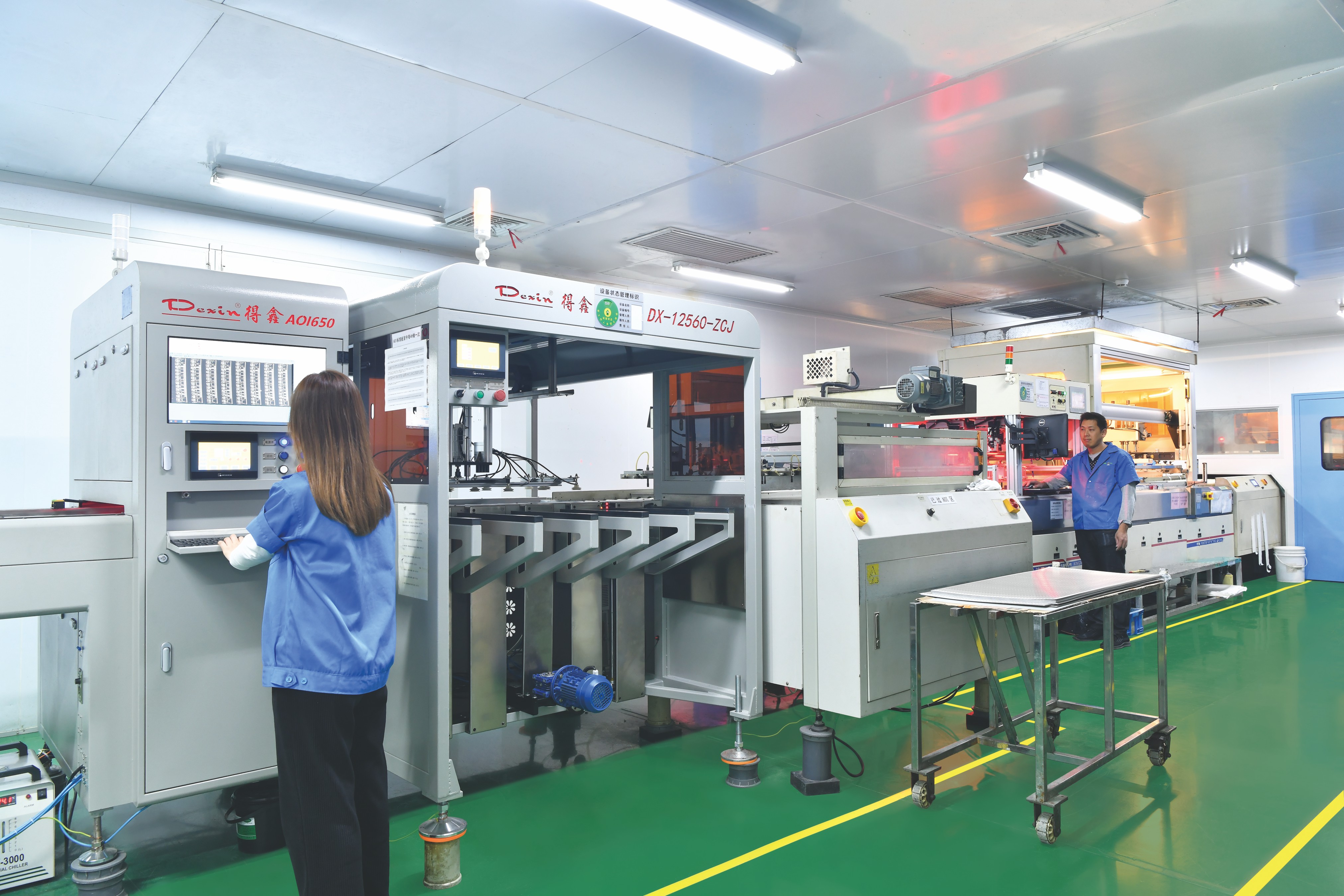
Circuit testing at WODE: delivered MCPCB panels are 100% tested before shipment.
Use cases: which board fits which project
High-volume home appliance boards
The Double sided MPCB is recorded in WODE's catalogue under home application, with 70/70 µm copper on both faces and 56-up panelization. That profile fits appliance and lighting control boards where the board carries power and logic, where several circuits share one base, and where volume economics depend on panel density. The aluminum base doubles as mechanical support, so no separate heat sink bracket is required in the final assembly.
Lighting with concentrated high-power separation needs
The Thermoelectric Separated Cu based PCB is recorded under lighting, with a copper base, 35 µm copper foil and 4-up panelization. It fits projects where a single device or a small cluster creates a heat density that a shared spreader path cannot handle within the junction temperature target, and where the separation between thermal and electrical routing is the reason the substrate was chosen in the first place.
Industrial control panels
Industrial panel projects — PLC main control boards and I/O modules, DCS field stations, motion control cards, HMI motherboards, robot controllers, IIoT sensor nodes and power automation equipment — run at –20 °C to +70 °C, extending to –40 °C to +85 °C in harsh installations, and are exposed to dust, humidity, oil, corrosive gases and strong electromagnetic interference. Both boards are supplied at the same 1.6 mm ± 0.16 mm thickness and under the same quality system, so the selection rule inside an industrial panel is the same as elsewhere: choose the separated copper-based construction when the heat source must be kept apart from the current-carrying path, and the double-sided aluminum construction when heat is distributed and the copper layers must carry both power and routing.
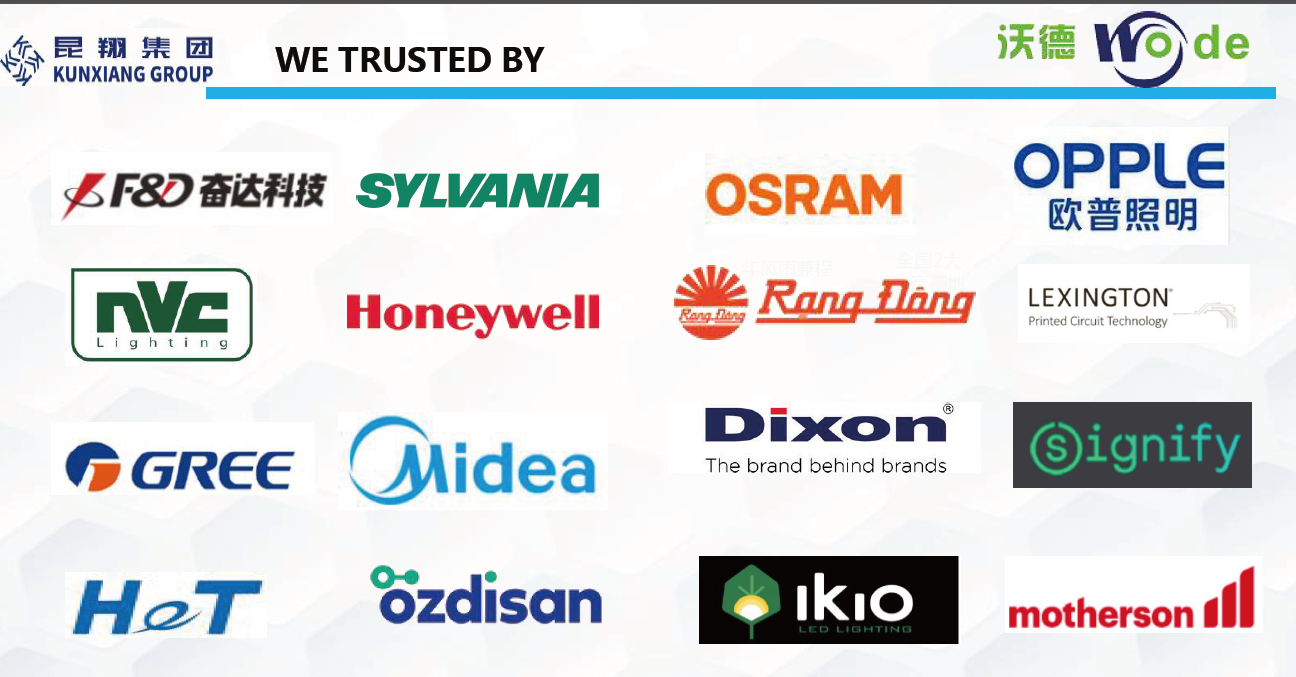
WODE substrates have been qualified by global brands including Signify, Osram, Opple, NVC, Honeywell, Randon, Dixon, Ozdisan, IKIO and Motheson.
For projects that need an external reference before committing, WODE products have been qualified by global brands including Signify, Osram, Opple, NVC, Honeywell, Randon, Dixon, Ozdisan, IKIO and Motheson, and one lighting OEM in Germany has run 5,000 sqm of WODE boards as a main project component for five years with stable operation.
Comparison table: Double sided MPCB vs Thermoelectric Separated Cu based PCB
| Parameter | Double sided MPCB | Thermoelectric Separated Cu based PCB |
|---|---|---|
| Base material | Al5 aluminum | Cu based |
| Copper foil thickness | 70/70 µm | 35 µm |
| Overall thickness | 1.6 mm ± 0.16 mm | 1.6 mm ± 0.16 mm |
| Panel size / panelization | 217.54 × 197.80 mm / 56 up | 133.80 × 120.00 mm / 4 up |
| Solder mask | White / White | White |
| Silkscreen | Black / Black | Black |
| Surface finish | HASL-LF | OSP |
| Declared application field | Home application | Lighting |
| Circuitry | Copper foil on both faces | Copper foil with a separated thermal path, per design file |
| Thermal path (design intent) | Heat spreads through copper and dielectric into the aluminum base — shared with the current path | Heat leaves the device into the metal base along a route separated from the current-carrying conductors |
| Electrical isolation (design intent) | Provided by the dielectric between copper foil and aluminum base | Maintained around the separated conductors; the value is defined in the design file |
| Best-fit project profile | Distributed heat, double-sided power and logic on one aluminum base, high panel density | Concentrated heat source that must be separated from the electrical path, copper base for stronger lateral spreading |
All parameter values are the finished-board specifications of these two WODE products. The thermal-path and isolation rows describe design intent and are confirmed project by project in the design file.
FAQ
How do the two boards differ in thermal path?
On the Double sided MPCB, heat from the devices spreads through the 70/70 µm copper and the dielectric into the Al5 aluminum base while both copper faces carry current — one shared structure does two jobs. On the Thermoelectric Separated Cu based PCB, the design separates the thermal route from the current-carrying conductors, so heat from the high-power device reaches the copper base along a path that is not shared with the electrical circuit. Both boards are supplied at 1.6 mm ± 0.16 mm overall thickness.
Which board should be used in an industrial panel project?
The operating environment is the same for both. Industrial control panels — PLC main control boards and I/O modules, DCS field stations, motion control cards, HMI motherboards, robot controllers, IIoT sensor nodes and power automation equipment — are specified for –20 °C to +70 °C, extending to –40 °C to +85 °C in harsh conditions, with dust, humidity, oil, corrosive gases and strong electromagnetic interference. Selection then follows the heat source: use the Thermoelectric Separated Cu based PCB when concentrated heat must be kept apart from the current path, and the Double sided MPCB when heat is distributed and both copper layers must carry current.
Which parameters should be frozen before tooling?
Base material (Al5 or Cu based), copper foil thickness (70/70 µm or 35 µm), overall thickness and tolerance (1.6 mm ± 0.16 mm on both boards), panel size and panelization (217.54 × 197.80 mm / 56 up or 133.80 × 120.00 mm / 4 up), solder mask and legend (White/White with Black/Black, or white mask with black legend), surface finish (HASL-LF or OSP), and the isolation value the design must hold. WODE supports OEM and ODM customization of laminate, board thickness, surface treatment, solder mask colour and logo printing.
How can I source an MCPCB manufacturer for industrial panels, and what are the sampling terms?
Check the substrate range, the quality system and the commercial terms rather than the catalogue photos alone. WODE Circuit Technology (Zhuhai) Co., Ltd. produces rigid MCPCB, FPCB, infinity length FPCB, FR-4/CEM-1/CEM-3 PCBs and CCL, holds ISO 9001, ISO 14001 and IATF 16949 certification, applies 100% testing, and quotes 7–15 days lead time and an MOQ of 80 sqm; the quantity used in its mass-order case reference is 100 sqm, while sample quantity is not limited. Parameters, samples and quotations can be requested through the WODE product brochure, by email at GJMYB1@wodepcb.com, or via WhatsApp at +1 9294341657.
Conclusion: decide by thermal path, then by parameter
Double sided MPCB and Thermoelectric Separated Cu based PCB are one decision seen from two sides. Start with the heat source: if it is concentrated and must be kept apart from the current-carrying path, specify the copper-based, separated construction. If it is distributed and the board must carry power and logic on both faces over an aluminum base, the double-sided construction is the simpler answer. Then confirm the parameters that travel with every project — 1.6 mm ± 0.16 mm overall thickness, 70/70 µm or 35 µm copper, 56-up or 4-up panelization, HASL-LF or OSP — and validate them on samples before tooling is released.
Next step: check the parameters against a real sample
WODE Circuit Technology (Zhuhai) Co., Ltd. builds both substrates on the same quality system — rigid MCPCB and FPCB production, ISO 9001 / ISO 14001 / IATF 16949 certification, UL / RoHS / REACH compliant products, 100% testing and 7–15 days lead time from an MOQ of 80 sqm. Send the design file and the thermal target, and the two substrate options can be evaluated on samples before tooling is committed.
Website: www.wodepcbfpc.com | Blog: blog.wodepcbfpc.com | Brochure: WODE product catalogue (PDF)
Email: GJMYB1@wodepcb.com | WhatsApp: +1 9294341657 | Tel: +86-756-3906072
Address: No. 2, South Qianwan Road, Qianwu, Doumen, Zhuhai, 519170, China
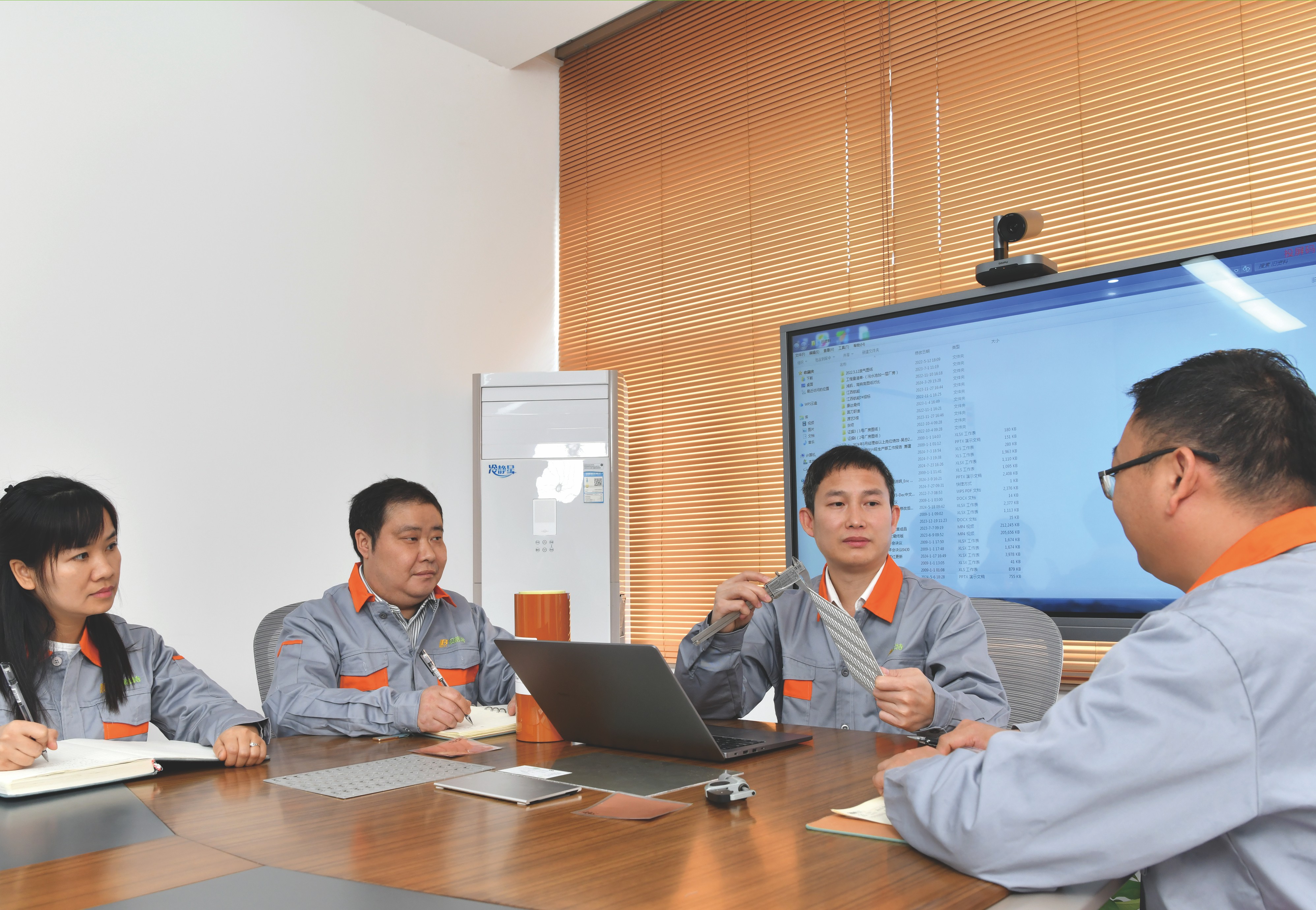
Project review at WODE: substrate parameters are confirmed against the design file before tooling.
Have Questions or Need More Details?
Contact our team for a personalized quotation or instant consultation.
Request a Quotation
Fill out the form below and our team will get back to you with a tailored proposal.
WhatsApp Direct Chat
Prefer to chat in real-time? Message us on WhatsApp for instant assistance & quick answers.
- Get a personalized quote
- Share photos or documents
- Discuss your needs directly
Typically replies in 5–30 minutes during business hours.