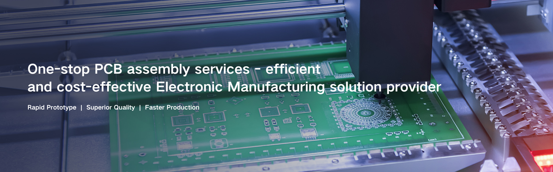
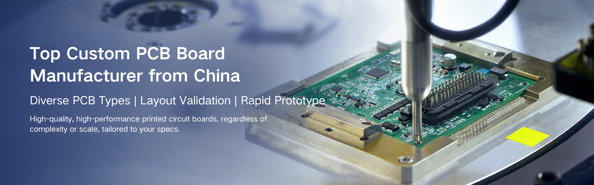
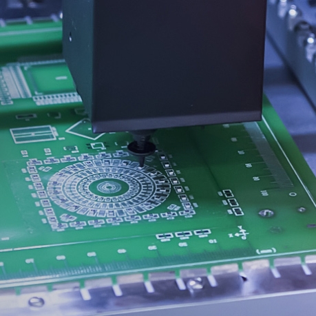
Benefit from Our Advanced PCB Manufacturing Techniques
Start a collaboration that perfectly combines affordability, flexibility, adaptability, and the efficiency of direct factory access.
Number of Layers
From simple 2-layer boards to complex stacks of over 64 layers. More layers allow for more intricate routing.
Minimum Trace/Spacing
Our manufacturing processes reliably produce ultra-fine traces and spaces of 3mil, enabling intricate and spacious designs.
Via Process
Plated through-holes, microvias, buried vias, and stacked vias ensure seamless interconnection for smooth layer transitions in multilayer designs.
Plating and Surface Finish
Lead-free HASL, immersion gold (ENIG), immersion silver, immersion tin, OSP, hard gold, solder plating, and more.
Customization and Testing
Our capabilities include custom colors for solder masks and silkscreen for clear labeling, backed by rigorous testing methods such as AOI and X-ray inspection to ensure quality