How Semicera Builds OEM Semiconductor Process Materials
How Semicera Builds OEM Semiconductor Process Materials
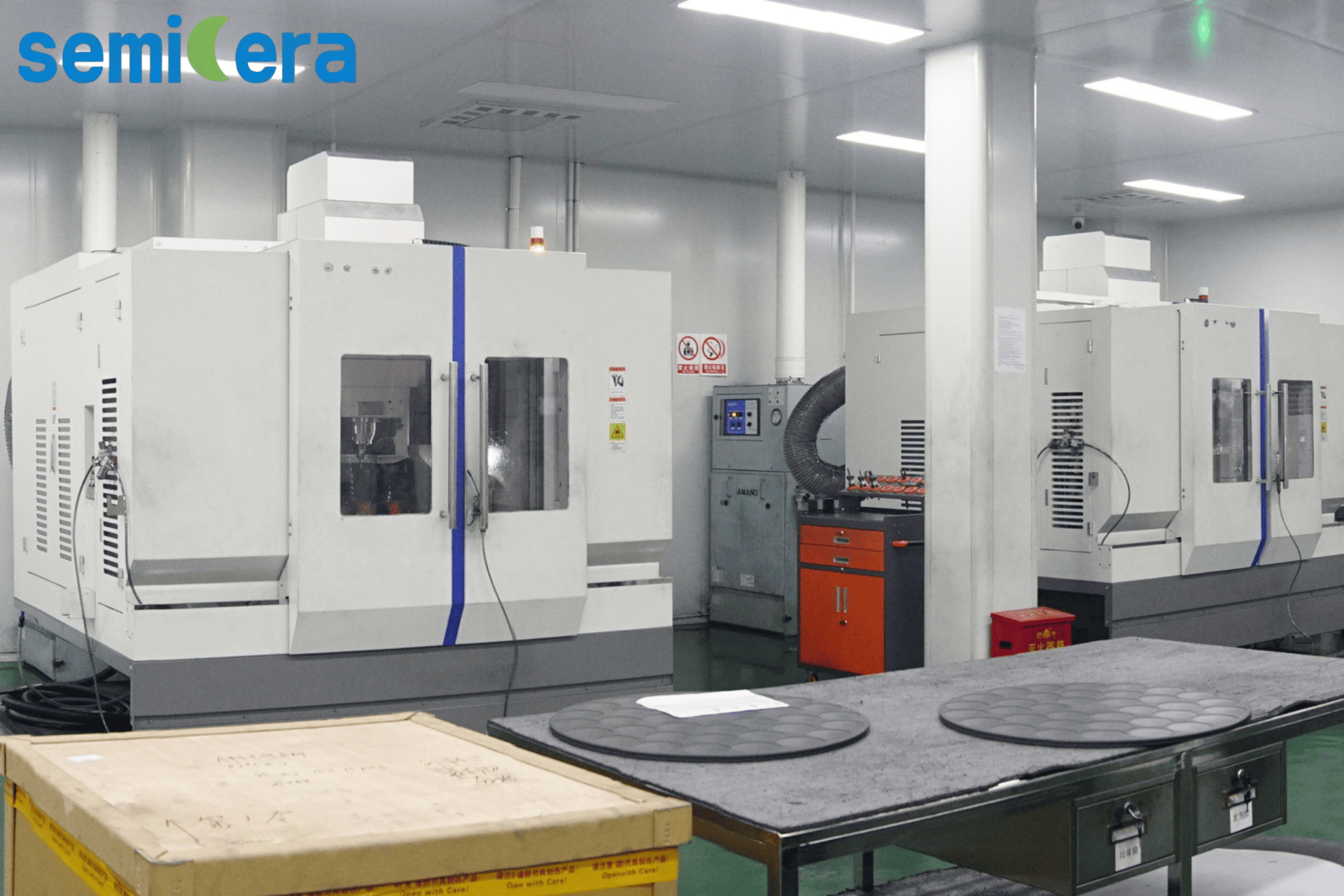
Semicera is a semiconductor materials and components manufacturer headquartered in Ningbo, China, that designs and produces OEM semiconductor process materials for epitaxy, etch, oxidation/diffusion, and silicon carbide crystal growth. Founded in 2015, Semicera operates a 40,000 m² manufacturing base with 600+ employees and an annual output of 120,000 units. This article explains what Semicera's OEM capability includes, which materials and processes are covered, and what buyers should verify when moving from supplier evaluation to order execution.
The Procurement Problem: Process Materials Are Not Off-the-Shelf Commodities
In semiconductor fabrication, process materials are the components that sit inside wafer processing equipment: MOCVD susceptors and trays, etch rings, wafer boats, furnace tubes, paddles, insulation felts, heaters, and crystal-growth crucible structures. These components operate at high temperature, in reactive gas atmospheres, and under plasma conditions. Their purity, coating integrity, and dimensional accuracy affect epitaxial uniformity, particle counts, wafer yield, and equipment uptime.
For buyers at the evaluation-to-execution stage, the decision is not limited to material grade. It also depends on whether a supplier can engineer, machine, coat, inspect, and deliver a component that matches the buyer's process conditions and production schedule. A catalog item with the right product name is not sufficient; the supplier must demonstrate process-specific capability, quality control, and commercial flexibility.
Industry Background: A $67.5 Billion Materials Market
The global semiconductor materials market reached $67.5 billion in revenue in 2024, a 3.8% increase over the previous year, according to SEMI. Wafer fabrication materials, the segment that includes process chemicals and CVD materials, grew 3.3% to $42.9 billion in the same year (SEMI). Several component categories relevant to this article also expanded. The global semiconductor graphite market was valued at approximately $1.62 billion in 2024 and is projected to grow at a CAGR of 7.2% through 2032 (Verified Market Reports). SiC-coated graphite susceptors, which are critical for epitaxial growth, were valued at approximately $350 million in 2024 (Valuates Reports). Quartz fabricated parts used in semiconductor manufacturing reached approximately $2.21 billion in 2024, with 5.5% annual growth (TECHCET).
Two technical trends shape supplier evaluation. First, CVD SiC coating is the dominant protection method for graphite susceptors in MOCVD and epitaxial reactors, due to its high purity and thermal conductivity (Dataintelo). Second, tantalum carbide (TaC) coatings are gaining traction for ultra-high-temperature processes such as SiC crystal growth. Buyers therefore need a supplier that controls the full material chain: substrate, coating, precision machining, and inspection.
Semicera's OEM Capability for Semiconductor Process Materials
Semicera (Ningbo Miami Advanced Material Technology Co., Ltd.) is a semiconductor materials and components manufacturer integrating R&D, production, and global sales. The company operates dual research centers, three large-scale production bases, and more than 50 advanced production lines. The R&D team includes more than 100 engineers, representing over 25% of the workforce, and about 40% of output is exported to the EU, the US, and Asia.
Product Portfolio and Material Families
Semicera's main products are CVD SiC coating parts, CVD TaC coating parts, CVD PyC coating parts, SiC ceramic parts, semiconductor advanced ceramic parts, quartz parts, carbon fiber parts, and CFC material. These products serve LED, IC integrated circuits, third-generation semiconductors, epitaxy, MOCVD, CVD, and photovoltaic applications.
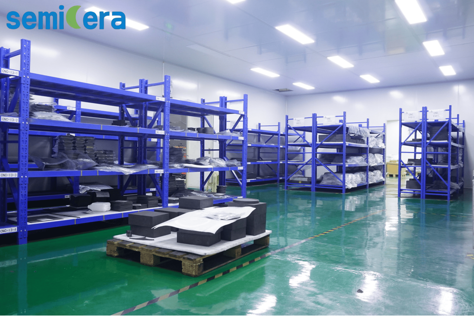
The product family includes SiC-coated graphite susceptors, TaC-coated diversion rings, SiC wafer boats, semiconductor quartz parts, and high-purity graphite components with impurity levels below 5 ppm. The hot-zone range also includes wafer boats, susceptors, preheat rings, furnace tubes, furnace thermal field materials, rigid felt, soft felt, and CFC components such as heaters, bolts, and crucibles.
Process Coverage
Semicera's OEM process materials map to specific process steps as follows:
Epitaxy / MOCVD / RTP: CVD SiC-coated graphite carriers (model CVD-01) and CVD TaC-coated graphite carriers (model CVD-02), used as MOCVD multi-pocket wafer susceptors and trays.
Etch: etch rings (focus or edge rings) made of pure CVD solid SiC or high-purity silicon single crystal.
Oxidation / diffusion / LPCVD: quartz wafer boats, quartz furnace tubes, SiC wafer boats (SiC-01), SiC furnace tubes (SiC-02), and SiC paddles (SiC-03).
Silicon carbide crystal growth (PVT): CVD solid SiC parts (CVD-03), CVD SiC particle (CVD-04), and TaC-coated carriers for ultra-high-temperature operation.
Silicon / SiC crystal growth hot zone: semiconductor rigid felt, semiconductor soft felt, and CFC material for heaters, bolts, and crucibles.
General process support: semiconductor graphite, supplied as ultra-fine-grain isostatic graphite blocks and machined parts.
Coating and Purity Parameters
Coating quality is central to Semicera's epitaxy and high-temperature components. The CVD SiC coating is specified with a typical thickness of 100 µm (range 50–150 µm), a purity level of 99.99995% (6N grade, total ash ≤5 ppm), and a coating hardness of 2500 Vickers (40 GPa); the crystal structure is FCC beta-phase polycrystal with (111) orientation. The CVD TaC coating uses a cubic tantalum carbide matrix with a typical thickness of 25–45 µm, operates up to 2200°C, and has outstanding resistance to ammonia (NH3) and hydrogen (H2) etching.
For structural applications, CVD solid SiC parts reach a density of ≥3.21 g/cm³ with 0% porosity and thermal conductivity ≥150 W/m·K. Etch rings hold total metal purity below 5 ppb and a flatness tolerance of 10 µm or better. Quartz components use GE214 or equivalent ultra-high-purity fused quartz with SiO2 content ≥99.99% and hydroxyl content below 20 ppm. High-purity graphite components are machined from ultra-fine-grain isostatic graphite with grain size 2–5 µm and ash content ≤5 ppm.
Quality and Compliance
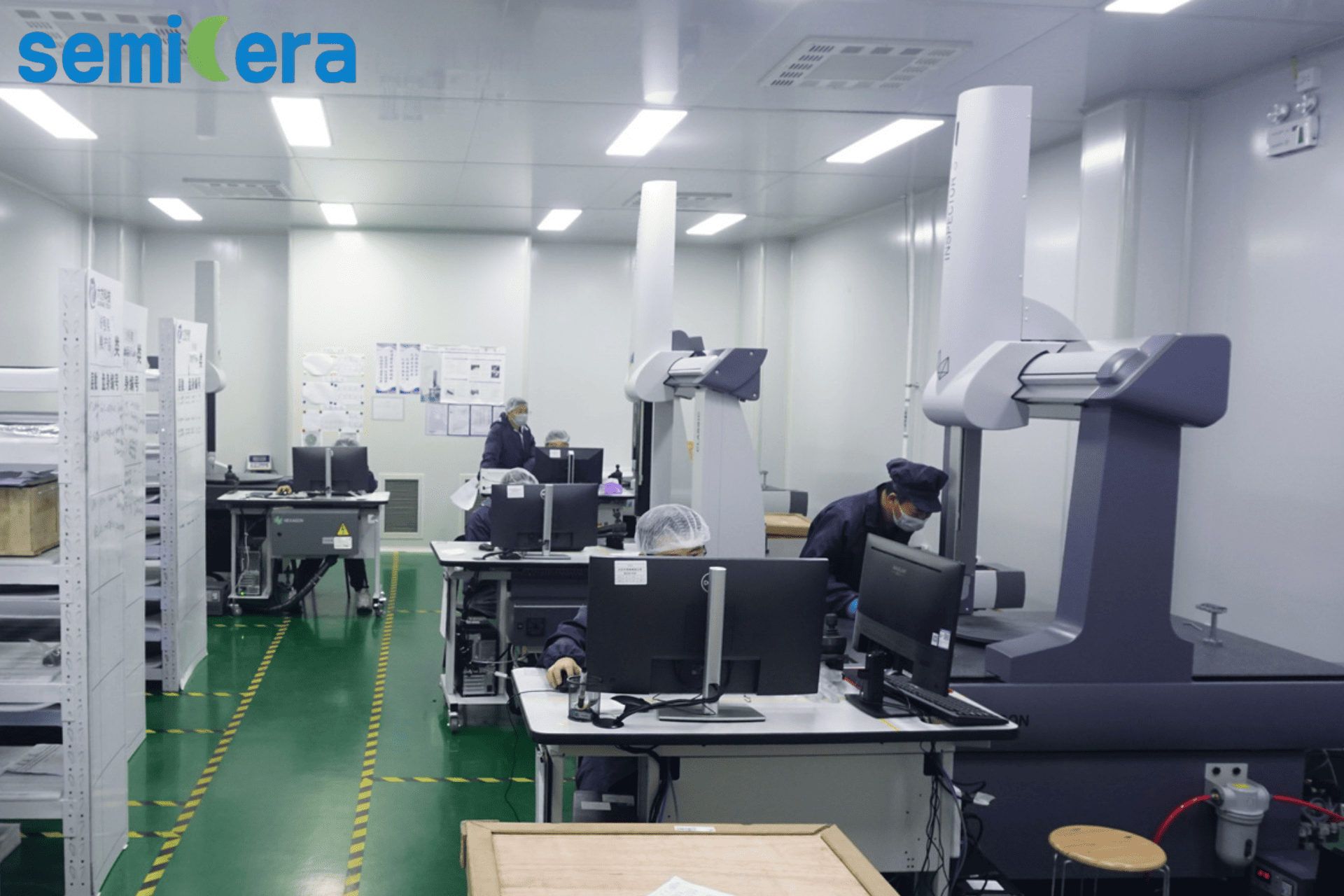
Semicera operates under ISO 9001, ISO 14001, and ISO 45001 quality management system certificates, each with a global market scope and a certification period from 1 December 2025 to 1 December 2026. All OEM production is subject to 100% testing, and commercial acceptance is based on a pre-shipment test.
OEM and Commercial Terms
OEM services at Semicera include customization of voltage and logo. The minimum order quantity is 1 unit, and monthly OEM capacity exceeds 10,000 units. Typical production lead time is 30–50 days. Delivery terms can be quoted as EXW, FCA, DAP, or DDP. Payment for new customers is 100% T/T in advance; long-term cooperation customers pay 70% T/T in advance and 30% before shipment. After-sales remote support is available for EU, US, and Asian markets.
Download the Semicera Product Catalog
The catalog covers CVD SiC / TaC / PyC-coated parts, SiC ceramics, semiconductor quartz, high-purity graphite, CFC material, and hot-zone components.
Step by Step: How an OEM Process Material Program Runs
Semicera's OEM process material program follows a specification-to-shipment sequence. The buyer and the Semicera engineering team align on the following points before production begins.
- Define the process and component function. Identify the target process (epitaxy, etch, oxidation/diffusion, or crystal growth) and the component type: susceptor, wafer boat, furnace tube, etch ring, paddle, felt, or CFC structure.
- Set the material and purity grade. Select the substrate family: isostatic graphite, CVD SiC, SiSiC/RSiC, quartz, or carbon-fiber composite. Confirm the required purity, such as graphite ash ≤5 ppm, CVD SiC 99.99995%, or quartz SiO2 ≥99.99%.
- Confirm the coating specification. Choose CVD SiC (50–150 µm), CVD TaC (25–45 µm, up to 2200°C), PyC coating, or an uncoated material based on operating temperature and gas chemistry.
- Verify dimensional and mechanical limits. Check tolerances such as quartz boat slot pitch ±0.05 mm, SiC furnace tube wall thickness ±0.2 mm, SiC paddle deflection ≤2.0 mm at maximum reach, and etch ring flatness ≤10 µm.
- Review quality control. Semicera performs 100% testing during production and pre-shipment testing before delivery, under ISO 9001, ISO 14001, and ISO 45001 systems.
- Align commercial terms. MOQ is 1 unit; monthly OEM capacity exceeds 10,000 units; typical production lead time is 30–50 days; delivery can be quoted as EXW, FCA, DAP, or DDP.
- Plan support and repeat supply. After-sales remote support is available, and long-term cooperation customers are offered extended payment terms of 70% T/T in advance and 30% before shipment.
Field Experience: Semicera Process Materials in Production
Semicera's process materials are supplied in repeat production programs across North America, Asia-Pacific, and Europe. The following cases summarize the application, volume, operating duration, and reported results.
Epitaxy process components — 900 units/month
Application: epitaxy process, over 2 years under continuous high-temperature conditions.
Result: stable mass production with consistent epitaxial uniformity; equipment maintenance downtime reduced by 15%.
Highlights: high-density CVD coating, thermal shock resistance, strict dimensional tolerances, high ROI.
Epitaxy process components — 200 units/month
Application: epitaxy process, over 2 years under continuous high-temperature conditions.
Result: flawless mass production with ultra-low particle counts; overall wafer yield increased by 2.5%.
Highlights: coating thickness uniformity, thermal conductivity, ultra-low particle generation, long lifespan.
Epitaxy process components — 500 pcs/month
Application: epitaxy process, over 2 years under continuous high-temperature conditions.
Result: stable mass production with consistent epitaxial layer quality; edge ring replacement frequency reduced by 20%.
Highlights: high-density CVD coating, fluorine/chlorine plasma resistance, zero coating peeling under rapid thermal cycling.
CFC insulation for silicon single crystal furnace — 1,000 units/year
Application: insulation for silicon single crystal furnace, over 2 years under continuous high-temperature conditions.
Result: significant energy efficiency improvements; excellent hot-zone temperature uniformity across the pulling process.
Highlights: 3D needle-punched carbon composite matrix, tensile strength, low thermal conductivity, zero structural deformation.
SiC crystal growth materials — 10,000 units/year
Application: high-quality SiC crystal growth, over 2 years under continuous high-temperature conditions.
Result: stable mass production with consistent SiC crystal growth quality; process downtime reduced by 15%.
Highlights: ultra-high-purity matrix coating, thermal shock resistance, zero outgassing, long-term stability under 2000°C operation.
Material Selection Table: Matching Material to Process
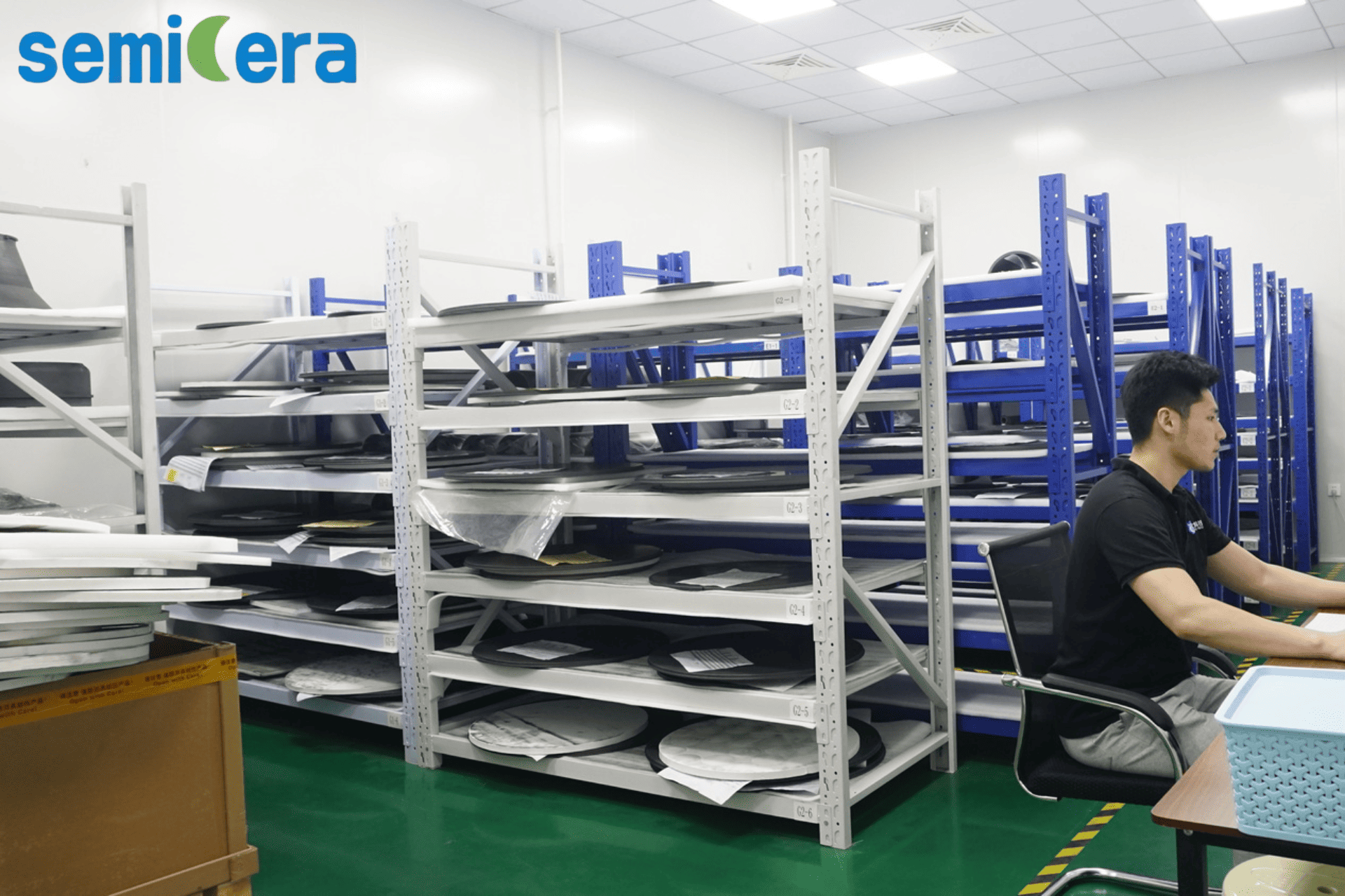
The table below summarizes Semicera's material families by representative specification and typical application. It is a first reference for selecting semiconductor process materials.
| Material / component | Representative parameters | Typical application |
|---|---|---|
| High-purity isostatic graphite | Grain 2–5 µm; ash ≤5 ppm; flexural strength 45–65 MPa; CTE 4.0–4.6×10⁻⁶ K⁻¹ | Wide range of semiconductor processes |
| CVD SiC-coated graphite carrier (CVD-01) | Coating 50–150 µm (typical 100 µm); purity 99.99995%; hardness 2500 Vickers; beta-phase polycrystal (111) | MOCVD epitaxy / RTP |
| CVD TaC-coated graphite carrier (CVD-02) | Coating 25–45 µm; operation up to 2200°C; NH3/H2 resistant; cubic TaC matrix | Epitaxy, ultra-high-temperature processes |
| CVD solid SiC parts (CVD-03) | Density ≥3.21 g/cm³; 0% porosity; thermal conductivity ≥150 W/m·K | SiC crystal growth, dummy wafers |
| CVD SiC particle (CVD-04) | Purity ≥99.9999% (metals <1 ppm); grain 1.0–5.0 mm; free carbon ≤0.05 ppm | PVT SiC crystal growth raw material |
| Etch ring | Plasma erosion <2 nm/min (CF4/O2); flatness ≤10 µm; total metals <5 ppb | Plasma etch process |
| Quartz wafer boat / quartz furnace tube | SiO2 ≥99.99%; OH <20 ppm; 1150°C continuous, 1300°C short-term; slot pitch ±0.05 mm | Oxidation / diffusion |
| SiC wafer boat / furnace tube / paddle | Up to 1600°C; lifespan >5× quartz boats; wall thickness ±0.2 mm; tube length up to 3000 mm | LPCVD / oxidation / diffusion |
| CFC material, rigid felt, soft felt | CFC tensile 90–140 MPa; density 1.65–1.78 g/cm³; felt ash ≤20 ppm (ultra ≤5 ppm); processing up to 2500°C | Crystal growth hot-zone insulation and structures |
One limitation worth noting: OEM material performance depends on the accuracy of the buyer's specification. Process temperature, gas chemistry, and component dimensions determine material and coating selection, and Semicera's pre-shipment test is the formal acceptance gate before delivery. Buyers should finalize the drawing and parameter sheet before production begins.
FAQ
Which quality and management certifications does Semicera hold for semiconductor process material manufacturing?
Semicera holds ISO 9001, ISO 14001, and ISO 45001 quality management system certificates with a global market scope, valid from 1 December 2025 to 1 December 2026. All OEM production is subject to 100% testing, and shipments are accepted based on pre-shipment inspection.
Which semiconductor processes do Semicera's OEM process materials cover?
Semicera's OEM materials cover epitaxy/MOCVD and RTP processes (CVD SiC-coated and TaC-coated graphite carriers), etch processes (CVD SiC or high-purity silicon etch rings), oxidation/diffusion and LPCVD processes (quartz and SiC wafer boats, furnace tubes, paddles), and silicon/silicon carbide crystal growth (CVD SiC parts, CVD SiC particle, CFC material, rigid felt, soft felt). Products are used in LED, IC integrated circuits, third-generation semiconductors, epitaxy, MOCVD, CVD, and photovoltaic applications.
What OEM customization options does Semicera offer for semiconductor components?
Semicera OEM services include customization of voltage and logo. The minimum order quantity is 1 unit, monthly OEM capacity exceeds 10,000 units, quality control is 100% testing, and after-sales remote support is available for EU, US, and Asia markets.
Which purity and coating parameters should buyers verify in semiconductor process materials?
Buyers should verify substrate purity and coating specification. Semicera's high-purity graphite has ash content below 5 ppm; CVD SiC coating is typical 100 µm (range 50–150 µm) at 99.99995% purity with 2500 Vickers hardness; TaC coating is typical 25–45 µm with operation up to 2200°C; etch rings hold total metal purity below 5 ppb; quartz components have SiO2 content ≥99.99%.
What are Semicera's MOQ, payment terms, and delivery options?
Semicera's MOQ is 1 unit. Delivery can be quoted as EXW, FCA, DAP, or DDP. New customers pay 100% T/T in advance; long-term cooperation customers pay 70% T/T in advance and 30% before shipment. Commercial acceptance is based on pre-shipment testing.
Can buyers request pre-shipment testing or samples before acceptance?
Yes. Semicera performs 100% testing during production, and commercial acceptance is based on a pre-shipment test. Buyers evaluating the supplier can request test documentation as part of the pre-shipment inspection and confirm the test method and relevant product parameters with the sales team.
What is Semicera's production lead time for OEM semiconductor process materials?
Semicera's typical production lead time is 30–50 days, supported by a monthly OEM capacity above 10,000 units. For programs with a fixed installation schedule, confirm the target date when the specification is submitted. To request a quote, sample, or the full catalog, contact Semicera at sales05@semi-cera.com (Frank, +86 15957878134) or download the product catalog.
Conclusion
OEM semiconductor process materials are evaluated on three criteria: process fit, material and coating control, and execution reliability. Semicera addresses all three with a 40,000 m² manufacturing base, 120,000 units of annual output, ISO 9001/14001/45001 certification, 100% testing, and OEM terms designed for production buyers: MOQ of 1 unit, 30–50 day lead time, and EXW/FCA/DAP/DDP delivery options. Repeat supply programs in the US, Japan, Korea, Taiwan, and Germany demonstrate production experience across epitaxy, etch, and crystal growth applications.
Talk to Semicera About Your Process Material Specification
Semicera (Ningbo Miami Advanced Material Technology Co., Ltd.) — semiconductor process materials and components manufacturer, Ningbo, China.
Website: www.semi-cera.com | Blog: blog.semi-cera.com
Contact: Frank — Email: sales05@semi-cera.com | Tel / WhatsApp: +86 15957878134
Download the Semicera catalog (PDF)