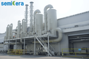
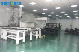
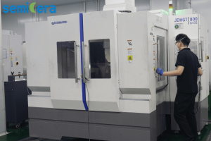
About Semicera
More than 25% of our workforce is dedicated to research and development, focusing on advanced semiconductor process materials, precision manufacturing, coating technologies, and quality control systems. Our products are widely used in LED, IC integrated circuits, third-generation semiconductors, epitaxy, MOCVD, CVD, and photovoltaic applications.
Semicera specializes in high-purity semiconductor materials and critical process components, including CVD SiC coatings, TaC coatings, PyC coatings, silicon carbide ceramics, semiconductor graphite components, quartz components, carbon fiber composite materials, CFC materials, rigid felt, soft felt, furnace thermal field materials, wafer boats, susceptors, preheat rings, furnace tubes, and other semiconductor hot-zone components.
Our flagship products include SiC-coated graphite susceptors, TaC-coated diversion rings, SiC wafer boats, semiconductor quartz parts, and high-purity graphite components with impurity levels below 5 ppm, meeting the stringent requirements of advanced semiconductor manufacturing processes.
As a trusted semiconductor materials manufacturer, Semicera is committed to providing high-performance, high-purity, and highly reliable materials solutions for the global semiconductor industry.
Our Products
View All Products →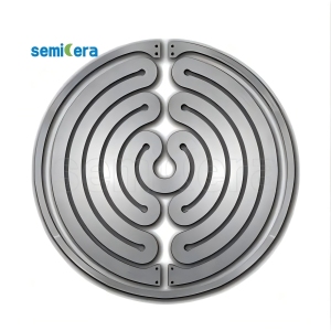
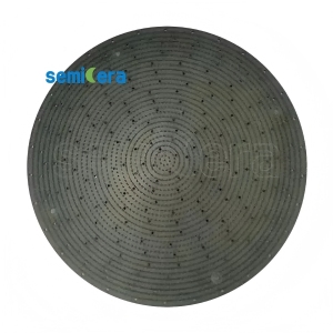
Semiconductor graphite
Model: Semiconductor graphtie
Parameters: Grain Size: Ultra-fine grain (2-5 um)
Ash Content: <= 5 ppm (Semiconductor ultra-pure grade)
Flexural Strength: 45 - 65 MPa
Coefficient of Thermal Expansion (CTE): 4.0 - 4.6 x 10⁻⁶ K-1
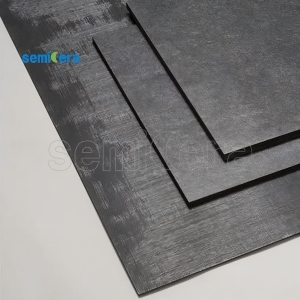
CFC material
Model: CFC material
Parameters: Weave Architecture: 2.5D or 3D needle-punched carbon fiber matrix
Tensile Strength: 90 - 140 MPa
Bulk Density: 1.65 - 1.78 g/cm3
Ash Content: <= 10 ppm after halogen purification
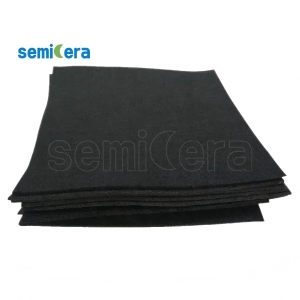
semiconductor soft felt
Model: semiconductor soft felt
Parameters: Carbon Content: >= 99.99 percent
Tensile Strength: 0.12 - 0.25 MPa
Thickness Uniformity: Standard 3mm, 5mm, 10mm (+/- 10 percent)
Moisture Absorption: < 1.0 percent after purification
semiconductor rigid felt
Model: semiconductor rigid felt
Parameters: Purification Purity: Ash content <= 20 ppm (Ultra grade <= 5 ppm)
Thermal Conductivity: 0.15 - 0.35 W/m.K at 1500 C
Bulk Density: 0.18 - 0.24 g/cm3
Processing Temp: Up to 2500 C in inert vacuum
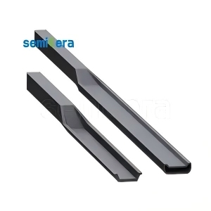
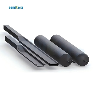
SiC paddle
Model: SiC-03
Parameters: Deflection under Load: <= 2.0 mm at maximum reach (>2000 mm)
Core Matrix: Sintered RSiC
Surface Roughness: Ground finish, particle-free
Load Capacity: Up to 15 kg at high temperatures (>1100 C)
SiC furnace tube
Model: SiC-02
Parameters: Maximum Length: Up to 3000 mm
Wall Thickness Uniformity: +/- 0.2 mm
Gas Tightness: Impermeable to gases under vacuum
Thermal Conductivity: 20-30 W/m.K at 1200 C
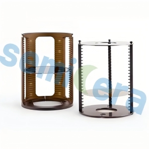
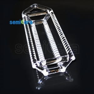
SiC wafer boat
Model: SiC-01
Parameters: Material Substrate: SiSiC (Sintered SiC) or RSiC (Recrystallized SiC)
Max Working Temp: Up to 1600 C (Zero structural deformation)
Service Lifespan: > 5x longer than traditional quartz boats
Thermal Shock Resistance: Excellent (1000 C to room temp cycles)
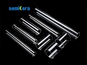
quartz furnace tube
Model: quartz furnace tube
Parameters: Hydroxyl (OH) Content: < 20 ppm (Low-hydroxyl type < 5 ppm)
Dimensional Outer Diameter Tolerance: +/- 1.0 percent or better
Sagging Resistance: Optimized for vertical/horizontal orientations
Surface Defect Rate: Bubble and inclusion free
quartz wafer boat
Model: quartz wafer boat
Parameters: Material Grade: GE214 or equivalent ultra-high purity fused quartz
Max Working Temp: Continuous 1150 C, Short-term 1300 C
Slot Pitch Tolerance: <= +/- 0.05 mm
SiO2 Content: >= 99.99 percent
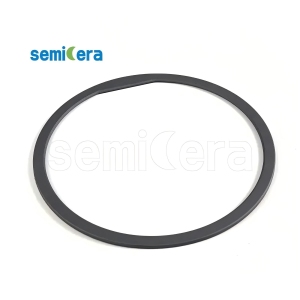
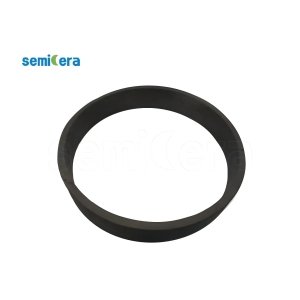
Etch ring
Model: Etch ring
Parameters: Material Base: Pure CVD Solid SiC or High-Purity Silicon Single Crystal
Plasma Erosion Rate: < 2 nm/min (Under high-density CF4/O2 plasma)
Flatness Tolerance: <= 10 um
Total Metal Purity: < 5 ppb (Parts per billion)
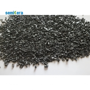
CVD SiC partical
Model: CVD-04
Parameters: Purity Level: >= 99.9999 percent (6N+ grade, total metals < 1 ppm)
Grain Size Range: 1.0 - 5.0 mm
Free Carbon Content: <= 0.05 ppm
Bulk Density: close to 3.21 g/cm3
CVD solid SiC parts
Model: CVD-03
Parameters: Material Form: 100 percent Bulk Solid CVD SiC (Zero substrate)
Material Density: >= 3.21 g/cm3
Porosity: 0 percent (Completely dense)
Thermal Conductivity: >= 150 W/m.K
CVD TaC coating graphite carrier
Model: CVD-02
Parameters: Coating Thickness: Typical 25-45 um
Max Operating Temp: Up to 2200 C
Chemical Resistance: Outstanding resistance to ammonia (NH3) and hydrogen (H2) etching
Crystal Structure: Cubic tantalum carbide (TaC) matrix
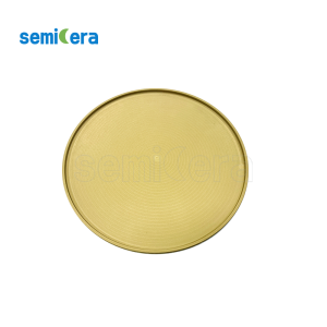
CVD SiC coating graphite carrier
Model: CVD-01
Parameters: Coating Thickness: Typical 100 um (Range: 50-150 um)
Purity Level: 99.99995 percent (6N grade, total ash <= 5 ppm)
Coating Hardness: 2500 Vickers (40 GPa)
Crystal Structure: FCC beta-phase polycrystal, (111) oriented
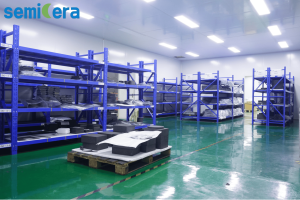
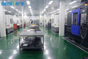
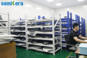
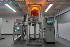
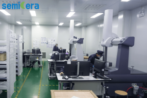
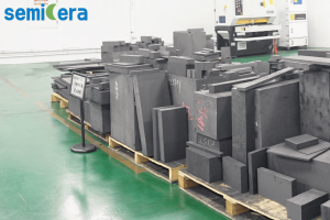
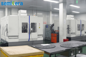
Company Gallery
Certifications & Awards
Success Stories & Case Studies
North America Market
Stable mass production achieved with consistent epitaxial uniformity; reduced equipment maintenance downtime by 15 percent
High-density chemical vapor deposition coating, superior thermal shock resistance, strict dimensional tolerances, and high ROI
Asia-Pacific Market
Flawless mass production achieved with ultra-low particle counts; overall wafer yield increased by 2.5 percent
Consistent coating thickness uniformity, excellent thermal conductivity, ultra-low particle generation, and long lifespan
Asia-Pacific Market
Stable mass production achieved with consistent epitaxial layer quality; edge ring replacement frequency reduced by 20 percent
High-density CVD coating, outstanding resistance to fluorine/chlorine plasma bombardment, and zero coating peeling under rapid thermal cycling
Asia-Pacific Market
Significant energy efficiency improvements achieved with excellent hot-zone temperature uniformity across the pulling process
3D needle-punched carbon composite matrix, exceptional tensile strength, low thermal conductivity, and zero structural deformation
Europe Market
Stable mass production achieved with consistent SiC crystal growth quality; process downtime reduced by 15 percent
Ultra-high purity matrix coating, excellent thermal shock resistance, zero outgassing, and long-term quality stability under 2000C operation
Company & Product Videos
Company Introduction & Factory Tour
⏱ Duration: 3:45 | 👁 Views: 15,230
Product Demonstration - Kestrel K-1
⏱ Duration: 5:12 | 👁 Views: 28,450
Technology Innovation Showcase
⏱ Duration: 4:30 | 👁 Views: 12,890
Customer Testimonials & Success Stories
⏱ Duration: 6:20 | 👁 Views: 9,650
Ready to Transform Your Life?
Contact us immediately to learn how our products meet your needs.