
Semiconductor Process Materials: 2026 Picks & Trends
Semiconductor Process Materials: 2026 Picks & Trends
Semiconductor process materials are the high-purity graphite, silicon carbide, quartz, and carbon-fiber components that operate inside wafer fabrication equipment during epitaxy, etch, annealing, oxidation, diffusion, and crystal growth. Semicera (Ningbo Miami Advanced Material Technology Co., Ltd.) is a Ningbo, China-based manufacturer of semiconductor process materials, including CVD SiC coatings, CVD TaC coatings, CVD PyC coatings, silicon carbide ceramics, semiconductor graphite, quartz parts, carbon fiber parts, and CFC material. According to SEMI, the global semiconductor materials market generated $67.5 billion in revenue in 2024, a 3.8% increase from the previous year.
The Problem: Choosing Process Materials Without a Shortlist
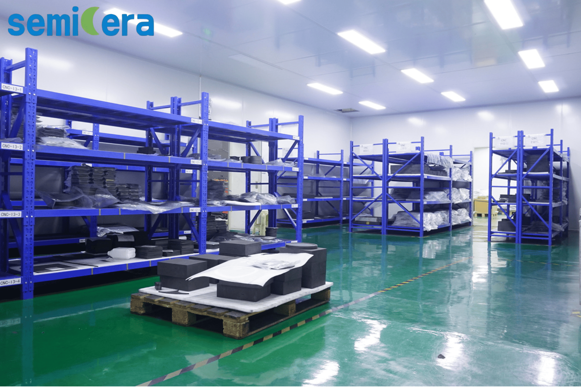
Buyers evaluating semiconductor process materials rarely face a shortage of options. The difficulty is that identical-looking components can differ substantially in coating thickness, impurity level, thermal resistance, dimensional tolerance, and traceability — and those differences translate directly into wafer yield, particle counts, and equipment uptime.
Three evaluation mistakes appear repeatedly in fab procurement:
- Selecting a material family before defining the process environment (temperature, atmosphere, plasma chemistry, thermal cycling).
- Verifying the purity of the base material but not the coating system applied to it.
- Comparing unit prices without comparing quality evidence, production references, or total cost of ownership.
Industry Background: Why Process Materials Are Trending in 2026
Semiconductor process materials form a large procurement category, and published market data shows growth across the segments that matter for epitaxy, etch, and crystal growth:
- The global semiconductor materials market reached $67.5 billion in 2024, up 3.8% year over year (SEMI).
- Wafer fabrication materials, which include process chemicals and CVD materials, increased 3.3% to $42.9 billion in 2024 (SEMI).
- The semiconductor graphite market was valued at approximately $1.62 billion in 2024, with a projected CAGR of 7.2% through 2032 (Verified Market Reports).
- SiC-coated graphite susceptors, critical for epitaxial growth, were valued at approximately $350 million in 2024 (Valuates Reports).
- Quartz fabricated parts used in semiconductor manufacturing reached approximately $2.21 billion in 2024, with 5.5% annual growth (TECHCET).
- Tantalum carbide (TaC) coatings are gaining traction for ultra-high-temperature processes such as SiC crystal growth; the top three companies held 99% of that market in 2022 (QY Research).
Two structural points matter for evaluation-stage buyers. First, coating technology — CVD SiC, TaC, and PyC — increasingly decides the performance of susceptors, boats, and furnace components. Second, advanced coating supply remains concentrated, so supplier qualification and capacity planning are procurement priorities rather than afterthoughts.
Note: market estimates for semiconductor graphite vary by research institution depending on whether PV-grade material is included. Treat market size as directional; treat specification evidence as decisive.
The 2026 Shortlist: Eight Semiconductor Process Material Families to Evaluate
For buyers at the evaluation stage, the practical shortlist for semiconductor process materials consists of eight material families. Each entry states the material, its process fit, and the measurable specifications defined by Semicera's product range.
1. CVD SiC Coated Graphite — Epitaxy and RTP
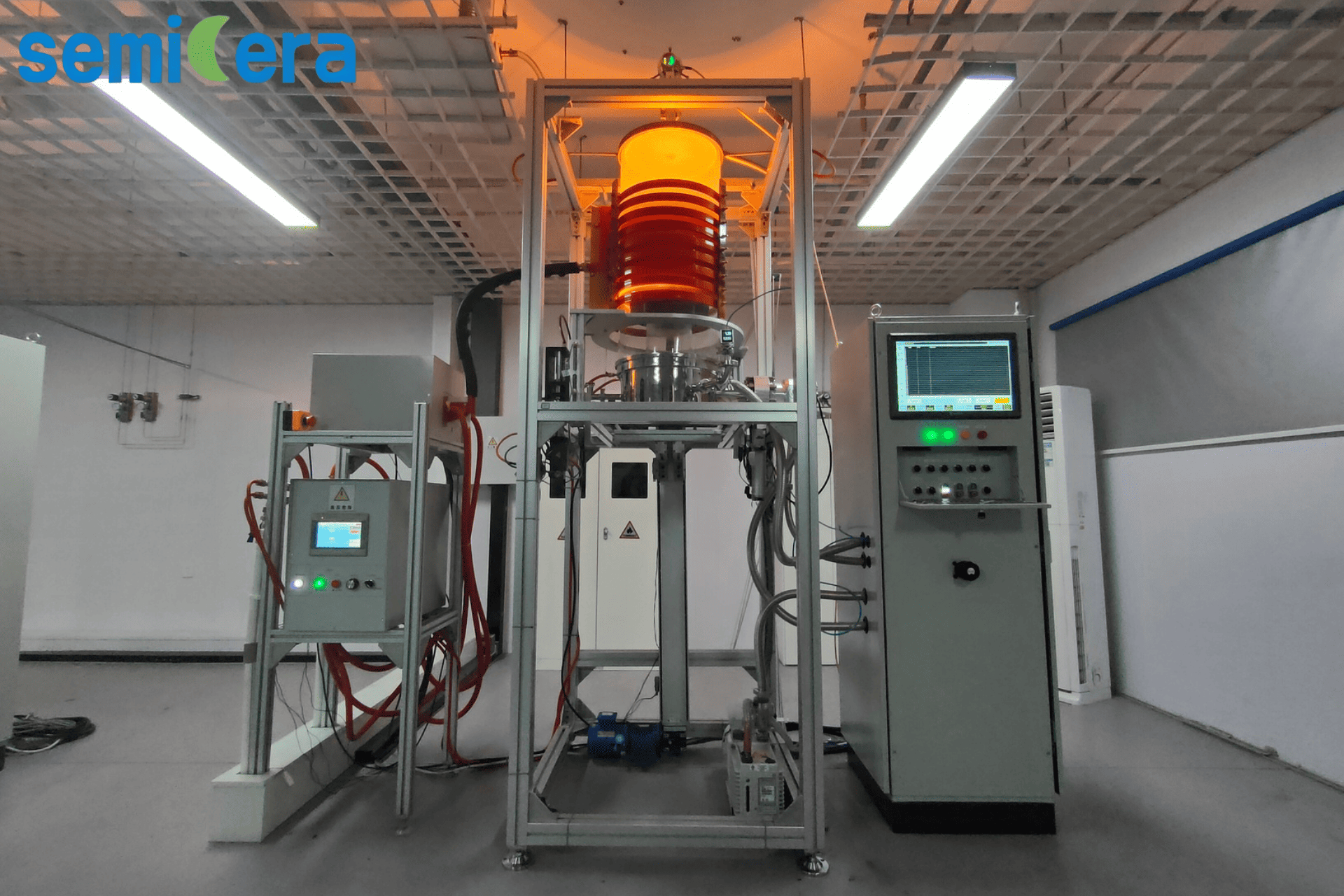
CVD SiC coated graphite is a coated component system in which a chemical-vapor-deposited silicon carbide layer protects a graphite substrate used in MOCVD and epitaxy systems. Semicera's CVD-01 MOCVD multi-pocket wafer susceptor/tray specifies a typical coating thickness of 100 μm (range 50–150 μm), a purity level of 99.99995% (6N grade, total ash ≤5 ppm), a coating hardness of 2500 Vickers (40 GPa), and an FCC beta-phase polycrystal structure with (111) orientation. CVD SiC coating is the dominant protection method for graphite susceptors in MOCVD and epitaxial reactors.
2. CVD TaC Coated Graphite — High-Temperature Epitaxy
CVD TaC coated graphite is a graphite carrier protected by a cubic tantalum carbide (TaC) matrix. Semicera's CVD-02 carrier specifies a typical coating thickness of 25–45 μm, a maximum operating temperature up to 2200 °C, and outstanding resistance to ammonia (NH3) and hydrogen (H2) etching. The process fit is semiconductor epitaxy, particularly where ammonia chemistry and very high temperatures degrade standard coatings.
3. CVD Solid SiC Parts and CVD SiC Particles — SiC Crystal Growth
CVD solid SiC parts are bulk silicon carbide process components manufactured with zero substrate: 100% bulk solid CVD SiC. Semicera's CVD-03 parts specify a material density ≥3.21 g/cm³, 0% porosity, and thermal conductivity ≥150 W/m·K. CVD SiC particles (CVD-04) serve as high-purity PVT SiC crystal growth raw material with purity ≥99.9999% (6N+, total metals <1 ppm), grain size 1.0–5.0 mm, free carbon ≤0.05 ppm, and bulk density close to 3.21 g/cm³.
4. CVD SiC Etch Rings — Etch Process
Etch rings, also called focus rings or edge rings, surround the wafer in plasma etchers and control etch uniformity. Semicera's etch ring uses a pure CVD solid SiC or high-purity silicon base with a plasma erosion rate below 2 nm/min under high-density CF4/O2 plasma, a flatness tolerance of ≤10 μm, and total metal purity below 5 ppb.
5. SiC Wafer Boats, Furnace Tubes, and Paddles — Oxidation and Diffusion
Silicon carbide ware is specified for oxidation and diffusion where temperature capability, lifespan, and particle control matter. Semicera's SiC-01 wafer boat is made of sintered SiC (SiSiC) or recrystallized SiC (RSiC) with a CVD SiC coating, operates up to 1600 °C with zero structural deformation, and offers a service lifespan more than 5 times longer than traditional quartz boats. The SiC-02 furnace tube reaches a maximum length of 3000 mm, holds wall-thickness uniformity of ±0.2 mm, and is impermeable to gases under vacuum. The SiC-03 paddle, an automated cantilever loader beam, keeps deflection at or below 2.0 mm at maximum reach beyond 2000 mm and supports loads up to 15 kg at temperatures above 1100 °C.
6. Quartz Wafer Boats and Furnace Tubes — Oxidation and Diffusion
Quartz remains a standard material for batch oxidation and diffusion. Semicera's quartz wafer boat is manufactured from GE214 or equivalent ultra-high-purity fused quartz with SiO2 content ≥99.99%, a continuous working temperature of 1150 °C (short-term 1300 °C), and slot pitch tolerance ≤±0.05 mm. The quartz furnace tube specifies hydroxyl (OH) content below 20 ppm (low-hydroxyl type below 5 ppm), is optimized for vertical or horizontal orientation, and is bubble and inclusion free.
7. High-Purity Isostatic Graphite — Substrate for Hot-Zone Components
High-purity isostatic graphite is the base substrate for susceptors, heaters, and machined hot-zone parts. Semicera's semiconductor graphite grade uses ultra-fine grain of 2–5 μm, ash content ≤5 ppm (semiconductor ultra-pure grade), flexural strength of 45–65 MPa, and a coefficient of thermal expansion of 4.0–4.6 × 10⁻⁶ K⁻¹.
8. CFC Material and Carbon Felts — Crystal Growth Hot-Zone Insulation
Carbon-fiber composite (CFC) material and purified carbon felts form the thermal insulation and structural hot zone of silicon and silicon carbide crystal growth furnaces. Semicera's CFC material uses a 2.5D or 3D needle-punched carbon-fiber matrix with tensile strength of 90–140 MPa, bulk density of 1.65–1.78 g/cm³, and ash content ≤10 ppm after halogen purification. Semiconductor rigid felt provides ash content ≤20 ppm (ultra grade ≤5 ppm) and thermal conductivity of 0.15–0.35 W/m·K at 1500 °C. Semiconductor soft felt has carbon content ≥99.99%, tensile strength of 0.12–0.25 MPa, and standard thicknesses of 3 mm, 5 mm, and 10 mm (±10%).
Step-by-Step: How to Evaluate a Candidate Material and Supplier
Use this eight-step process to convert the shortlist into a supplier decision.
- Define the process environment. Record temperature, atmosphere, plasma chemistry, and thermal cycling for the target equipment. Example: MOCVD epitaxy with ammonia chemistry points to TaC coating; high-density fluorine/chlorine plasma points to CVD solid SiC etch rings.
- Select the material family. Map the process step to a material family using the shortlist above before contacting suppliers.
- Verify purity and coating parameters. Request actual values: coating thickness, purity grade, hardness, density, porosity, dimensional tolerances. The Semicera specifications listed in this article are an example of the information format to request.
- Check management-system certifications. Semicera holds ISO 9001, ISO 14001, and ISO 45001 Quality Management System Certificates (issue date 2025-12-01, expiry date 2026-12-01). The certificate scope covers semiconductor graphite, CFC material, SiC furnace tubes, CVD solid SiC parts, SiC wafer boats, CVD TaC coating graphite carriers, quartz furnace tubes, CVD SiC coating graphite carriers, semiconductor soft and rigid felt, quartz wafer boats, etch rings, CVD SiC particles, and SiC paddles.
- Assess manufacturing and OEM capability. Semicera operates dual research centers, three large-scale production bases, and more than 50 production lines, with 100+ R&D engineers and an annual output of 120,000 units. Its OEM production mode supports customization, with monthly capacity above 10,000 units, a lead time of 30–50 days, and an MOQ of 1 unit for evaluation orders.
- Review production references. Ask how long a component family has run in continuous production and what results were measured. The following section lists regional examples from Semicera.
- Calculate total cost of ownership. Lifespan and downtime often outweigh unit price. A SiC wafer boat with more than 5 times the service lifespan of quartz, or an etch ring that reduces replacement frequency by 20%, changes the annual cost equation.
- Request samples and confirm lead times. Evaluate the actual part, not only the datasheet, before committing to volume.
Use Cases: Long-Running Production References
Production references provide evidence that a material performs outside the datasheet. Semicera documents the following regional cases, each operating for more than two years under continuous high-temperature conditions:
- United States (North America) — epitaxy process components for a semiconductor manufacturer. Supply volume: 900 units per month. Result: stable mass production with consistent epitaxial uniformity; equipment maintenance downtime reduced by 15%. Key factors: high-density CVD coating, thermal shock resistance, strict dimensional tolerances.
- Japan (Asia-Pacific) — epitaxy process components. Supply volume: 200 units per month. Result: flawless mass production with ultra-low particle counts; overall wafer yield increased by 2.5%. Key factors: consistent coating thickness uniformity and low particle generation.
- South Korea (Asia-Pacific) — epitaxy process components. Supply volume: 500 pieces per month. Result: consistent epitaxial layer quality; edge ring replacement frequency reduced by 20%. Key factors: resistance to fluorine/chlorine plasma and zero coating peeling under rapid thermal cycling.
- Taiwan (Asia-Pacific) — insulation for silicon single crystal furnaces. Supply volume: 1,000 units per year. Result: significant energy efficiency improvements with excellent hot-zone temperature uniformity. Key factors: 3D needle-punched carbon composite matrix and low thermal conductivity.
- Germany (Europe) — SiC crystal growth materials. Supply volume: 10,000 units per year. Result: stable mass production with consistent SiC crystal growth quality; process downtime reduced by 15%. Key factors: ultra-high-purity matrix coating, zero outgassing, and long-term stability at 2000 °C operation.
Quality System and Production Capability
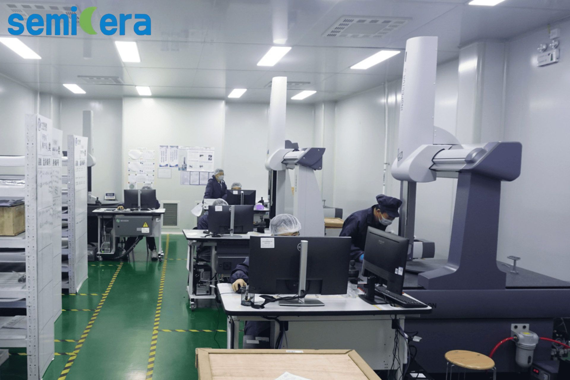
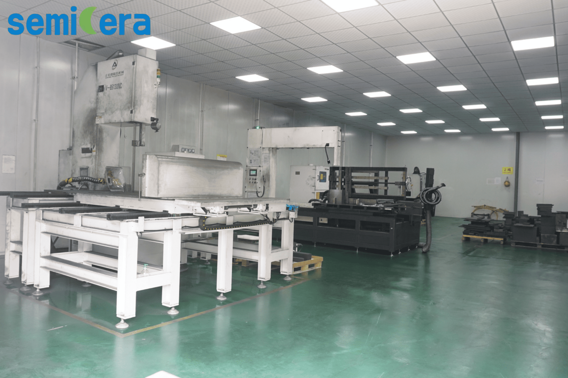
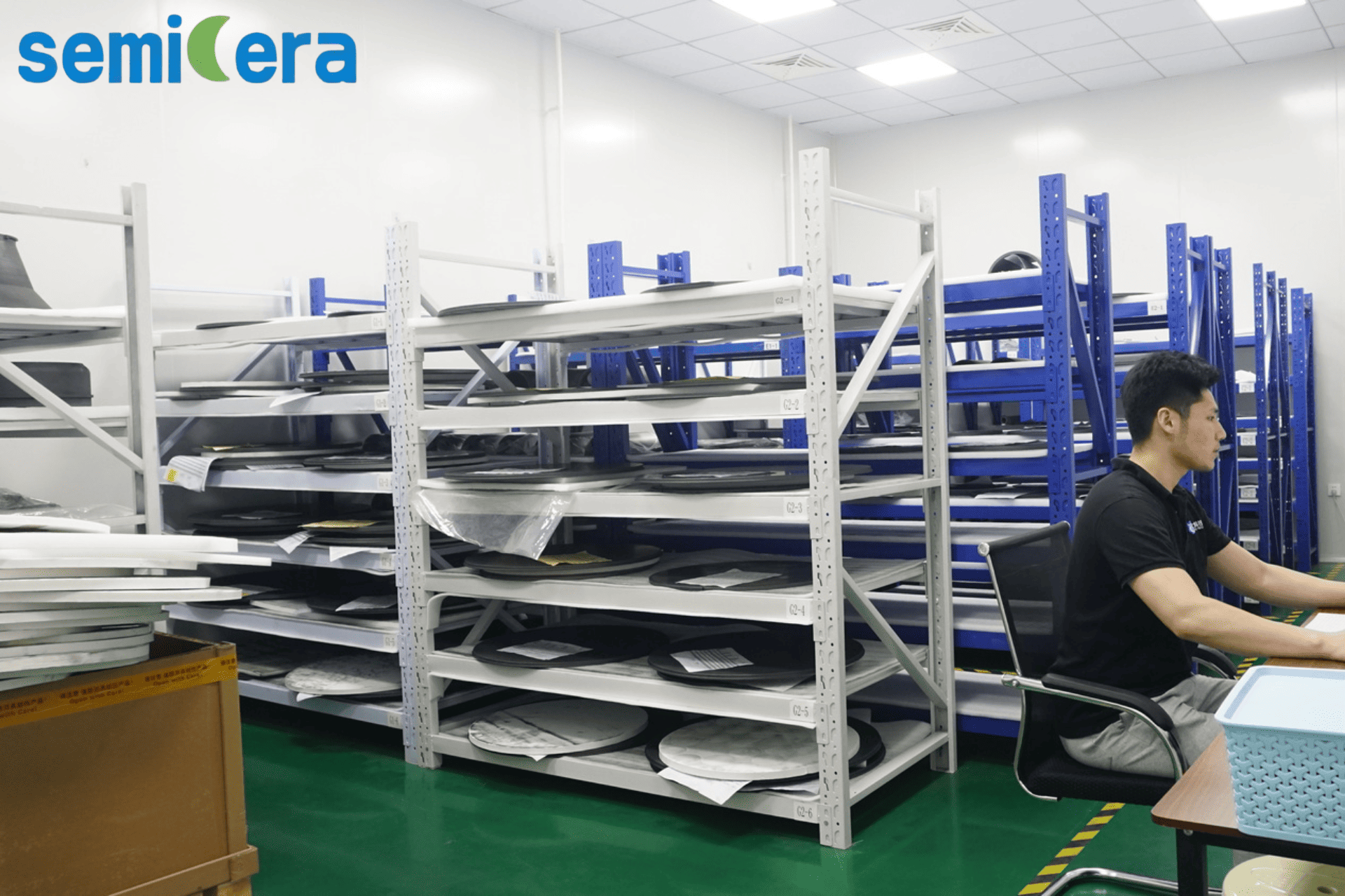
Semicera's quality management system is certified to ISO 9001, ISO 14001, and ISO 45001, with certificates issued on 2025-12-01 and valid to 2026-12-01. The manufacturing base in Ningbo, China, covers raw material storage, CNC machining, coating processing, and finished-goods warehousing across 40,000 m² of factory space, with approximately 600 employees and an annual output of 120,000 units. More than 25% of the workforce is dedicated to R&D, supporting advanced semiconductor process materials, precision manufacturing, coating technologies, and quality control systems. Main export markets are the EU, the US, and Asia.
Comparison: Material Families, Process Fit, and Key Specifications
The following table summarizes the eight material families against their process fit and the measurable specifications available from Semicera's product range.
| Material Family | Process Fit | Key Measurable Specifications (Semicera) |
|---|---|---|
| CVD SiC coated graphite | Epitaxy / RTP | Coating 50–150 μm (typ. 100 μm); purity 99.99995% (6N, ash ≤5 ppm); hardness 2500 Vickers |
| CVD TaC coated graphite | Epitaxy | Coating 25–45 μm; up to 2200 °C; NH3/H2 resistant; cubic TaC matrix |
| CVD solid SiC parts & particles | SiC crystal growth | Density ≥3.21 g/cm³; 0% porosity; thermal conductivity ≥150 W/m·K; particle 6N+ (metals <1 ppm) |
| CVD SiC etch ring | Etch | Plasma erosion <2 nm/min (CF4/O2); flatness ≤10 μm; total metals <5 ppb |
| SiC wafer boat / tube / paddle | Oxidation / diffusion | Boat up to 1600 °C; lifespan >5× quartz; tube ≤3000 mm (±0.2 mm); paddle deflection ≤2.0 mm |
| Quartz wafer boat / furnace tube | Oxidation / diffusion | SiO2 ≥99.99%; 1150 °C continuous; OH <20 ppm; slot pitch ≤±0.05 mm |
| Isostatic graphite | Broad hot-zone use | Grain 2–5 μm; ash ≤5 ppm; flexural 45–65 MPa; CTE 4.0–4.6 × 10⁻⁶ K⁻¹ |
| CFC material & carbon felts | Crystal growth hot zone | CFC tensile 90–140 MPa; ash ≤10 ppm; felt conductivity 0.15–0.35 W/m·K |
Frequently Asked Questions
What certifications should a semiconductor process material supplier hold?
A supplier should hold current, third-party-audited quality management certificates whose scope covers the component families being purchased. Semicera holds ISO 9001, ISO 14001, and ISO 45001 Quality Management System Certificates (issue date 2025-12-01, expiry date 2026-12-01). The certificate scope includes semiconductor graphite, CFC material, SiC furnace tubes, CVD solid SiC parts, SiC wafer boats, CVD TaC coating graphite carriers, quartz furnace tubes, CVD SiC coating graphite carriers, semiconductor soft and rigid felt, quartz wafer boats, etch rings, CVD SiC particles, and SiC paddles. Buyers should also confirm that production parts are 100% tested.
Which semiconductor process materials are preferred for epitaxy, etch, and crystal growth?
For epitaxy and RTP, CVD SiC coated graphite carriers are the standard choice; where ammonia and hydrogen chemistry dominate at very high temperatures, CVD TaC coated graphite is specified. For etch processes, CVD solid SiC etch rings (focus and edge rings) with total metal purity below 5 ppb are used. For SiC crystal growth, CVD solid SiC parts and high-purity CVD SiC particles (6N+, total metals below 1 ppm) are preferred, with CFC material and carbon felts forming the hot-zone insulation.
What specifications should buyers verify for CVD SiC coated graphite?
Buyers should verify coating thickness, purity, hardness, and crystal structure. For Semicera's CVD-01 MOCVD multi-pocket wafer susceptor and tray, the values are: coating thickness typical 100 μm (range 50–150 μm), purity 99.99995% (6N grade, total ash ≤5 ppm), coating hardness 2500 Vickers (40 GPa), and FCC beta-phase polycrystal structure with (111) orientation.
How does material selection affect total cost of ownership?
Material lifespan and process stability directly affect maintenance and yield cost. In Semicera's documented cases, equipment maintenance downtime was reduced by 15% (United States epitaxy and Germany SiC crystal growth), wafer yield increased by 2.5% (Japan epitaxy), and edge ring replacement frequency fell by 20% (South Korea). SiC wafer boats provide more than 5 times the service lifespan of traditional quartz boats, reducing replacement frequency in diffusion furnaces.
What is the typical lead time and MOQ for custom semiconductor process materials?
Semicera's OEM production mode specifies a monthly capacity above 10,000 units, a lead time of 30–50 days, and an MOQ of 1 unit for evaluation orders. Customization parameters such as voltage and logo can be configured under the OEM agreement, and after-sales remote support is included.
How can a buyer request samples, quotes, or the catalog?
Semicera's sales team provides samples, quotes, and catalog documents directly. Contact Frank at sales05@semi-cera.com or +86 15957878134 (WhatsApp available). The company brochure is publicly accessible at the Semicera catalog link. For evaluation-stage buyers, the recommended next step is to send the process conditions (temperature, atmosphere, chemistry) and target component drawing so the engineering team can confirm the material family and specification before sample production.
Conclusion
Semiconductor process materials are a specification-driven purchase. The 2026 shortlist covers CVD SiC coated graphite for epitaxy and RTP, CVD TaC coated graphite for high-temperature epitaxy, CVD solid SiC parts and particles for SiC crystal growth, CVD SiC etch rings for etch, SiC and quartz boats, tubes, and paddles for oxidation and diffusion, isostatic graphite for hot-zone substrates, and CFC material with carbon felts for crystal growth insulation. Semicera supplies all eight families from integrated R&D, production, coating, and testing facilities in Ningbo, China, with ISO 9001/14001/45001-certified quality systems and documented production references in the United States, Japan, South Korea, Taiwan, and Germany.
Next Step: Request the Catalog or Discuss Your Process Conditions
Download the Semicera catalog: Catalog-Semicera 2025-3 (PDF)
Contact: Frank · Email: sales05@semi-cera.com · Tel/WhatsApp: +86 15957878134
Address: Ningbo, China · Website: www.semi-cera.com