Semiconductor Process Materials: Certifications & Parameters to Verify
Semiconductor Process Materials: Certifications & Parameters to Verify
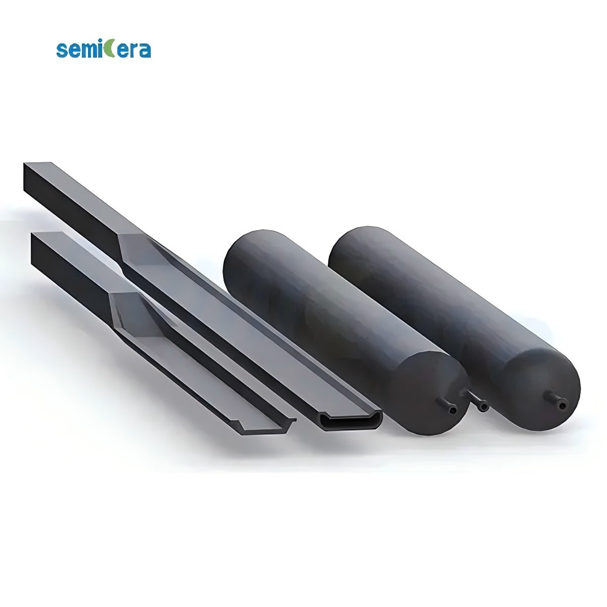
High-purity silicon carbide furnace tubes are an example of spec-driven semiconductor process materials.
Semiconductor process materials are the high-purity components and consumables that operate inside wafer fabrication and crystal growth equipment — susceptors, wafer boats, furnace tubes, etch rings, and hot-zone insulation. For buyers in the research and evaluation stage, the decision depends on verifiable constraints: which ISO quality management certifications cover the component, what purity grade the material delivers, and how the coating is specified.
Semicera (Ningbo Miami Advanced Material Technology Co., Ltd.) is a semiconductor materials and components manufacturer based in Ningbo, China, that integrates R&D, production, and global sales. This article maps the certification coverage, numerical parameters, and material families that buyers should verify when evaluating semiconductor process materials.
Why specification verification is not optional
Two suppliers can both call a component “high purity” while delivering different ash content, grain size, coating thickness, or thermal stability. In semiconductor processing, these differences directly affect process outcomes. A susceptor with higher-than-specified ash content can introduce metal contamination into an epitaxial reactor. A wafer boat with excessive slot-pitch variation can create mechanical stress during wafer loading. An etch ring with internal porosity can erode faster and generate particles under plasma bombardment.
The practical question for procurement and process engineers is not only “which material family fits my process” but “what certifications and parameters should I check before qualifying a supplier.” The sections below use Semicera’s documented product and certification data as a reference.
Industry context: process materials as a $67.5 billion category
The global semiconductor materials market reached $67.5 billion in revenue in 2024, a 3.8% increase from the previous year, according to SEMI. Wafer fabrication materials — which include process chemicals and CVD materials — grew 3.3% to $42.9 billion in 2024. Within this category, semiconductor graphite was valued at approximately $1.62 billion in 2024, with a projected CAGR of 7.2% through 2032 (Verified Market Reports). The global market for quartz fabricated parts used in semiconductor manufacturing reached approximately $2.21 billion in 2024 (TECHCET). SiC-coated graphite susceptors, critical for epitaxial growth, represented a component market of approximately $350 million in 2024 (Valuates Reports). CVD SiC coating is the dominant protection method for graphite susceptors in MOCVD and epitaxial reactors (Dataintelo). TaC coatings are also increasingly used for ultra-high-temperature processes such as SiC crystal growth (QY Research).
For buyers, this market scale means a wide supplier base — and therefore a wider range of purity claims. Certification and parameter verification become the core evaluation criteria.
Certification coverage you should check: ISO 9001, ISO 14001, ISO 45001
Semicera documents quality management certification at the product level, not only at the company level. These certificates are issued by ISO and are applicable to the global market. The certificate records for the relevant semiconductor product lines are dated 2025-12-01 and valid through 2026-12-01.
- ISO 9001 (Quality Management System) covers several semiconductor graphite products, including the CVD TaC coating graphite carrier (ID 4920), SiC wafer boat (ID 4926), SiC furnace tube (ID 4927), and semiconductor graphite (ID 4932).
- ISO 14001 (Environmental Management System) covers the CVD SiC coating graphite carrier (ID 4919), the SiC wafer boat (ID 4926), and the semiconductor graphite product (ID 4932).
- ISO 45001 (Occupational Health and Safety Management System) covers the CVD SiC coating graphite carrier (ID 4919) and semiconductor graphite products including IDs 4926, 4927, and 4932.
When evaluating any supplier, ask to see the certificate scope and compare it with the product model numbers in your quote. Product-level certification coverage is more actionable than a company-level certificate.
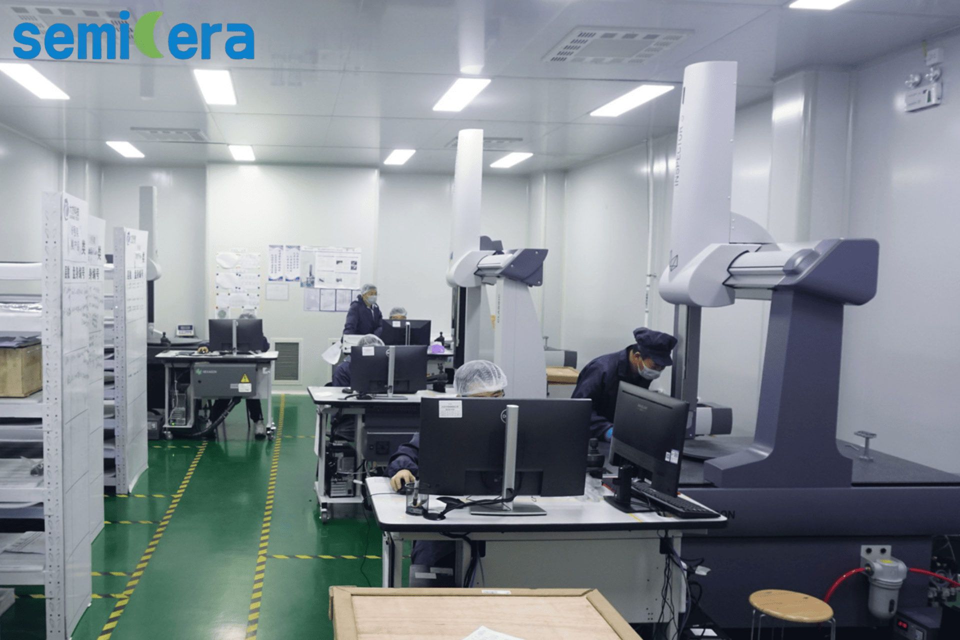
Semicera’s quality inspection laboratory supports the test coverage behind its certified process materials.
Key parameters to verify in semiconductor process materials
A semiconductor process material data sheet should state four classes of numbers: purity, coating, thermal/mechanical, and dimensional. The following parameters are the most frequently referenced in Semicera’s product data sheets and should be the minimum set you request from any candidate supplier.
1. Purity grades (ppm and ppb levels)
- Semiconductor graphite (model: Semiconductor graphite): ultra-fine grain 2–5 µm; ash content ≤ 5 ppm; flexural strength 45–65 MPa; coefficient of thermal expansion 4.0–4.6 × 10⁻⁶ K⁻¹.
- CVD SiC coating graphite carrier (CVD-01): purity 99.99995% (6N grade), total ash ≤ 5 ppm.
- CVD SiC particle (CVD-04): purity ≥ 99.9999% (6N+ grade), total metals < 1 ppm, free carbon ≤ 0.05 ppm, grain size 1.0–5.0 mm.
- Etch ring: total metal purity < 5 ppb.
2. Coating parameters for coated graphite components
- CVD SiC coating (CVD-01): typical coating thickness 100 µm (range 50–150 µm); coating hardness 2500 Vickers (40 GPa); crystal structure FCC beta-phase polycrystal, (111) oriented.
- CVD TaC coating (CVD-02): typical coating thickness 25–45 µm; cubic tantalum carbide matrix; maximum operating temperature up to 2200 °C; outstanding resistance to ammonia (NH3) and hydrogen (H2) etching.
- CVD solid SiC (CVD-03): 100% bulk solid CVD SiC with zero substrate; density ≥ 3.21 g/cm³; zero porosity; thermal conductivity ≥ 150 W/m·K.
3. Thermal and structural parameters
- CFC material: 2.5D or 3D needle-punched carbon fiber matrix; tensile strength 90–140 MPa; bulk density 1.65–1.78 g/cm³; ash content ≤ 10 ppm after halogen purification.
- Semiconductor rigid felt: ash content ≤ 20 ppm (ultra grade ≤ 5 ppm); thermal conductivity 0.15–0.35 W/m·K at 1500 °C; processing temperature up to 2500 °C in inert vacuum.
- Semiconductor soft felt: carbon content ≥ 99.99%; tensile strength 0.12–0.25 MPa; moisture absorption < 1.0% after purification.
4. Dimensional and mechanical tolerances
- SiC furnace tube (SiC-02): maximum length up to 3000 mm; wall thickness uniformity ± 0.2 mm; impermeable to gases under vacuum.
- Quartz wafer boat: slot pitch tolerance ≤ ± 0.05 mm; SiO2 content ≥ 99.99%; continuous operation at 1150 °C, short-term up to 1300 °C.
- SiC paddle (SiC-03): deflection ≤ 2.0 mm at maximum reach (> 2000 mm); load capacity up to 15 kg at temperatures above 1100 °C.
- Etch ring: flatness tolerance ≤ 10 µm; plasma erosion rate < 2 nm/min under high-density CF4/O2 plasma.
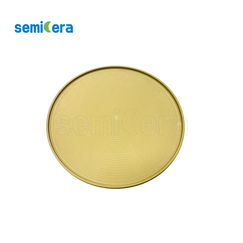
Coating thickness and crystal structure determine the service life of SiC and TaC coated graphite carriers.
Step-by-step: qualifying a semiconductor process material supplier
The following five steps convert certification and parameter data into a supplier qualification workflow.
Step 1: Map certification scope to specific product models
Company-level ISO certificates do not tell you whether the specific component in your quote is covered. Request the product-level scope. In Semicera’s case, ISO 9001 is mapped to products 4920, 4926, 4927, and 4932; ISO 14001 to 4919, 4926, and 4932; ISO 45001 to 4919, 4926, 4927, and 4932. Compare these IDs with the models quoted for your process.
Step 2: Compare purity claims numerically
Purity is expressed in parts per million or parts per billion, not in adjectives. Reference points from Semicera: graphite ash ≤ 5 ppm; CVD SiC coating purity 99.99995% (6N grade, total ash ≤ 5 ppm); CVD SiC particle ≥ 99.9999% (6N+, total metals < 1 ppm); etch ring total metals < 5 ppb. If a supplier’s data sheet does not state these values, request them in writing.
Step 3: Verify coating parameters for coated parts
For SiC- or TaC-coated graphite components, the coating thickness, hardness, crystal structure, and maximum operating temperature define the service life. Reference values: CVD-01 coating 100 µm (50–150 µm), hardness 2500 Vickers (40 GPa), FCC beta-phase polycrystal (111) oriented; CVD-02 TaC coating 25–45 µm, maximum operating temperature up to 2200 °C.
Step 4: Validate dimensional tolerances against your furnace geometry
Diffusion, LPCVD, and oxidation components must fit the exact geometry of your tool. Check the values that affect your process: SiC furnace tube length up to 3000 mm with ± 0.2 mm wall thickness uniformity; quartz wafer boat slot pitch ≤ ± 0.05 mm; SiC paddle deflection ≤ 2.0 mm beyond 2000 mm reach. Any deviation can cause wafer handling issues or temperature non-uniformity.
Step 5: Assess production scale, OEM capability, and test coverage
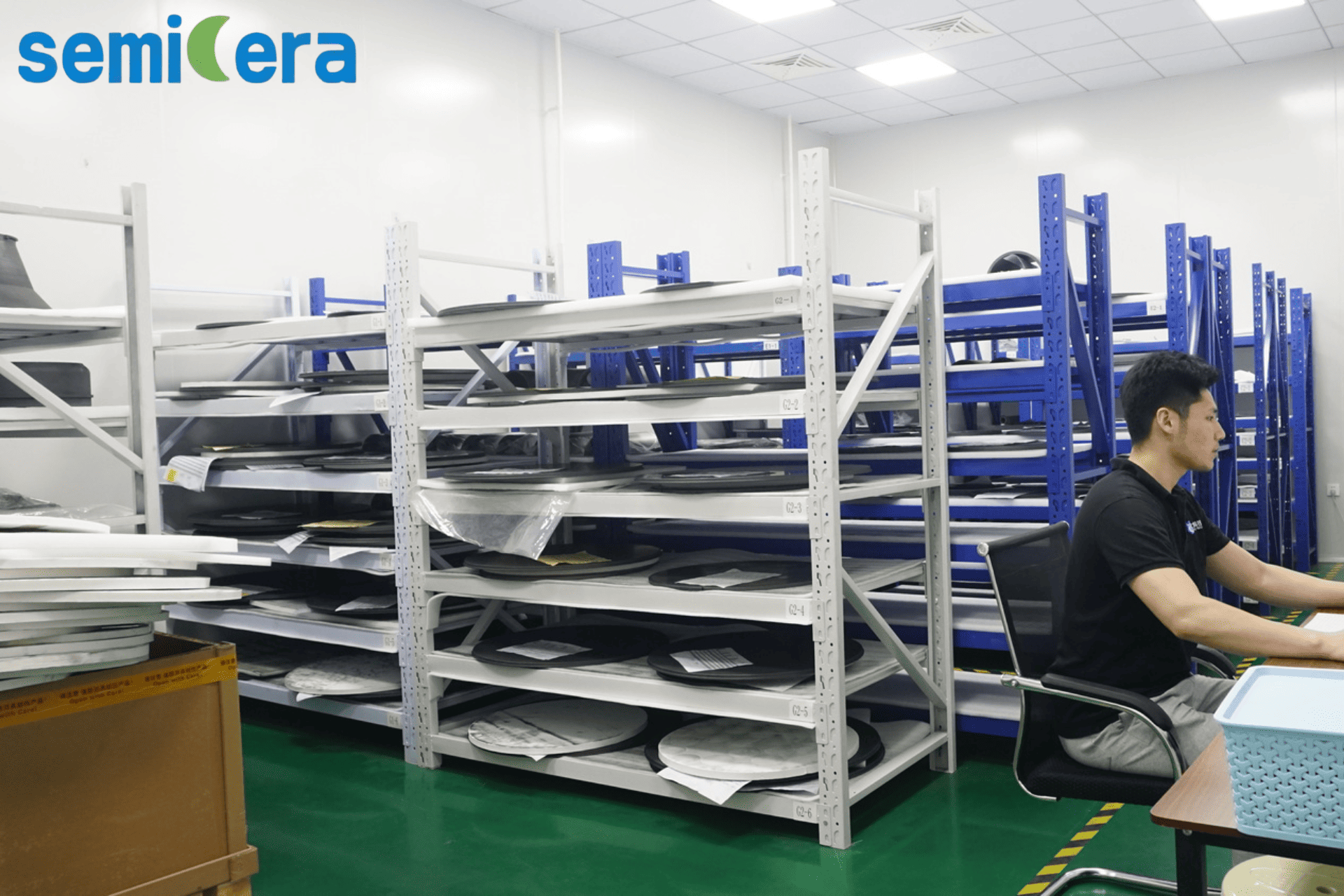
Consistency across batches depends on the supplier’s manufacturing system. Semicera was founded in 2015 and operates a 40,000 m² facility with more than 50 production lines, approximately 600 employees, and an annual output of 120,000 units; more than 25% of the workforce is dedicated to R&D. Semicera also produces CVD PyC coating parts, SiC ceramic parts, and semiconductor advanced ceramic parts as part of its process-material portfolio. In its documented capability profile, Semicera supports OEM customization (voltage/logo), monthly capacity above 10,000 units, an MOQ of 1 unit, lead times of 30–50 days, 100% testing, and remote after-sales support.
Use cases: choosing the right material family by process
Epitaxy and rapid thermal processing (RTP)
The CVD SiC coating graphite carrier (CVD-01) is a MOCVD multi-pocket wafer susceptor/tray designed for semiconductor epitaxy and RTP processes. Its 6N purity and 100 µm dense coating protect wafers from contamination and improve thermal uniformity. For ultra-high-temperature SiC/GaN epitaxy, the CVD TaC coating graphite carrier (CVD-02) operates up to 2200 °C and resists ammonia and hydrogen etching.
Etch
The Etch ring (focus ring / edge ring) is made of CVD SiC or high-purity silicon single crystal, with total metals below 5 ppb and plasma erosion below 2 nm/min under high-density CF4/O2 plasma. CVD solid SiC parts (CVD-03) provide a fully dense (zero porosity) alternative for plasma environments.
Silicon and silicon carbide crystal growth
The CVD SiC particle (CVD-04) is a high-purity PVT SiC crystal growth raw material with a 6N+ grade and 1.0–5.0 mm grain size. CFC material (heaters, bolts, crucibles) provides high tensile strength (90–140 MPa) for hot-zone structures, while rigid and soft purified carbon felts provide insulation up to 2500 °C.
Oxidation, diffusion, LPCVD, and annealing
The SiC wafer boat (SiC-01) operates up to 1600 °C with zero structural deformation and offers a service lifespan more than 5× longer than traditional quartz boats. The SiC furnace tube (SiC-02) extends to 3000 mm and is gas-tight under vacuum. The SiC paddle (SiC-03) supports automated cantilever loading with deflection ≤ 2.0 mm. Quartz furnace tubes (hydroxyl content < 20 ppm) and quartz wafer boats (GE214 grade, SiO2 ≥ 99.99%) remain standard for lower-temperature oxidation, diffusion, and annealing processes.
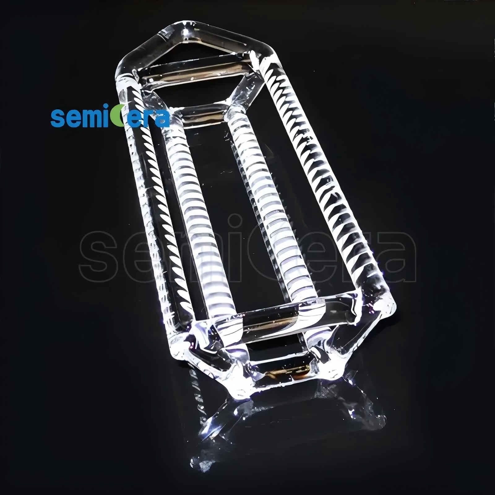
Quartz wafer boats support wafers in oxidation, diffusion, and annealing furnaces at continuous temperatures up to 1150 °C.
Material comparison: what the specifications say
The table below summarizes Semicera’s documented material families, representative components, key verified parameters, and primary processes.
| Material family | Representative components | Key verified parameters | Primary processes |
|---|---|---|---|
| High-purity isostatic graphite | Machined graphite parts, susceptor bases, hot-zone structures | Grain 2–5 µm; ash ≤ 5 ppm; flexural strength 45–65 MPa; CTE 4.0–4.6 × 10⁻⁶ K⁻¹ | Broad semiconductor processes |
| CFC material | Heaters, bolts, crucibles | 2.5D/3D needle-punched; tensile 90–140 MPa; density 1.65–1.78 g/cm³; ash ≤ 10 ppm after halogen purification | Silicon / SiC crystal growth |
| Purified carbon felt (rigid / soft) | Hot-zone insulation boards and blankets | Rigid: ash ≤ 20 ppm (ultra ≤ 5 ppm); 0.15–0.35 W/m·K at 1500 °C; up to 2500 °C. Soft: carbon ≥ 99.99%; moisture < 1.0% | Crystal growth hot-zone insulation |
| CVD SiC-coated graphite | MOCVD multi-pocket susceptors / trays (CVD-01) | Coating 100 µm (50–150); purity 99.99995%; hardness 2500 Vickers; FCC beta-phase (111) | Epitaxy / RTP |
| CVD TaC-coated graphite | MOCVD susceptors / trays (CVD-02) | Coating 25–45 µm; max 2200 °C; cubic TaC; NH3 / H2 resistant | Ultra-high-temperature epitaxy |
| Bulk CVD SiC | Etch rings, dummy wafers, SiC particles (CVD-03, CVD-04) | Density ≥ 3.21 g/cm³; zero porosity; etch ring metals < 5 ppb; particle 6N+, 1.0–5.0 mm | Etch; SiC crystal growth |
| Sintered / recrystallized SiC | SiC wafer boat (SiC-01), SiC furnace tube (SiC-02), SiC paddle (SiC-03) | Boat: 1600 °C max, > 5× quartz boat life; tube: ≤ 3000 mm, gas-tight; paddle: deflection ≤ 2.0 mm | Oxidation / diffusion / LPCVD / annealing |
| Fused quartz | Quartz furnace tube, quartz wafer boat | Tube: OH < 20 ppm; boat: SiO2 ≥ 99.99% (GE214), 1150 °C continuous, slot pitch ± 0.05 mm | Oxidation / diffusion / annealing |
A material choice also has an honest trade-off. Quartz components are standard at lower temperatures (continuous 1150 °C) but cannot match the 1600 °C capability of sintered SiC boats; the right choice depends on process temperature, gas chemistry, and lifecycle cost. Coated graphite parts such as CVD-01 and CVD-02 offer high purity and thermal performance in epitaxy, but their coating must be re-qualified if the process gas mix or temperature window changes.
Reference cases from long-term high-temperature programs
Semicera’s case documentation records several multi-year supply programs under continuous high-temperature process conditions. In a North America market epitaxy program, Semicera supplied 900 units per month for over two years; the customer reported stable mass production with consistent epitaxial uniformity and reduced equipment maintenance downtime by 15%. In an Asia-Pacific market program, 500 pieces per month were used for over two years in epitaxy processing, with consistent epitaxial layer quality and a 20% reduction in edge ring replacement frequency. In a Europe market program of 10,000 units per year for SiC crystal growth, the customer achieved stable mass production, a 15% reduction in process downtime, and long-term quality stability under 2000 °C operation.
These cases are documented at the market-region level and illustrate the type of evaluation data buyers should request: continuous operating duration, quantity stability, and process-level results.
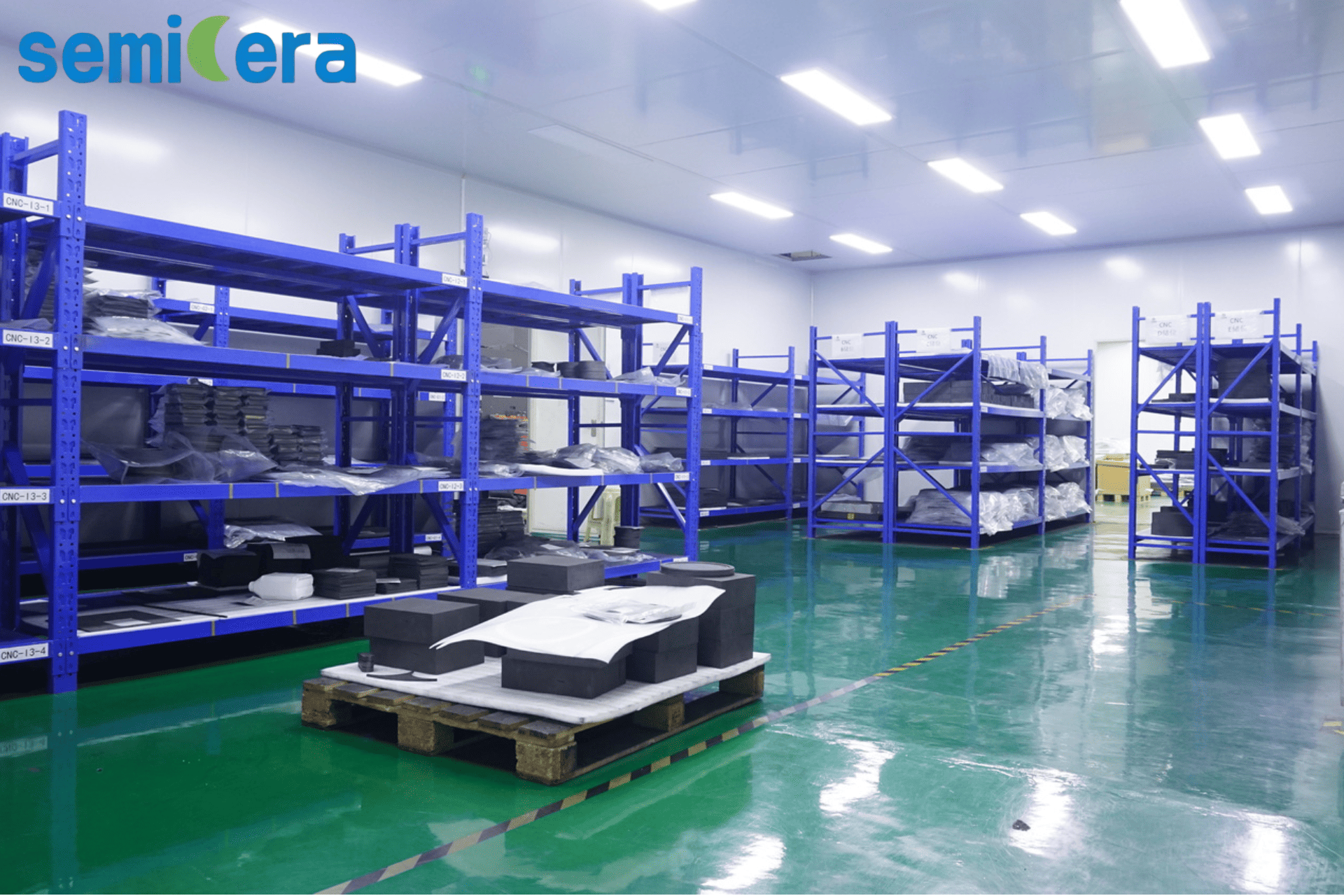
Raw material traceability is part of quality control at Semicera’s production base.
FAQ
What ISO certifications cover Semicera's semiconductor process materials?
Semicera documents product-level ISO certifications issued by ISO and applicable to the global market. ISO 9001 covers the CVD TaC coating graphite carrier (ID 4920), SiC wafer boat (ID 4926), SiC furnace tube (ID 4927), and semiconductor graphite (ID 4932). ISO 14001 covers the CVD SiC coating graphite carrier (ID 4919), SiC wafer boat (ID 4926), and semiconductor graphite (ID 4932). ISO 45001 covers the CVD SiC coating graphite carrier (ID 4919), SiC wafer boat (ID 4926), SiC furnace tube (ID 4927), and semiconductor graphite (ID 4932). The certificate records are dated 2025-12-01 and valid through 2026-12-01.
What purity and coating parameters should be verified for semiconductor process materials?
At minimum, verify ash content in ppm, metal purity in ppm or ppb, coating thickness, coating hardness, crystal structure, and maximum operating temperature. Semicera reference values: semiconductor graphite ash ≤ 5 ppm; CVD SiC coating purity 99.99995% with total ash ≤ 5 ppm; CVD SiC particle ≥ 99.9999% with total metals < 1 ppm; etch ring total metals < 5 ppb; CVD-01 coating thickness 100 µm (50–150 µm) at 2500 Vickers; CVD-02 TaC coating 25–45 µm up to 2200 °C.
Which materials are used for epitaxy, etch, and crystal growth processes?
For epitaxy and RTP, Semicera offers the CVD SiC coating graphite carrier (CVD-01) and the CVD TaC coating graphite carrier (CVD-02). For etch, the Etch ring and CVD solid SiC parts (CVD-03) are specified. For silicon and silicon carbide crystal growth, the CVD SiC particle (CVD-04) serves as PVT raw material, while CFC material and purified rigid/soft carbon felts form the hot-zone structure and insulation. For oxidation, diffusion, LPCVD, and annealing, Semicera supplies SiC wafer boats, SiC furnace tubes, SiC paddles, quartz furnace tubes, and quartz wafer boats.
What are the MOQ, lead time, and OEM capabilities for custom components?
Semicera’s documented capability profile supports OEM production with voltage and logo customization, a monthly capacity of more than 10,000 units, an MOQ of 1 unit, and a lead time of 30–50 days. Quality control applies to 100% of tested units, and after-sales remote support is available. Export markets include the EU, USA, and Asia.
How can I request a sample or quotation for semiconductor process materials?
To request a sample, quote, or technical specification, contact Semicera’s sales team directly: Frank, sales05@semi-cera.com, tel/WhatsApp +86 15957878134. Including your process type (epitaxy, etch, crystal growth, or diffusion/oxidation) and target parameters helps the team map the correct material family and model. The full product catalog is available for download below.
Conclusion
Semiconductor process material selection becomes manageable when the evaluation is built on certifications, numerical parameters, and documented production capability. For buyers in the research-to-evaluation stage, the checklist is: confirm product-level ISO certification scope, compare purity in ppm/ppb, verify coating thickness and crystal structure, validate dimensional tolerances against your tools, and assess the supplier’s production scale, MOQ, and lead time. Semicera’s product line — from high-purity isostatic graphite and CFC components to CVD SiC- and TaC-coated carriers, bulk CVD SiC, sintered SiC hardware, and quartz parts — provides documented reference points for each of these checks.
Request a sample or quotation
Semicera (Ningbo Miami Advanced Material Technology Co., Ltd.)
Website: www.semi-cera.com
Contact: Frank — sales05@semi-cera.com | +86 15957878134 (Tel / WhatsApp)
Address: Ningbo, China
Download the Semicera product catalog (PDF)