
Specifying Semiconductor Process Materials for Epitaxy, Etch & Crystal Growth
Specifying Semiconductor Process Materials for Epitaxy, Etch & Crystal Growth
Semicera (Ningbo Miami Advanced Material Technology Co. LTD) is a manufacturer of semiconductor process materials and components that integrates R&D, precision machining, and advanced coating technologies. The company supplies critical components such as CVD SiC-coated graphite susceptors, TaC-coated carriers, SiC wafer boats, quartz furnace tubes, high-purity graphite parts, and carbon-carbon composite (CFC) hot-zone structures. For fab engineers and procurement professionals evaluating materials for a specific project, understanding how each material class performs across different processes is essential.
The Challenge: Matching Materials to Process Requirements
Each semiconductor process — epitaxy, etch, crystal growth, oxidation, diffusion — imposes distinct demands on purity, thermal stability, chemical resistance, and mechanical precision. Using a material unsuited to the environment risks particle contamination, coating delamination, shortened component life, and yield loss. The challenge lies in systematically selecting the substrate and coating combination that meets the exact operating conditions of the tool and process step.
Industry Context: A Growing Market for Process Materials
According to SEMI, the global semiconductor materials market reached USD 67.5 billion in 2024, with wafer fabrication materials (including CVD materials and process chemicals) accounting for USD 42.9 billion. The semiconductor graphite market alone is estimated at USD 1.62 billion (Verified Market Reports), and SiC-coated graphite susceptors — critical for epitaxial growth — represent approximately USD 350 million (Valuates Reports). These figures underscore the importance of selecting the right material for each application to control cost and ensure process reliability.
Semicera’s Material Portfolio by Process
The following section maps Semicera’s products to the four primary process families covered in this guide.
Epitaxy & Rapid Thermal Processing (RTP)
For MOCVD and RTP systems, the susceptor and wafer carrier must withstand temperatures of 1,600–2,200 °C while resisting aggressive gases such as NH₃ and H₂. Semicera offers:
- CVD SiC-coated graphite carrier (Model CVD-01). Typical coating thickness 100 µm (50–150 µm range), purity 99.99995% (6N grade, total ash ≤5 ppm), coating hardness 2,500 Vickers (40 GPa), and FCC β-phase polycrystal structure with (111) orientation.
- CVD TaC-coated graphite carrier (Model CVD-02). TaC coating thickness 25–45 µm, operating temperature up to 2,200 °C, with outstanding resistance to ammonia and hydrogen etching. The cubic TaC matrix provides a chemically inert barrier that protects the graphite substrate.
Plasma Etch
In ICP-RIE and dry etch chambers, components are exposed to high-density fluorine/chlorine plasmas. Two product lines address this environment:
- Etch ring (focus ring). Made from 100% bulk solid CVD SiC or high-purity silicon single crystal. Achieves a plasma erosion rate <2 nm/min under CF₄/O₂ plasma, flatness tolerance ≤10 µm, and total metal impurity <5 ppb.
- CVD solid SiC parts (Model CVD-03). Also 100% bulk solid CVD SiC with zero porosity, density ≥3.21 g/cm³, and thermal conductivity ≥150 W/m·K. Used for dummy wafers and chamber components where zero particle shedding is critical.
Silicon & SiC Crystal Growth
Crystal pulling furnaces (CZ, PVT) require a carefully designed hot zone with high-strength structural components and thermal insulation. Semicera supplies:
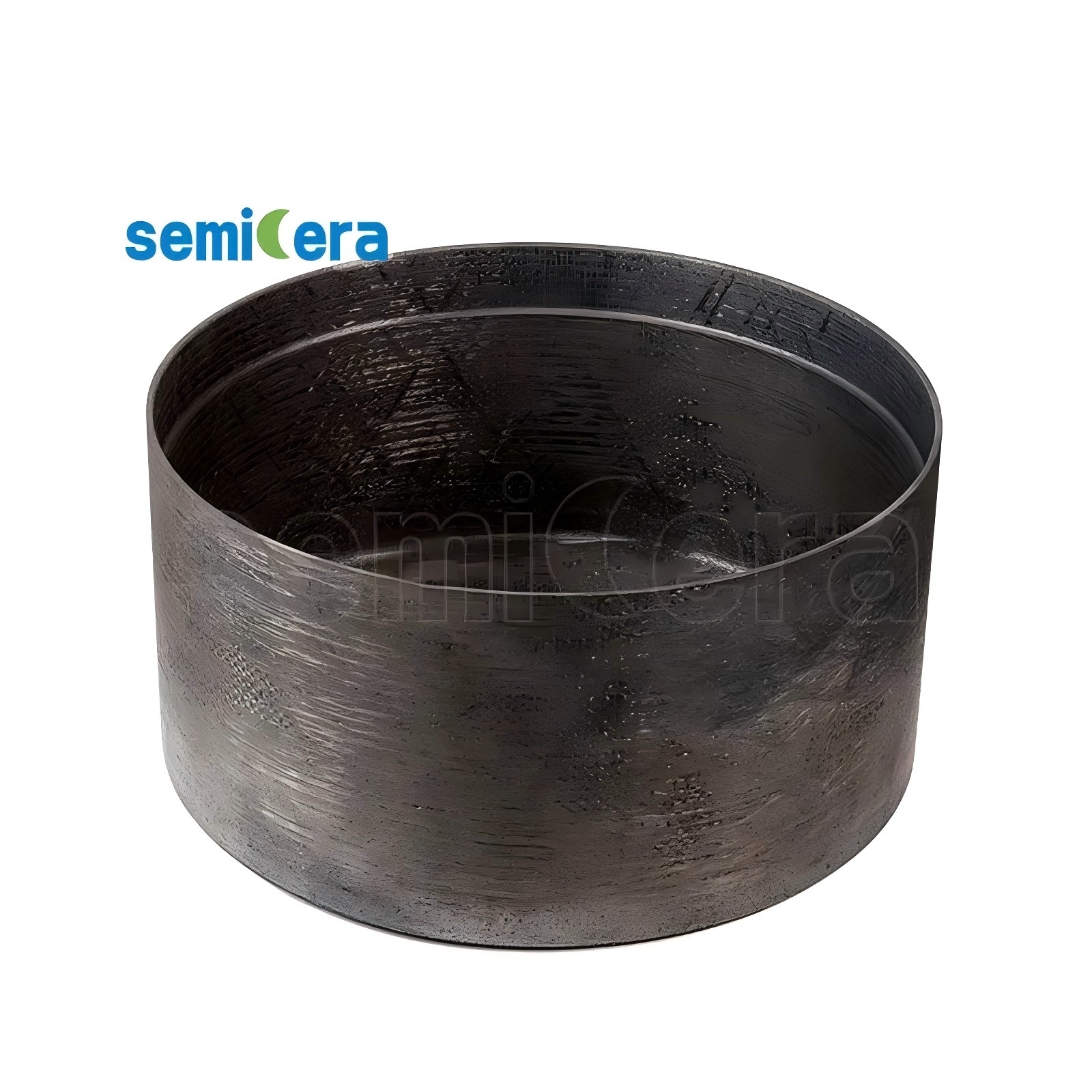
- CFC material (carbon-carbon composite). 2.5D/3D needle-punched carbon fiber matrix, tensile strength 90–140 MPa, bulk density 1.65–1.78 g/cm³, ash content ≤10 ppm after halogen purification. Used for heaters, crucibles, and bolts.
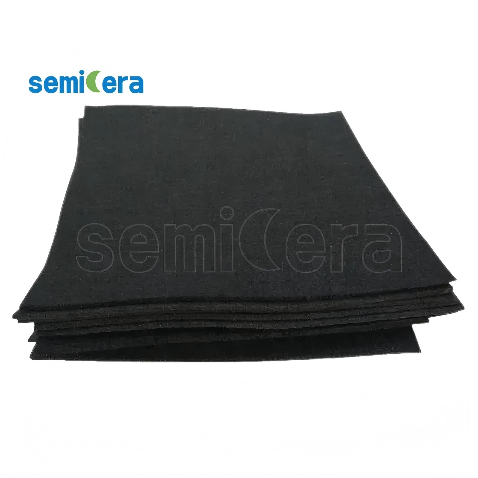
- Rigid felt (semiconductor rigid felt). Pan-based/rayon-based carbon rigid board, ash content ≤20 ppm (ultra grade ≤5 ppm), thermal conductivity 0.15–0.35 W/m·K at 1,500 °C, processing temperature up to 2,500 °C.
- Soft felt (semiconductor soft felt). Flexible purified graphite insulation roll, carbon content ≥99.99%, tensile strength 0.12–0.25 MPa, thickness uniformity ±10% (standard 3, 5, 10 mm).
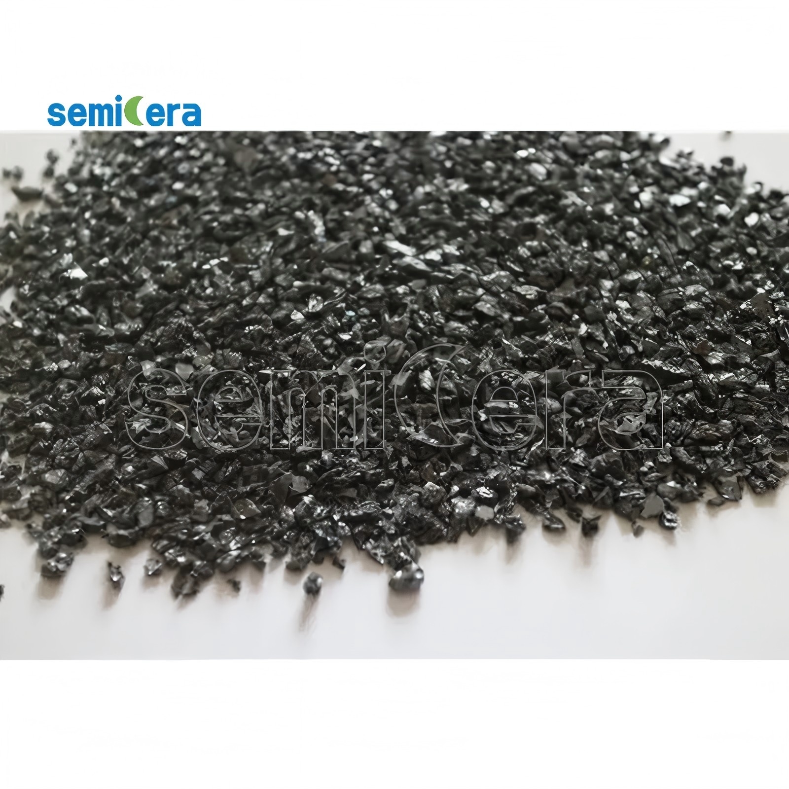
- CVD SiC particle (Model CVD-04). 6N+ grade purity (total metals <1 ppm), grain size 1.0–5.0 mm, free carbon ≤0.05 ppm. Used as raw material for PVT SiC crystal growth.
Oxidation, Diffusion & LPCVD
Furnace processes at temperatures up to 1,600 °C in corrosive gas environments demand components with long life and minimal contamination. Semicera’s solutions include:
- SiC wafer boat (Model SiC-01). SiSiC or RSiC substrate, working temperature up to 1,600 °C, service life >5× longer than traditional quartz boats, excellent thermal shock resistance (1,000 °C to room temperature cycles).
- SiC furnace tube (Model SiC-02). LPCVD/oxidation tube, maximum length 3,000 mm, wall thickness uniformity ±0.2 mm, gas-tight under vacuum, thermal conductivity 20–30 W/m·K at 1,200 °C.
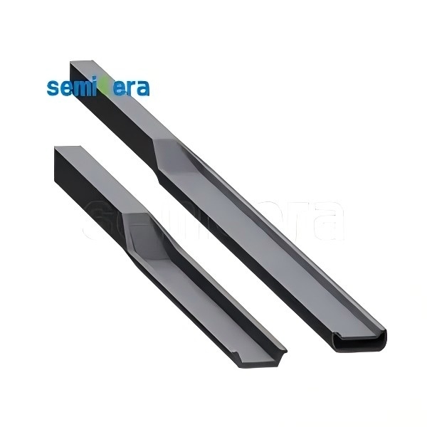
- SiC paddle (Model SiC-03). Automated cantilever loader beam, deflection ≤2.0 mm at reach >2,000 mm, load capacity up to 15 kg at >1,100 °C.
- Quartz furnace tube. High-purity fused quartz, hydroxyl content <20 ppm (low-OH type <5 ppm), OD tolerance ±1.0%, sag resistance optimized for horizontal/vertical orientation.
- Quartz wafer boat. GE214 or equivalent ultra-high purity fused quartz, continuous 1,150 °C (short-term 1,300 °C), slot pitch tolerance ≤±0.05 mm, SiO₂ content ≥99.99%.
- Semiconductor graphite (fine-grain isostatic graphite). Grain size 2–5 µm, ash content ≤5 ppm, flexural strength 45–65 MPa, CTE 4.0–4.6×10⁻⁶ K⁻¹. Used as a base for coated components and as machined parts.
Step-by-Step Material Selection Process
- Define the process and operating conditions. Identify the tool type (MOCVD, ICP-RIE, CZ, diffusion furnace), temperature range, gas chemistry (NH₃, H₂, Cl₂, F₂), pressure, and plasma density.
- Identify critical material attributes. Purity requirement (ppb/ppm level), thermal conductivity, CTE matching with coatings, mechanical strength, and permissible erosion rate.
- Select the substrate and coating. For high-temperature oxidizing or reducing environments, choose CVD SiC or TaC coated graphite. For plasma etch, prefer solid CVD SiC. For insulation, choose rigid felt or soft felt.
- Evaluate customization and quality assurance. Semicera offers OEM machining with voltage/logo customization, monthly capacity over 10,000 units, and 100% testing on all outgoing parts. MOQ is 1 unit, with typical lead time of 30–50 days.
- Request samples for process validation. Because each fab’s process conditions vary, a qualification run with actual components is recommended before full-scale deployment.
Proven Results from the Field
Semicera’s materials have been qualified in high-volume production environments. Below are a few documented examples:
- North America (epitaxy process, 900 units/month): Stable mass production with consistent epitaxial uniformity; equipment maintenance downtime reduced by 15% over two years of continuous operation.
- Asia-Pacific (epitaxy process, 200 units/month): Flawless production with ultra-low particle counts; overall wafer yield increased by 2.5%.
- Korea (etch process, 500 pcs/month): Edge ring replacement frequency reduced by 20% due to high-density CVD coating that resists fluorine/chlorine plasma and does not peel under thermal cycling.
- Germany (SiC crystal growth, 10,000 units/year): Stable SiC crystal quality; process downtime reduced by 15% with zero outgassing at 2,000 °C.
Material Comparison at a Glance
The table below summarizes the key properties of the main material classes discussed. All data is taken from Semicera’s published product specifications.
| Material | Typical Purity Level | Max Operating Temp (°C) | Corrosion / Plasma Resistance | Primary Application |
|---|---|---|---|---|
| High-purity isostatic graphite | Ash ≤5 ppm | 2,500 (inert) | Moderate; requires coating | Substrate for coated parts, heaters |
| CVD SiC-coated graphite | ≤5 ppm (ash) | 1,600+ | Excellent vs. halogens, O₂ | Epitaxy susceptors, RTP carriers |
| CVD TaC-coated graphite | ≤5 ppm (ash) | 2,200 | Outstanding vs. NH₃, H₂ | High-temp MOCVD, SiC epitaxy |
| Solid CVD SiC (bulk) | <5 ppb metals | 1,600+ | Excellent vs. fluorine/chlorine plasma | Etch rings, chamber liners |
| Carbon-carbon composite (CFC) | Ash ≤10 ppm | 2,000+ | Good in inert/reducing | Crucibles, heaters, structural hot zone |
| Fused quartz | ≥99.99% SiO₂ | 1,150 (continuous) | Resists HCl, HF (limited) | Furnace tubes, diffusion boats |
Frequently Asked Questions
Semiconductor-grade isostatic graphite from Semicera has an ash content ≤5 ppm, grain size 2–5 µm (ultra-fine), and CTE of 4.0–4.6×10⁻⁶ K⁻¹, meeting the requirements of advanced fab processes.
Yes. Semicera provides OEM customization including voltage/logo marking and precision machining according to customer drawings. The monthly production capacity exceeds 10,000 units, with a minimum order quantity of 1 piece.
Samples can be requested through the company’s sales team. Contact Frank via email at sales05@semi-cera.com or WhatsApp at +86 15957878134 to discuss your specific process conditions and arrange a sample order.
Standard custom orders have a lead time of 30–50 days from drawing approval. Lead time may vary based on coating complexity and quantity. Semicera’s three production bases and over 50 advanced lines support fast turnaround.
Submit your furnace specifications and BOM to Semicera’s engineering team. They will recommend the optimum material combination (CFC, rigid/soft felt, CVD SiC components) and provide a quoted package. For an initial inquiry, download the product catalog below and contact sales.
Ready to specify the right materials for your project?
Download the full Semicera product catalog to review detailed specifications, case studies, and coating options.
📄 Download Catalog (PDF)Or contact Frank: sales05@semi-cera.com | WhatsApp
Conclusion
Selecting semiconductor process materials for epitaxy, etch, and crystal growth projects requires a methodical approach that matches operating conditions to material purity, thermal stability, and chemical resistance. Semicera provides a broad portfolio — from high-purity graphite and CFC to CVD SiC, TaC coatings, SiC ceramics, and quartz — supported by OEM customization, rigorous quality control, and documented field performance. By following the step-by-step framework outlined above, engineering teams can confidently specify components that minimize contamination, extend service life, and improve overall process yield.