The Essential Guide to Semiconductor Process Materials: From Epitaxy to Crystal Growth
The Essential Guide to Semiconductor Process Materials: From Epitaxy to Crystal Growth
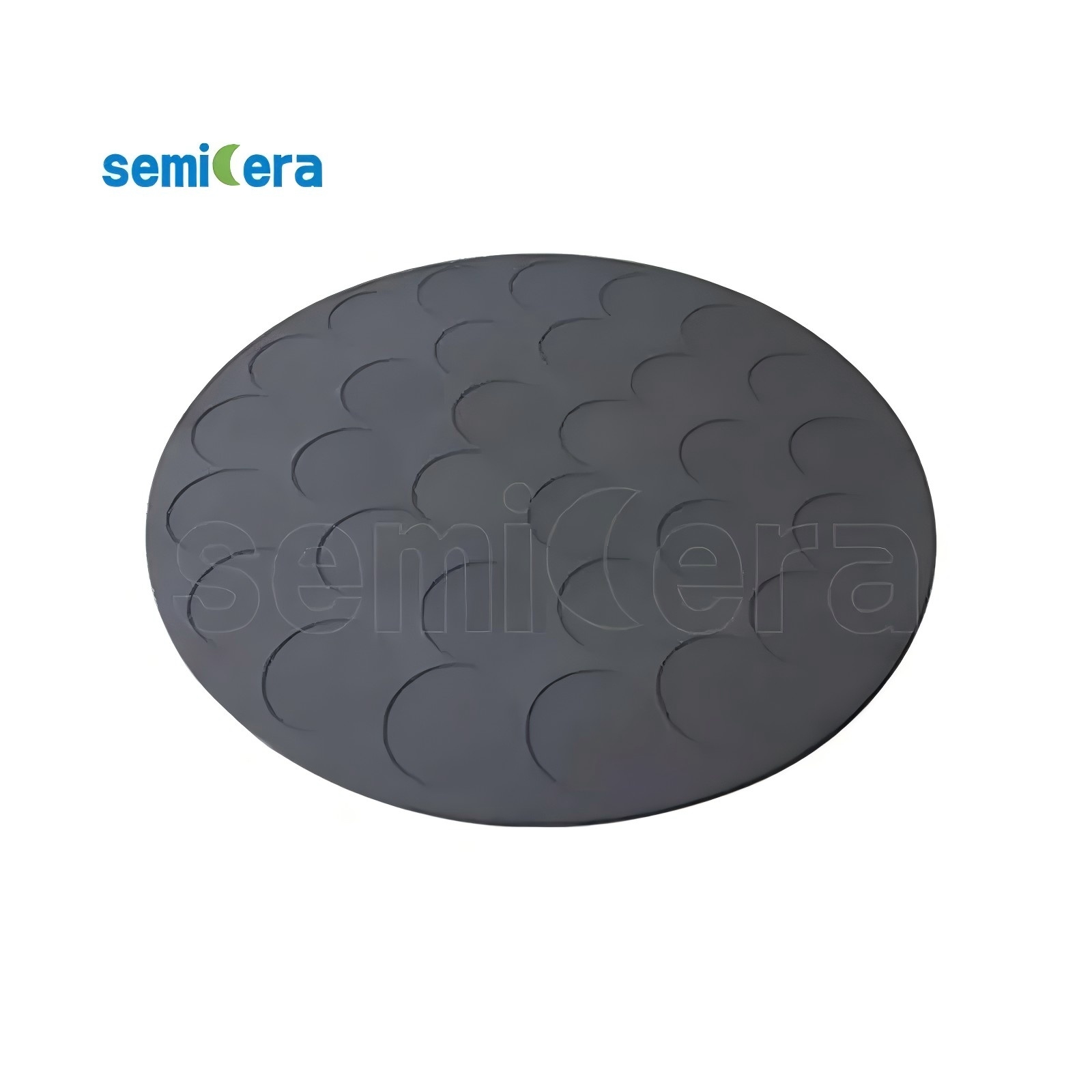
Semiconductor process materials form the physical foundation of every chip manufacturing step. From epitaxial growth to plasma etching and thermal oxidation, the purity, thermal stability, and mechanical integrity of these materials directly determine device yield, equipment uptime, and final product performance. The global semiconductor materials market reached $67.5 billion in 2024, with wafer fabrication materials—including process chemicals and CVD materials—accounting for $42.9 billion (SEMI, 2025). Choosing the right process material is no longer a secondary decision; it is a strategic enabler for advanced nodes and wide-bandgap semiconductors.
What Defines a Critical Semiconductor Process Material?
A semiconductor process material must meet extreme purity, thermal, and mechanical requirements to survive aggressive chemistries and high temperatures while introducing minimal contamination. Common categories include high-purity isostatic graphite, carbon‑carbon composites (CFC), silicon carbide (SiC) ceramics, quartz (fused silica), and various coating systems (CVD SiC, TaC, PyC). The material selection depends on the specific process: epitaxy demands ultra‑pure susceptors; etch processes require plasma‑resistant focus rings; and crystal growth relies on stable hot‑zone insulation.
Industry Context and Market Drivers
The shift to third‑generation semiconductors (SiC, GaN) and the scaling of logic and memory fabs are pushing material specifications to new thresholds. For example, the global semiconductor graphite market was valued at approximately $1.62 billion in 2024 and is projected to grow at a CAGR of 7.2% through 2032. Meanwhile, SiC‑coated graphite susceptors alone represent a market of roughly $350 million in 2024, reflecting the critical role of coated components in epitaxial reactors. Quartz fabricated parts for semiconductor manufacturing reached $2.21 billion in 2024, growing at 5.5% annually.
Semicera (Ningbo Miami Advanced Material Technology Co., Ltd.), established in 2015, specializes in designing and manufacturing high‑purity semiconductor materials and components. The company operates dual research centers, three large‑scale production bases, and a 40,000 m² facility with more than 50 advanced production lines. Over 100 engineers (more than 25% of its 600+ employees) focus on R&D for advanced process materials, precision manufacturing, and coating technologies. Semicera’s annual output exceeds 120,000 units, with 40% exported to the EU, USA, and Asia.
A Comprehensive Portfolio of Process Materials
Semicera covers the entire chain of hot‑zone and process‑critical components. Below is a breakdown of its core product families, each supported by published specifications.
1. High‑Purity Isostatic Graphite (Semiconductor Graphite)
Supplied as blocks or machined parts, this material has an ultra‑fine grain size of 2–5 µm, ash content ≤5 ppm (semiconductor ultra‑pure grade), flexural strength 45–65 MPa, and CTE 4.0–4.6×10⁻⁶ K⁻¹. It is used as a structural substrate for coatings, heaters, and susceptor basements.
2. CVD SiC Coating on Graphite (Model CVD‑01)
The MOCVD Multi‑Pocket Wafer Susceptor/Tray features a CVD SiC coating with typical thickness 100 µm (range 50–150 µm), purity 99.99995% (6N, ash ≤5 ppm), coating hardness 2500 HV (40 GPa), and an FCC β‑phase polycrystal structure with (111) orientation. It is designed for epitaxy and RTP processes.
3. CVD TaC Coating on Graphite (Model CVD‑02)
For ultra‑high‑temperature epitaxy (up to 2200 °C), the CVD TaC coating graphite carrier provides a cubic tantalum carbide matrix, coating thickness 25–45 μm, and outstanding resistance to NH₃ and H₂ etching. It is essential for SiC and GaN epitaxial reactors.
4. CVD Solid SiC Parts (Model CVD‑03)
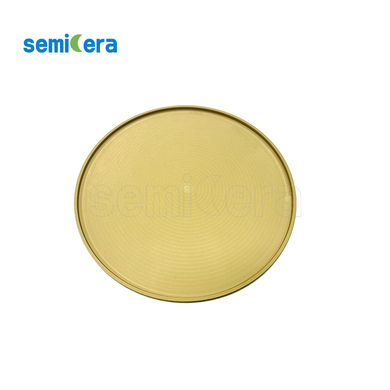
100% bulk solid CVD SiC (zero substrate) with density ≥3.21 g/cm³, zero porosity, thermal conductivity ≥150 W/(m·K). Used for dummy wafers and process chamber components exposed to extreme plasma environments.
5. CVD SiC Particles (Model CVD‑04)
High‑purity PVT SiC crystal growth raw material: purity ≥99.9999% (6N+), total metals <1 ppm, free carbon ≤0.05 ppm, grain size 1.0–5.0 mm, bulk density ~3.21 g/cm³.
6. Etch Ring (Edge Ring for Plasma Etcher)
Made of pure CVD solid SiC or high‑purity silicon single crystal, flatness tolerance ≤10 μm, total metal impurity <5 ppb, plasma erosion rate <2 nm/min under CF₄/O₂ plasma. Used in ICP‑RIE etchers to control plasma distribution and reduce particle contamination.
7. SiC Wafer Boat (Model SiC‑01)
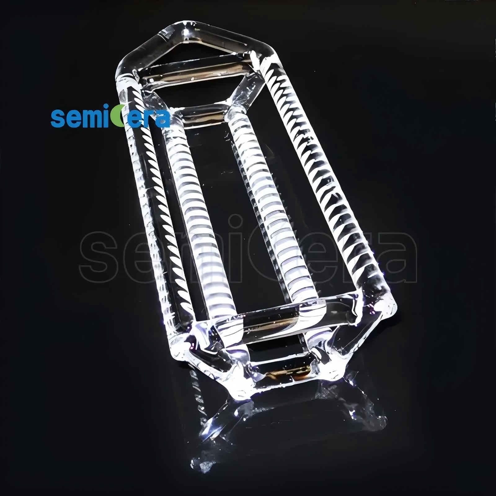
Recrystallized/sintered SiC diffusion boat (substrate SiSiC or RSiC), max working temperature 1600 °C, thermal shock resistance (1000 °C to room temp cycles), service lifespan >5× that of traditional quartz boats.
8. SiC Furnace Tube (Model SiC‑02)
LPCVD/high‑temperature oxidation process tube, impermeable under vacuum, wall thickness uniformity ±0.2 mm, max length 3000 mm, thermal conductivity 20–30 W/(m·K) at 1200 °C.
9. Quartz Furnace Tube and Quartz Wafer Boat
High‑purity fused quartz process tube: OH content <20 ppm (low‑OH <5 ppm), bubble/inclusion free, OD tolerance ±1.0%. Quartz wafer boat: GE214 or equivalent, SiO₂ ≥99.99%, continuous operation at 1150 °C, slot pitch tolerance ≤±0.05 mm.
10. Carbon‑Carbon Composite (CFC) and Insulation Felts
CFC: 2.5D or 3D needle‑punched carbon fiber matrix, tensile strength 90–140 MPa, ash content ≤10 ppm after halogen purification. Used for heaters, crucibles, and bolts in crystal growth furnaces.
Semiconductor rigid felt: purified pan‑based carbon rigid board, ash content ≤20 ppm (ultra grade ≤5 ppm), processing temp up to 2500 °C, thermal conductivity 0.15–0.35 W/(m·K) at 1500 °C.
Semiconductor soft felt: flexible purified graphite insulation felt roll, carbon content ≥99.99%, tensile strength 0.12–0.25 MPa, moisture absorption <1.0% after purification (standard thicknesses 3, 5, 10 mm).
Step‑by‑Step: Selecting the Right Material for Your Process
- Identify the process window: temperature (up to 1600 °C for oxidation/diffusion, >2000 °C for SiC crystal growth), chemistry (halogens, NH₃, H₂), and pressure (vacuum, atmospheric, plasma).
- Choose the substrate: isostatic graphite for cost‑effective machinable bases; CFC for lightweight high‑strength hot‑zone structures.
- Select the coating: CVD SiC for general high‑purity protection (6N); TaC for extreme temperature and NH₃/H₂ resistance; PyC for specialised barrier layers.
- Validate mechanical specs: flexural strength, CTE match with substrate, deflection under load for cantilever paddles.
- Confirm purity: ash content <5 ppm for graphite; metal impurities <5 ppb for etch rings; 6N+ for crystal growth feedstocks.
- Review supply chain capabilities: Semicera offers OEM/custom machining, 50+ advanced production lines, and a 40,000 m² facility with dedicated R&D and quality labs.
Use Cases Across Key Fab Steps
Epitaxy (SiC, GaN, GaAs)
In Taiwan and Germany, Semicera’s CVD SiC coated graphite carriers (Model CVD‑01) and CVD TaC coated carriers (Model CVD‑02) are used as MOCVD susceptors. The TaC variant withstands 2200 °C and aggressive NH₃/H₂ without carbon outgassing, enabling high‑quality epilayers.
Plasma Etch (SiO₂, SiN, SiC)
In South Korea, Semicera’s etch rings (pure CVD solid SiC) with metal purity <5 ppb and flatness ≤10 μm improve etching uniformity and extend chamber uptime in ICP‑RIE tools.
Oxidation / Diffusion / LPCVD
In the US and Singapore, SiC wafer boats (Model SiC‑01) and SiC furnace tubes (Model SiC‑02) replace traditional quartz for higher temperature (1600 °C) and longer life. Quartz furnace tubes and boats remain cost‑effective for standard processes up to 1150 °C.
Silicon Carbide Crystal Growth (PVT)
In Japan, Semicera supplies CVD SiC particles (Model CVD‑04) as high‑purity 6N+ raw material for PVT, plus CFC heaters and crucibles that maintain structural integrity above 2000 °C.
Material Comparison: Choosing the Right Technology
| Material / Coating | Max Temp (°C) | Purity Level | Key Advantage | Primary Application |
|---|---|---|---|---|
| CVD SiC coating on graphite | ~1600 | 6N (ash ≤5 ppm) | High hardness, thermal conductivity | MOCVD susceptors, RTP parts |
| CVD TaC coating on graphite | 2200 | Tailored | Extreme NH₃/H₂ resistance | SiC/GaN epitaxy |
| Pure CVD Solid SiC parts | ~2000 | 6N+ | Zero porosity, plasma erosion <2 nm/min | Etch rings, dummy wafers |
| Isostatic Graphite (uncoated) | ~2800 (inert) | ≤5 ppm ash | Machinable, affordable substrate | Heater basements, susceptor cores |
| CFC (Carbon‑Carbon Composite) | >2500 | ≤10 ppm ash | High strength, thermal shock resistance | Crucibles, bolts, heaters in crystal growth |
| Quartz (Fused Silica) | 1150 (continuous) | 99.99% SiO₂ | Optical transparency, low cost | Furnace tubes, boats for standard diffusion |
| SiSiC / RSiC Wafer Boat | 1600 | 99.9% | >5× longer life than quartz | High‑temp oxidation, LPCVD |
Frequently Asked Questions
What certifications or quality standards do Semicera semiconductor process materials comply with?
What is the difference between CVD SiC coating and TaC coating for graphite susceptors?
How do I calculate the total cost of ownership (TCO) when comparing SiC wafer boats vs quartz boats?
Can I request a sample or prototype of a specific semiconductor process material before placing a bulk order?
What is the typical lead time for custom OEM semiconductor graphite parts?

Conclusion
Semiconductor process materials are the silent enablers of modern electronics, directly influencing yield, uniformity, and equipment longevity. From epitaxial susceptors to etch focus rings and crystal growth insulation, each application demands precise material and coating selection. Semicera offers a broad, vertically integrated portfolio—covering high‑purity graphite, CFC, CVD SiC/TaC/PyC coatings, quartz, and SiC ceramics—backed by a 40,000 m² manufacturing facility and a dedicated R&D team of 100+ engineers. With 40% export to EU, USA, and Asia, the company serves global fabs and equipment OEMs.
For detailed specifications, product comparisons, or to request a quote and samples, contact Semicera:
Name: Frank
Email: sales05@semi-cera.com
Tel: +86 15957878134
WhatsApp: +86 15957878134
Download the 2025 Catalog (PDF, 8 MB)