Top Semiconductor Process Materials for Epitaxy & Crystal Growth: A Supplier Evaluation Guide
Top Semiconductor Process Materials for Epitaxy & Crystal Growth: A Supplier Evaluation Guide
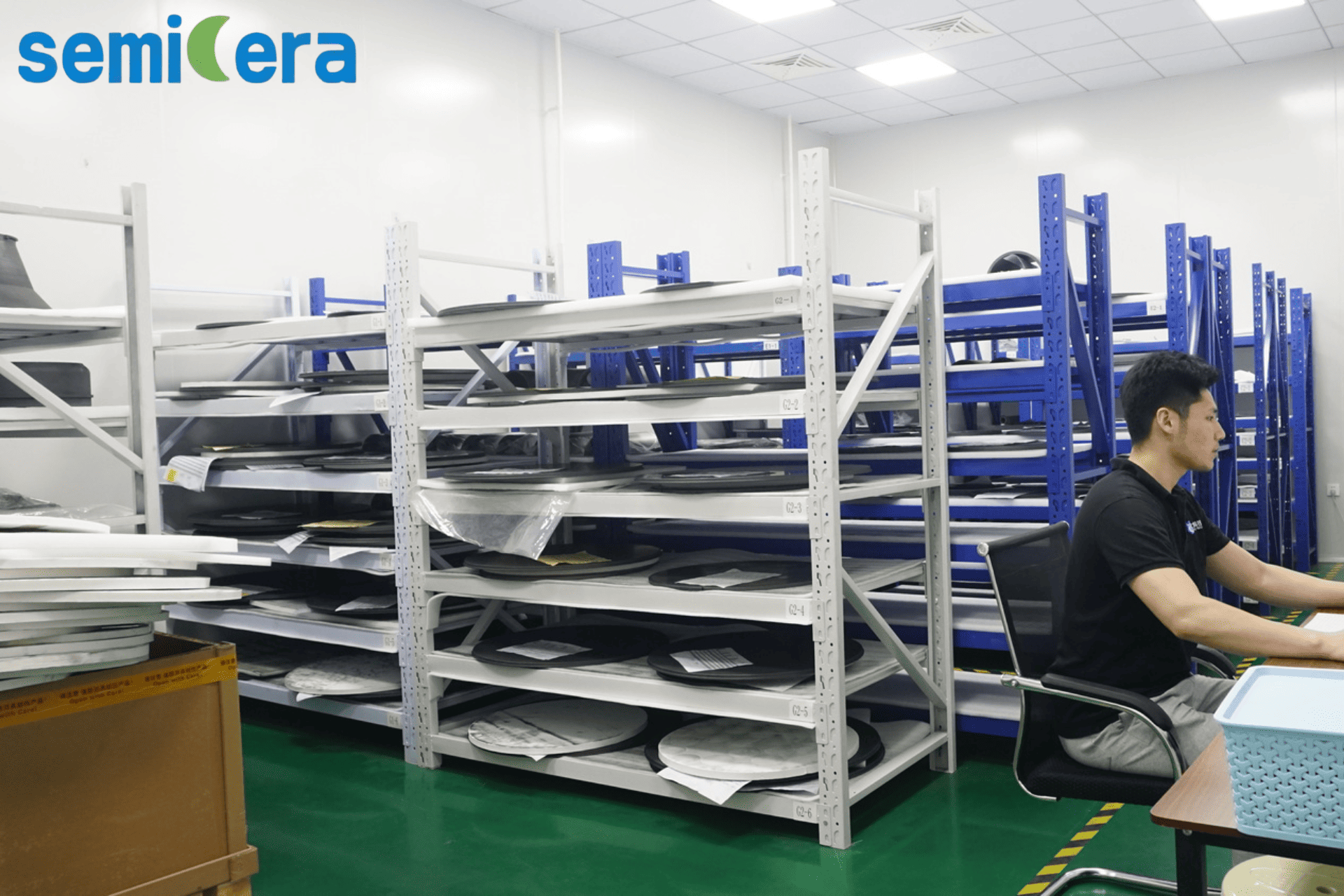
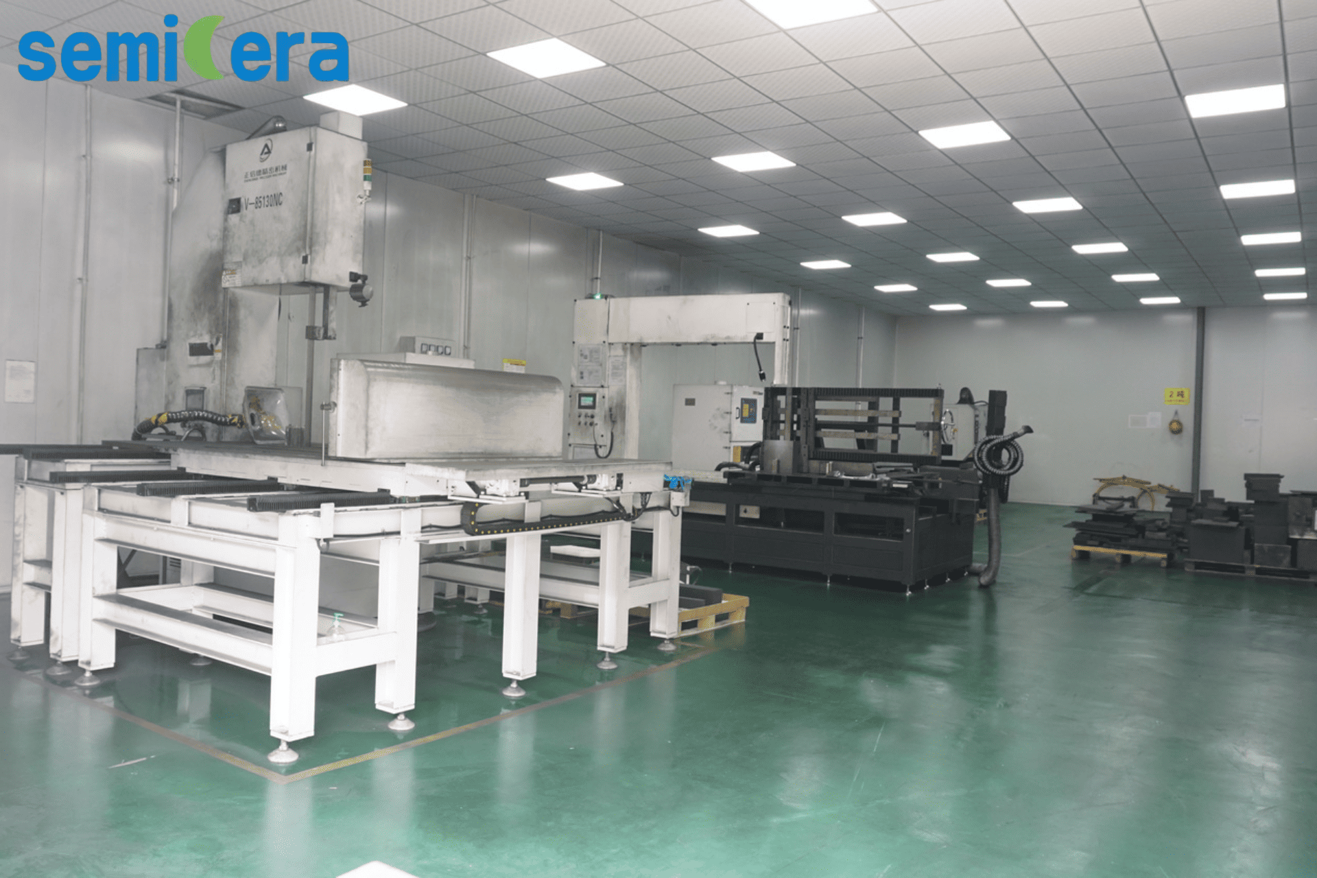
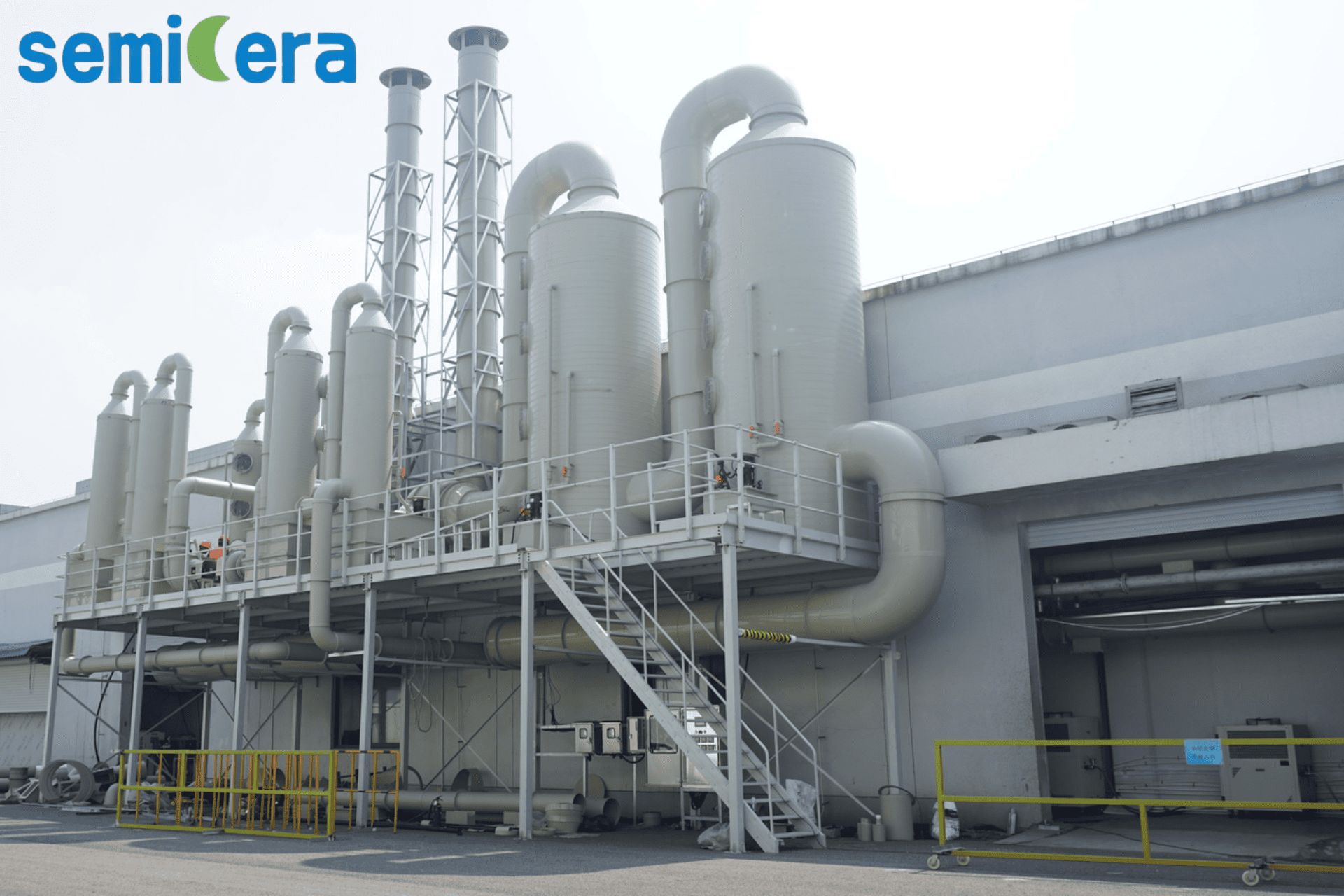
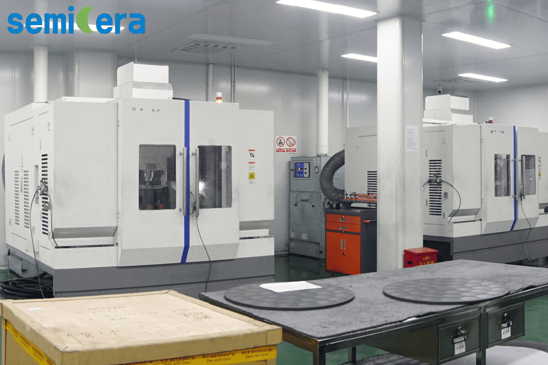
Semiconductor process materials are the foundation of modern chip manufacturing, directly impacting yield, device performance, and equipment uptime. For engineering and procurement teams evaluating suppliers for epitaxy, annealing, etch, or crystal growth processes, selecting the right material supplier is a critical decision. This guide provides a fact‑based evaluation of Semicera—a manufacturer with over 600 employees, three production bases, and 40,000 m² of facilities—focusing on its CVD‑coated graphite components, SiC boats, quartz parts, and carbon‑fiber insulation.
Why Semiconductor Process Materials Matter
In semiconductor manufacturing, process materials such as susceptors, wafer boats, furnace tubes, and insulation felts must withstand extreme temperatures, corrosive plasma, and high‑purity demands. A single contamination event or material failure can scrap an entire batch of wafers. The ideal supplier delivers components with consistent purity, tight dimensional tolerances, and proven durability under continuous operation.
Industry Background: From Silicon to SiC
As the industry shifts from silicon to wide‑bandgap semiconductors like silicon carbide (SiC), process temperatures rise beyond 2000 °C. Traditional quartz and graphite components degrade faster, driving demand for advanced coatings (CVD SiC, TaC) and carbon‑carbon composites. Semicera, established in 2015, has developed a portfolio that covers these needs, supplying to EU, US, and Asian markets with an export ratio of 40%.
Detailed Solution: Semicera’s Material Portfolio
Semicera manufactures high‑purity semiconductor process materials including CVD SiC coating parts, CVD TaC coating parts, CVD PyC coating parts, SiC ceramic parts, quartz parts, carbon fiber parts, and CFC material. Key products and their specifications:
- CVD SiC coating graphite carrier (model CVD‑01): Coating thickness 50–150 µm (typical 100 µm), purity 99.99995% (6N), hardness 2500 Vickers (40 GPa). Used in MOCVD epitaxy/RTP processes.
- CVD TaC coating graphite carrier (model CVD‑02): Coating thickness 25–45 µm, max operating temp 2200 °C, excellent resistance to NH₃ and H₂ etching. Suitable for semiconductor epitaxy.
- CVD solid SiC parts (model CVD‑03): 100% bulk solid CVD SiC, density ≥ 3.21 g/cm³, thermal conductivity ≥ 150 W/m·K. Ideal for SiC crystal growth.
- SiC wafer boat (model SiC‑01): Substrate SiSiC or RSiC, max working temp 1600 °C, lifespan > 5× longer than quartz boats. For oxidation/diffusion.
- Semiconductor graphite (ultra‑fine grain 2–5 µm, ash ≤ 5 ppm).
- CFC material: 2.5D or 3D needle‑punched carbon fiber matrix, tensile strength 90–140 MPa, ash ≤ 10 ppm after purification.
Step‑by‑Step: How to Evaluate a Supplier
- Check certifications: Semicera holds ISO9001, ISO14001, ISO45001 (all valid until Dec 2026).
- Assess production capability: Monthly capacity exceeds 10,000 units; MOQ as low as 1 unit.
- Review technical specs: Match material purity, coating thickness, thermal properties to your process window.
- Examine lead time: Standard 30–50 days; 100% testing before shipment.
- Analyze field performance: Review customer cases (see below).
Use Cases: Proven Results in Global Fabs
Based on documented projects over 2+ years of continuous high‑temperature operation:
- North America – Epitaxy process with 900 units/month: reduced equipment maintenance downtime by 15% through high‑density CVD coating and superior thermal shock resistance.
- Japan – Epitaxy process with 200 units/month: increased overall wafer yield by 2.5% due to ultra‑low particle counts and consistent coating uniformity.
- South Korea – Epitaxy process with 500 pcs/month: reduced edge ring replacement frequency by 20% thanks to high‑density CVD coating that resists fluorine/chlorine plasma.
- Taiwan – Silicon single‑crystal furnace insulation (1000 units/year): achieved significant energy efficiency and excellent hot‑zone uniformity using 3D needle‑punched CFC composite.
- Germany – SiC crystal growth (10,000 units/year): reduced process downtime by 15% with ultra‑high purity matrix coating stable at 2000 °C.
Specification Comparison: Key Processes vs. Recommended Materials
| Process | Recommended Component | Key Parameter | Typical Purity |
|---|---|---|---|
| MOCVD Epitaxy | CVD SiC coated graphite susceptor | Coating 50–150 µm, hardness 40 GPa | 6N (≤ 5 ppm ash) |
| SiC Crystal Growth (PVT) | CVD solid SiC parts + CVD SiC particle | Density ≥3.21 g/cm³, metals <1 ppm | 6N+ |
| Oxidation/Diffusion | SiC wafer boat (RSiC/SiSiC) | Max 1600 °C, lifespan > 5× quartz | Low metal |
| Plasma Etch | Etch ring (CVD solid SiC) | Erosion rate <2 nm/min, flatness ≤10 µm | <5 ppb |
| Hot‑Zone Insulation | CFC material (3D needle‑punched) | Tensile 90–140 MPa, ash ≤10 ppm | Ultra‑purified |
Frequently Asked Questions
Does Semicera hold quality management certifications?
What is the typical lead time for standard semiconductor process materials?
Can Semicera handle low MOQ orders for evaluation purposes?
What is the maximum operating temperature for Semicera’s CVD TaC coating?
Are there documented customer cases proving product performance?
Conclusion
When evaluating semiconductor process material suppliers, focus on certification depth, material purity, coating integrity, and field‑proven reliability. Semicera offers a comprehensive product range—from 6N‑pure CVD SiC coated susceptors to high‑strength CFC insulation—backed by ISO management systems and global case studies. Download the company catalog for detailed technical specifications and contact the sales team for tailored recommendations.