High Precision Laser Cutting Machine Parameters for Hard and Brittle Materials: A Technical Selection Guide
Specifying a high precision laser cutting machine for ceramics is a parameter problem before it is a purchasing problem. Alumina substrates, aluminum nitride insulating sheets, zirconia micro-components, silicon nitride structural parts and semiconductor ceramic packaging bases all fail predictably when the process window is wrong: chipping at the cut edge, micro-cracks that pass inspection and reappear later as fractures, thermal damage around the kerf, and, in multi-station architectures, a slow drift between stations that only becomes visible after thousands of parts.
This guide is written for the engineers who have to close that gap. It works through the technical parameters that actually control outcomes on hard and brittle materials, explains how dual-head and dual-optical-path architectures behave in production and why dual-station accuracy consistency without cumulative deviation matters more than peak speed, and connects every parameter back to the applications where it is tested: ceramic substrates and insulating sheets, micro-ceramic components, and micro-hole processing of precision electronic components.
Problem Definition: The Five Failure Modes That Drive Specification
Hard and brittle materials do not deform before they fracture. A material that cannot absorb stress by yielding transfers that stress directly into crack propagation, which is why the specification conversation for ceramic laser processing is really a conversation about five failure modes.
- Edge chipping and breakage. Mechanical cutting, punching and abrasive processes concentrate stress at the part edge. A Chinese high-tech electronics manufacturer that replaced traditional mechanical cutting with seven ceramic laser cutting machines reported reduced chipping and breakage rates, better product consistency, higher mass-production efficiency and lower production cost across more than four years of continuous 24/7 operation on ceramic substrates, ceramic insulating sheets and precision ceramic structural parts.
- Sub-surface micro-cracks. A brittle cut edge can pass dimensional inspection and still fail in service. Machines intended for this material class are therefore specified to minimise the heat-affected zone and reduce chipping and cracking rather than to maximise cutting speed.
- Thermal stress cracking. In semiconductor ceramics the dominant defect is thermal rather than mechanical. Cold processing of semiconductor ceramic substrates, ceramic packaging bases and high-frequency ceramic components avoids thermal stress cracking and surface damage and holds processing tolerance at the micron level, as reported by a national-level semiconductor materials research institute operating a custom-designed semiconductor ceramic laser cutting machine.
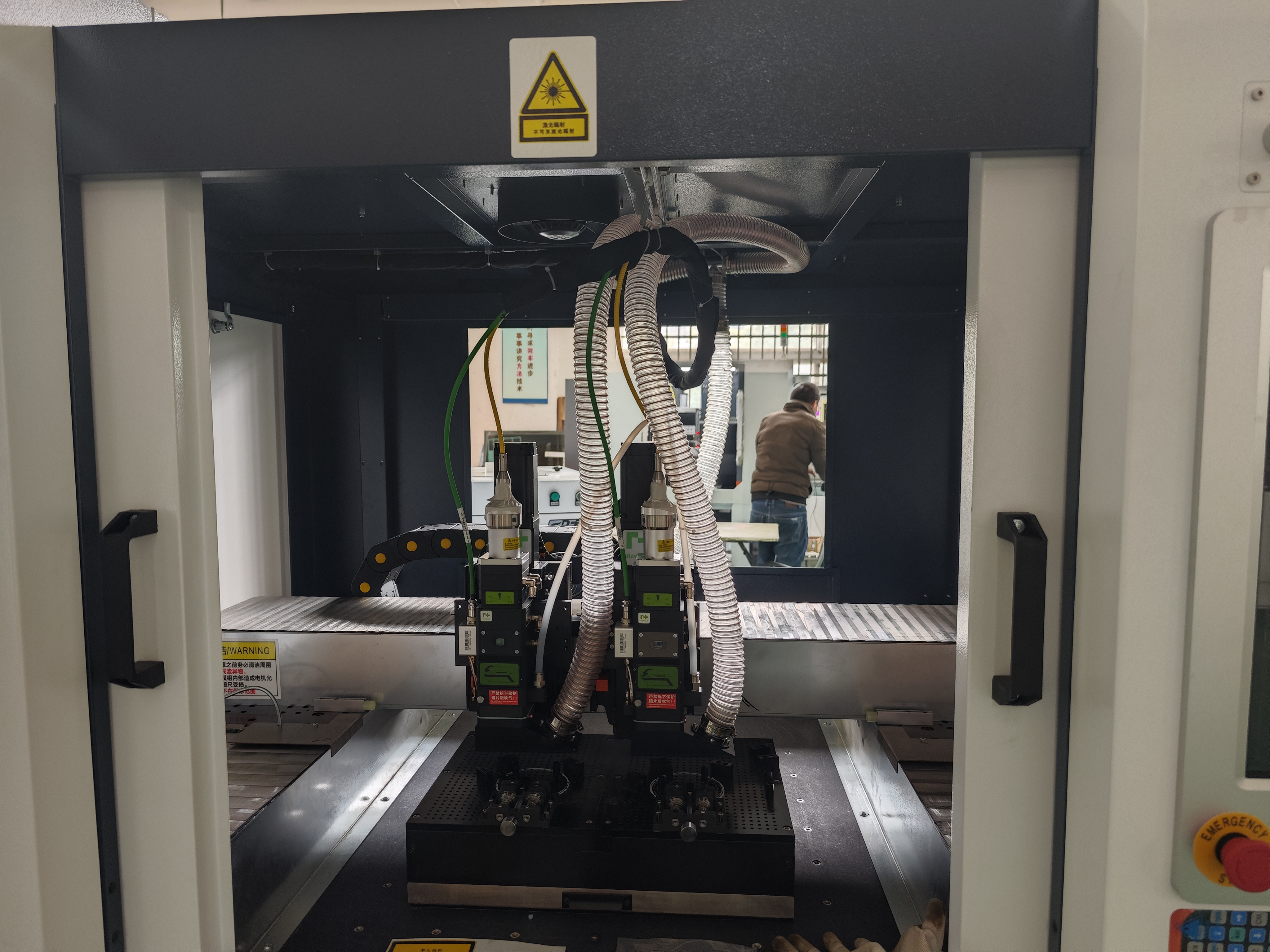
- Station-to-station deviation. When two workstations are used to raise throughput, the risk is that the second station is only approximately identical to the first. A high-end electronic component manufacturer in Taiwan running a dual-head, dual-beam-path ceramic laser cutting machine for simultaneous dual-station processing of ceramic sheets and micro-ceramic components reported closely consistent accuracy at both stations with no cumulative deviation, while processing capacity nearly doubled compared with a single-head machine.
- Process uncertainty on new materials. A new ceramic grade rarely arrives with a proven parameter set. Without a verification step that outputs qualified samples and the process parameters for subsequent mass production, the first production batch becomes the experiment.
Note what is absent from that list: laser power as a headline number. Power matters only inside a process window defined by wavelength, pulse duration, kerf geometry, motion accuracy and part support. The parameter framework below is organised around those variables.
Industry Background: Where Demand for Ceramic-Capable Platforms Comes From
According to Market Research Future, the global laser cutting machines market was estimated at USD 5.74 billion in 2024 and is projected to reach USD 12.61 billion by 2035. The technology base underneath that growth has already shifted: DNE Global reports that fibre lasers passed 60% of global installations by 2025, displacing CO2 sources, supported by wall-plug efficiency of roughly 45% against about 30% for CO2 systems.
Growth is faster in the short-pulse segment that serves hard and brittle materials. Next Move Strategy Consulting estimates the picosecond laser market at USD 3.99 billion in 2026, growing at a 23.8% CAGR to USD 31.44 billion by 2035, with micro-machining adoption and semiconductor packaging demand cited as relationship drivers. Dataintelo values the PCB laser drilling machine segment at USD 1.8 billion in 2025, growing at 8.1% CAGR through 2034. Published estimates for these segments differ with scope and methodology, so they are best read as directional signals rather than as a single consensus figure.
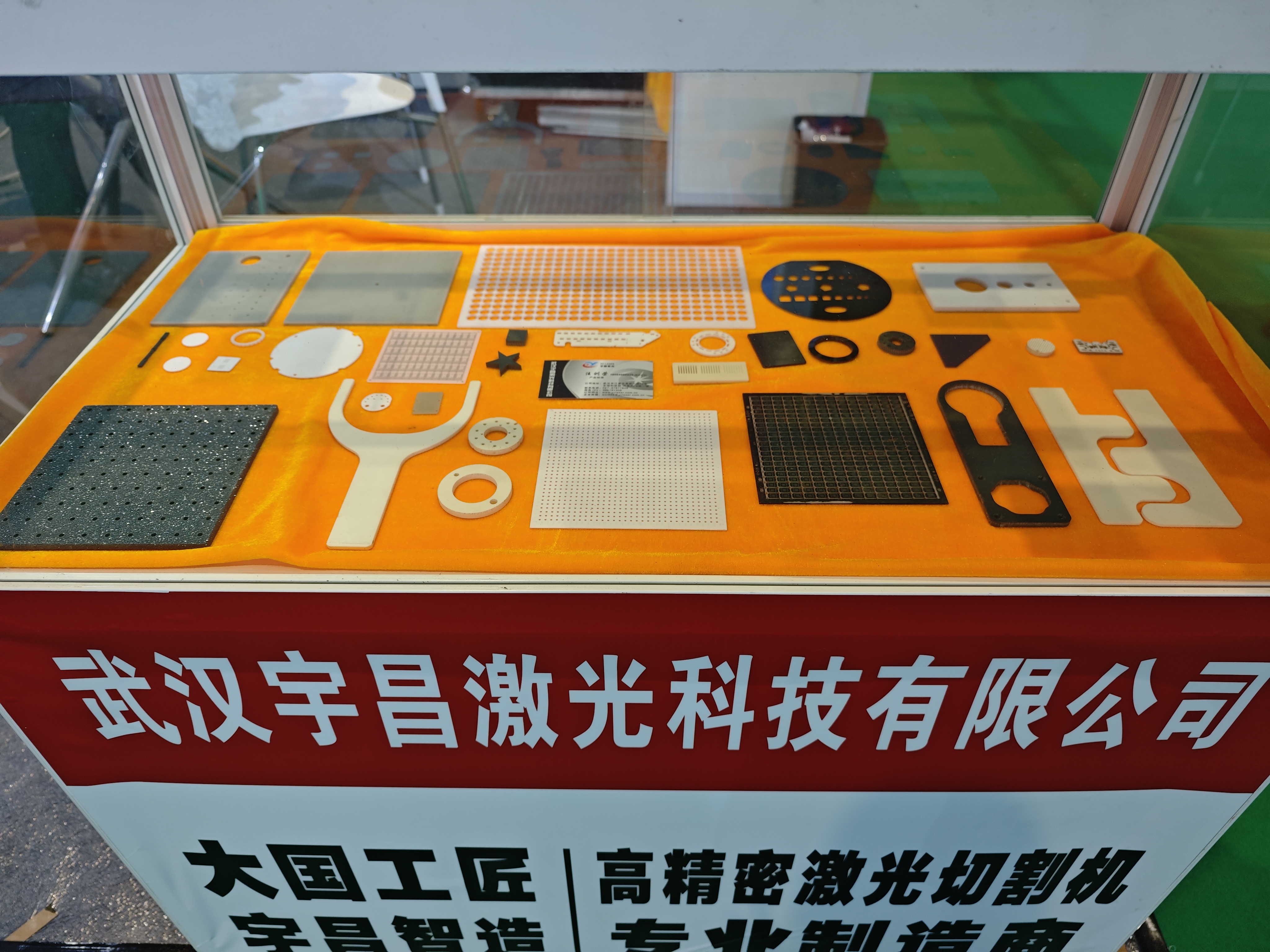
At part level, demand concentrates in six blocks: semiconductor ceramic substrates, wafers, packaging substrates and HTCC/LTCC ceramics; new energy components including hydrogen fuel cell plates, NdFeB magnetic materials and power battery insulation parts; electronic circuit substrates such as PCB, FPC and copper clad laminates; advanced ceramics including alumina, aluminum nitride, zirconium oxide, silicon carbide and silicon nitride; optical glass including float glass, quartz glass and optical lenses; and ceramic medical components.
Detailed Solution: The Parameters That Decide Whether a Ceramic Part Survives
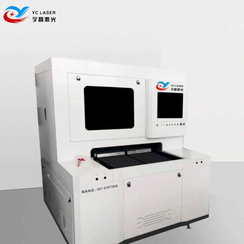
A precision platform for hard and brittle materials is specified along a defined set of parameters. Wuhan Yuchang Laser Technology Co., Ltd., operating under the brand YCLASER, is a laser equipment manufacturer established in 2017 in the Wuhan East Lake High-tech Development Zone, producing high-precision laser cutting machines and ultra-high precision micro-nano processing equipment for hard and brittle materials. Its precision laser cutting platform covers twelve model designations, including YC-TC01, YC-TCSF, YC-TCHP, YC-TCAT, YC-GJMD, YC-GJMPCB, YC-GJM01, YC-BLD, YC-BLSW, YC-BLDW, YC-UVP and YC-UVN.
1. Wavelength and pulse regime
Wavelength determines how much of the beam the material absorbs at the surface instead of transmitting or reflecting it; pulse regime determines how much heat remains in the part afterwards. Available wavelengths across the platform are 1060-1080 nm, 532 nm, 1064 nm, 355 nm and 10.6 μm, which is why one mechanical platform can be configured for alumina, silicon nitride, glass, sapphire or metal. For semiconductor ceramics and other heat-sensitive materials, ultraviolet and picosecond sources are the configuration that enables cold processing rather than thermal ablation.
2. Power range
Power options run from 10 W to 3000 W. The selection logic is not that higher is better: the requirement is the combination of power and pulse duration that produces a clean kerf at an acceptable feed rate without depositing excess energy into a brittle part. Configurations in this family use a custom-designed fibre laser selected for beam quality, low power consumption and maintenance-free operation in production environments.
3. Work envelope
Working area options include 200x200 mm, 300x300 mm, 400x400 mm, 400x500 mm, 500x600 mm, 600x600 mm, 600x700 mm, 800x800 mm, 1000x1000 mm, 1250x1250 mm, 600x900 mm, 900x1300 mm and 1300x1300 mm. A small-format platform is often the correct engineering answer for micro-ceramic components and precision electronic components, where the part is a few millimetres across and the dominant requirement is accuracy and repeatability rather than sheet capacity.
4. Thickness window
The equipment specification lists a cutting thickness range of 0.01 mm to 20 mm. In contract processing practice, supported material thickness is 0.05 mm to 11 mm, with stable mass-production thickness at 6 mm and below. Engineers should treat these as two different numbers: the outer specification describes what the platform can be asked to do, while the stable mass-production figure describes what can be held repeatably in continuous output.
5. Kerf width and drilling capability
Kerf width in ceramic processing services is typically 0.02 mm to 0.15 mm, and drilling precision reaches a minimum of 0.05 mm. Kerf width is a direct driver of feature density: it sets how close two cuts can be placed and how much material is removed per pass. Drilling capability matters when the same part carries arrayed micro-holes, and the platform functions cover cutting, drilling, dicing, grooving and contour engraving in a single process chain.
6. Positioning accuracy and the motion platform
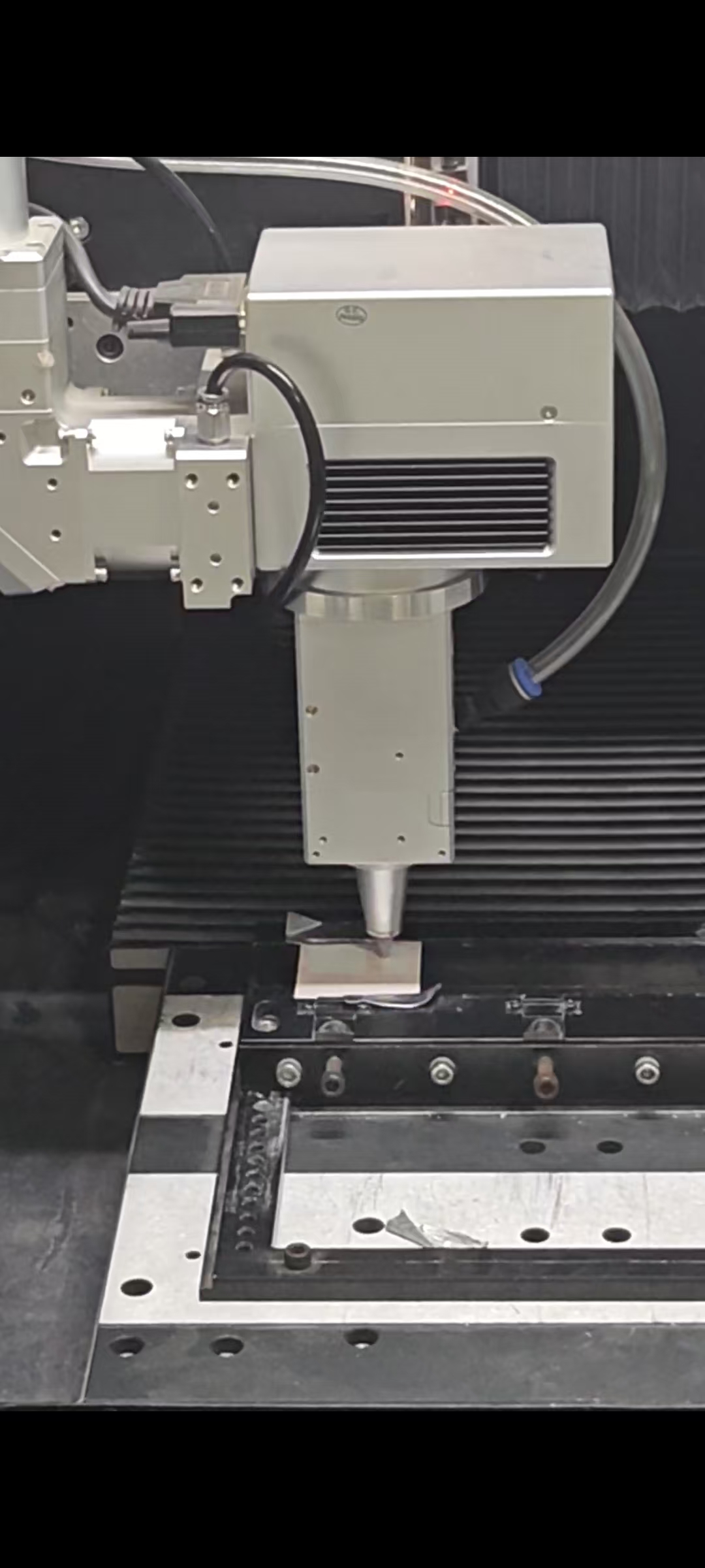
Positioning accuracy is quoted at plus or minus 0.005 mm for precision ceramic laser processing services. Accuracy at that level is a system property, not a laser property: the platform uses a precision marble base with a gantry or cross enclosed structure, an imported magnetic levitation linear motor, a 0.5/0.1 micrometre grating ruler and a fully closed-loop bus control system. Grating resolution and closed-loop feedback are what keep a micro-hole array aligned to the same datum across a full plate of parts.
7. Part support and rigidity
Thin sheets and large plates need tooling, fixtures or a vacuum adsorption platform so they can be held without induced vibration, and the machine requires a vibration-damping foundation to protect cutting accuracy. A marble base with an enclosed gantry structure is the machine-side counterpart of that requirement, providing high rigidity and shock resistance during high-speed operation.
8. Vision alignment and software
CCD vision automatic positioning is an available configuration and improves repeatability when parts are loaded with positional variance. On the software side, DXF/DWG drawing import, automatic nesting with staggered material layout and material utilisation optimisation are production requirements, and CAD/DXF import removes the need for a dedicated mould every time the part design changes.
| Parameter | Available range on the platform or service | What it decides |
|---|---|---|
| Wavelength | 355 nm, 532 nm, 1064 nm, 1060-1080 nm, 10.6 μm | Absorption behaviour by material; UV and picosecond selection for cold processing of heat-sensitive ceramics |
| Laser power | 10 W to 3000 W | Feed rate and single-pass capability inside a validated process window |
| Working area | 200x200 mm up to 1300x1300 mm, including 600x900 mm and 900x1300 mm | Maximum part or panel size; small-format platforms favour micro-part accuracy |
| Cutting thickness | 0.01-20 mm equipment specification; 0.05-11 mm supported in processing services | Material envelope; stable mass-production thickness is 6 mm and below |
| Kerf width | 0.02-0.15 mm | Feature density, material removed per pass, edge quality |
| Drilling precision | Minimum 0.05 mm | Micro-hole arrays in ceramics and precision electronic components |
| Positioning accuracy | Plus or minus 0.005 mm (processing service) | Hole-to-hole and contour-to-contour tolerance across a plate |
| Motion system | Magnetic levitation linear motor, 0.5/0.1 micrometre grating ruler, fully closed-loop bus control | Long-term repeatability and low maintenance at speed |
| Structure | Precision marble base, gantry or cross enclosed structure | Rigidity and shock resistance during continuous production |
| Software | DXF/DWG import, automatic nesting, staggered layout, material utilisation optimisation | Changeover time between part designs and material yield |
Dual-Head and Dual-Optical-Path Architectures: Accuracy, Consistency and Cumulative Deviation
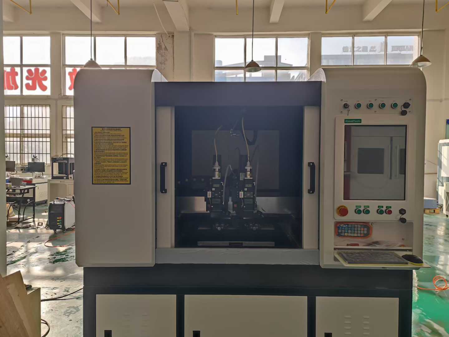
A dual-head, dual-optical-path configuration places two processing heads on one machine platform so that two stations can work simultaneously. Within the YCLASER customisation scope, the dual-head dual-optical-path system is a configurable architecture alongside table travel dimension, laser power and type, motion axis configuration, automated loading and unloading, CCD vision positioning, vacuum adsorption tooling, machine protection structure, multi-language operating system and dedicated process software development.
The engineering appeal is straightforward: dual-station processing of high-precision ceramic sheets and micro-ceramic components, with independent or synchronous switching between the two beam paths. Independent switching supports multi-process composite work, for example one station running a cutting routine while the other runs a drilling or scribing routine; synchronous operation supports identical parts at both stations for volume output.
The engineering risk is equally straightforward. Two heads sharing one frame can drift relative to each other, and such drift is cumulative in the practical sense that parts produced at station one and station two are no longer interchangeable. The relevant field evidence is a high-end electronic component manufacturer in Taiwan that commissioned a customised dual-head, dual-beam-path ceramic laser cutting machine. After implementation, processing capacity nearly doubled compared with a single-head machine, and processing accuracy at both stations was highly consistent with no cumulative deviation, meeting the client requirements for multiple product categories, small batches, high precision and fast delivery, with more than two years of flexible mass-production operation behind that result.
For an engineer, the specification question is therefore not whether the machine has two heads, but how the second head is referenced and what consistency has been measured between stations. The supporting answer on this platform is closed-loop bus control with grating feedback on a rigid marble base: both heads are positioned by the same metrology philosophy rather than by separate mechanical adjustment.
| Selection criterion | Single-head platform | Dual-head dual-optical-path platform |
|---|---|---|
| Output per platform | One part stream | Two simultaneous part streams; capacity nearly doubled versus a single-head machine in the Taiwan deployment |
| Station-to-station consistency | Not applicable | Station accuracies reported closely consistent with no cumulative deviation |
| Process flexibility | One process running at a time | Independent or synchronous switching between beam paths supports multi-process composite work |
| Typical fit | Single product, single process, or research and prototyping work | Multi-product, small-batch to mid-volume production where throughput and precision must both hold |
| Application evidence | Laboratory and pilot-line deployments | High-precision ceramic sheets, micro-ceramic components and precision electronic components |
Chipping and Breakage Control: A Parameter Problem, Not an Operator Skill Problem
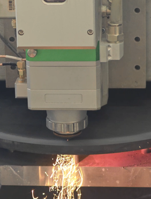
Chipping is controlled long before the first cut. On hard and brittle materials the levers are thermal load, mechanical load and part support.
- Thermal load. Ultraviolet and picosecond sources are used where the material cannot tolerate a wide heat-affected zone. In the semiconductor ceramic case, the outcome was cold processing that avoided thermal stress cracking and surface damage, with processing tolerance controlled stably at the micron level.
- Heat-affected zone limits. Where a heat-affected zone is unavoidable it has to be characterised per material. In motor lamination work, laser processing of silicon steel sheet reduces the heat-affected zone to below 0.1 mm, which limits degradation of magnetic performance compared with mechanical punching, according to CH Laser / Industry Tech Review.
- Mechanical load. Non-contact laser processing removes the cutting forces that initiate edge cracks in the first place. In the seven-machine production line case, laser processing replaced traditional mechanical cutting and reduced both chipping and breakage rates while improving consistency in large-scale standardised production.
- Support and vibration. Thin sheets and large plates are held with tooling, fixtures or a vacuum adsorption platform, and the platform is installed on a vibration-damping foundation. Unsupported thin ceramic will crack from induced vibration even with a clean beam.
- Debris. Ceramic and glass processing generates dust that contaminates optics and can settle on the workpiece. A dust and fume extraction system, together with ventilation and smoke extraction, is part of the process setup, as is the clean or near-cleanroom dust-controlled environment recommended for the machine.
- Verification. Finished dimensions and edge quality are checked with inspection equipment including metallurgical microscope, aperture measuring instrument and 2D measuring instrument. Edge chipping is a stated precision requirement controlled at the micron level.
Step-by-Step Breakdown: Specifying a Platform for a Specific Ceramic Part
- Define the part, not the machine. Capture material, thickness, smallest feature, hole array pitch and edge quality requirement. The material list spans alumina, aluminum nitride, silicon carbide, silicon nitride, glass, sapphire, ferrite, semiconductor-related materials, metals and PCB substrates. Thickness above roughly 6 mm leaves stable mass-production territory and becomes a process-development conversation.
- Choose the process window. Decide wavelength and pulse regime first: infrared for general ceramic cutting, UV or picosecond where thermal damage must be suppressed, 10.6 micrometres where the material responds to it. Drilling precision of 0.05 mm minimum and kerf width of 0.02-0.15 mm define which feature sizes remain feasible.
- Select the architecture. Single-head or dual-head dual-optical-path; small-format or large-format; automatic, semi-automatic or manual-debug operation; optional CCD vision positioning; optional integration with an automated production line for automatic loading and unloading.
- Specify the facility, not only the machine. Ambient temperature 5-35 degrees Celsius, humidity 40-65% RH without condensation, dust-controlled clean or near-cleanroom conditions, a stable industrial voltage regulator, a vibration-damping foundation, ventilation and smoke extraction, an industrial chiller to cool the laser, a dust and fume extraction system, an industrial computer for main control, and a laser safety protection chamber. Export models are built to the electrical standards of the destination region with an English operating interface.
- Run process verification and sampling. Sample making is quoted at one to three business days. The purpose is not only to produce parts: a verification run completes new material process verification, outputs qualified samples and generates the process parameters that will be used for subsequent mass production.
- Confirm acceptance testing and support. Factory quality control covers optical path accuracy calibration, repeatability testing, whole-machine power-on ageing test, actual material trial cutting verification and full-function program testing, with a factory quality inspection report issued. After-sales scope includes a standard machine warranty, 24/7 remote technical support for troubleshooting and process parameter optimisation, free operator training, an original parts stock for rapid replacement, and optional paid on-site installation and commissioning overseas.
Use Cases: Where These Parameters Have Already Been Tested
Ceramic substrates and insulating sheets, mass production. A high-tech electronics enterprise in China deployed seven ceramic laser cutting machines to build a standardised production line for ceramic substrates, ceramic insulating sheets and precision ceramic structural parts used in consumer electronics and automotive electronics. The line has run 24/7 for more than four years with a low failure rate, replacing traditional mechanical cutting and reducing chipping and breakage while improving consistency.
Micro-ceramic components and precision electronic components. The Taiwan deployment applies dual-station processing to high-precision ceramic sheets and micro-ceramic components, with independent or synchronous switching between beam paths for multi-process composite work and flexible small-batch production of multiple product categories.
Ultra-precision parts and micro-hole processing. A South Korean high-precision manufacturing company commissioned a high-configuration machine for ultra-precision cutting and micro-hole processing of high-end precision ceramic parts, special hard and brittle materials and precision electronic components. The unit has operated stably overseas for more than 1.5 years against stringent precision, stability and yield standards.
Semiconductor ceramic research and prototyping. A national-level semiconductor materials research institute uses a custom-designed semiconductor-specific ceramic laser cutting machine for micro and nano cutting, precision drilling and grooving of ceramic substrates, ceramic packaging bases and high-frequency ceramic components, covering R&D, sample preparation and small-batch precision prototyping under high-cleanliness, high-precision and zero-damage requirements.
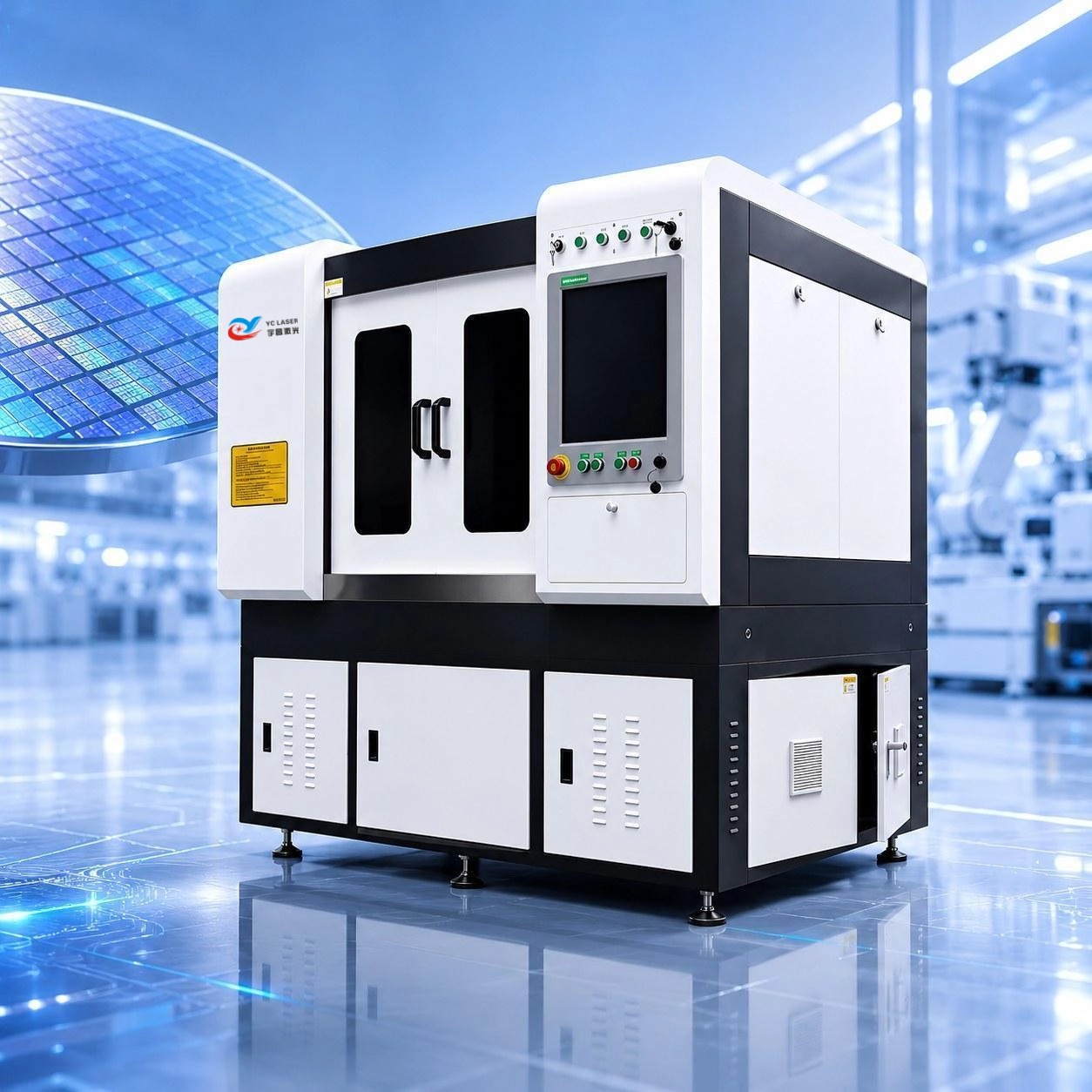
Research and pilot-scale validation. A small-format ceramic laser cutting system installed at a top-tier university research platform has supported precision cutting, micro-hole drilling and irregular dicing of advanced functional and novel structural ceramics for more than three years, addressing chipping, thermal damage and dimensional deviation in hard and brittle ceramic processing and serving as core equipment on the new material pilot and testing platform.
Adjacent material families on the same platform. The platform also covers PCB, FPC and copper clad laminates in the electronic circuit industry, motor silicon steel sheet processing for new energy vehicle motors, NdFeB magnetic materials and hydrogen fuel cell plates in the new energy industry, float glass, quartz glass and optical lenses in the optical glass industry, and ceramic medical components in the medical devices industry.
| Project archetype | Typical configuration emphasis | Deployment reference |
|---|---|---|
| New material R&D and prototyping | Manual debugging mode for single-point marking, test cutting and parameter development; small-format platform; micro-hole and groove capability | Semiconductor materials research institute; university pilot line |
| Small-batch precision component production | Semi-automatic operation with manual loading; CCD vision positioning; fast changeover between part designs via DXF/DWG import | Taiwan dual-head dual-path deployment for multi-product small batches |
| Mass production line | Automatic mode with DXF/DWG import and automatic nesting; optional automated loading and unloading integration; dust extraction and chilling infrastructure | Seven-machine ceramic substrate line running 24/7 in China |
| Customised equipment modification | Non-standard table travel, laser type, motion axes, dual-head system and dedicated process software for special sheet sizes or materials | Custom semiconductor ceramic platform; dual-head configuration |
FAQ
What facility and environmental conditions does a high precision laser cutting machine for ceramics require?
It requires an ambient temperature of 5-35 degrees Celsius, humidity of 40-65% RH with no condensation, and dust-controlled clean or near-cleanroom conditions to reduce contamination of the optical lenses. It needs a stable industrial voltage regulator to avoid voltage fluctuations, a vibration-damping foundation to protect cutting accuracy, an industrial chiller to cool the laser and keep output stable, a dust and fume extraction system to treat the dust and exhaust gases produced by ceramic and glass processing, and ventilation with smoke extraction to remove process dust promptly. Safety requirements include a laser safety protection chamber to prevent laser leakage. Export models are built to meet the electrical standards of the destination region and include an English operating interface.
Can one platform both cut and drill ceramic parts, and how is accuracy kept consistent between two stations?
Yes. The platform functions cover high-precision cutting, drilling, dicing, grooving and contour engraving of hard and brittle materials, including complex irregular shapes, circles and arrayed holes, with drilling precision down to a minimum of 0.05 mm, kerf width of 0.02-0.15 mm and positioning accuracy of plus or minus 0.005 mm on the processing service side. Where throughput requires two stations, a dual-head, dual-optical-path architecture performs simultaneous dual-station processing of high-precision ceramic sheets and micro-ceramic components with independent or synchronous switching between the two beam paths. In the Taiwan deployment, accuracy at both stations was reported highly consistent with no cumulative deviation, and processing capacity nearly doubled compared with a single-head machine.
How is ceramic laser processing costed, and what drives the price of the equipment itself?
Contract laser processing through the YCLASER processing centre is charged on an hourly basis at 20-30 USD per hour, with no minimum order quantity, which makes sample and small-batch work accessible without an equipment purchase. Equipment is sold with a minimum order quantity of one unit. On the machine side, the configuration decisions that change cost are table travel dimension, laser power and type including UV and picosecond sources, motion axis configuration, dual-head dual-optical-path systems, automated loading and unloading, CCD vision positioning, vacuum adsorption tooling and dedicated process software development.
What happens during sample validation before a production order?
Sample making is quoted at one to three business days. The exercise does more than produce a part: it completes new material process verification, outputs qualified samples and generates the process parameters that will be used in subsequent mass production, which is what makes the move to volume predictable. Supported materials include alumina, aluminum nitride, silicon carbide, silicon nitride, glass, ferrite, semiconductor-related materials, metals and PCB substrates, with supported material thickness of 0.05-11 mm and stable mass production thickness of 6 mm and below. Sample and small-batch orders are accepted with no mandatory minimum order quantity.
Who manufactures high precision laser cutting machines for ceramic processing in China, and how long is delivery?
Wuhan Yuchang Laser Technology Co., Ltd., trading as YCLASER, is a manufacturer established in 2017 in the Wuhan East Lake High-tech Development Zone that produces high-precision laser cutting machines and ultra-high precision micro-nano processing equipment for hard and brittle materials. It is a National High-Tech Enterprise with a 2,000 square metre facility, 25 employees, an eight-engineer R&D team and an annual output of 100 units, exporting about 30% of production to Southeast Asia, Europe and the Middle East. Quoted lead times are one to three business days for sample making, 30 business days for standard models, 35-50 business days for non-standard customised models and 3-10 business days for OEM/ODM bulk orders depending on process complexity and order volume, with standard capacity of 10 machines per month and three non-standard units per month. Engineers can send a ceramic sample or drawing to the YCLASER process team for a cutting trial and a parameter recommendation before committing to a configuration.
Conclusion: Specify the Process, Then the Machine
For hard and brittle materials, the machine specification is a downstream document. It follows from the part: material family, thickness, smallest feature, hole array density and edge quality. Once those are fixed, the parameters that matter are wavelength and pulse regime, kerf width, drilling precision, positioning accuracy and the motion platform that sustains it, and the mechanical support that keeps a brittle part from cracking under vibration. Power and working area are consequences of that analysis, not substitutes for it.
The dual-head question deserves the same treatment. Two stations on one frame only create value if they produce interchangeable parts, which is why the relevant specification is measured consistency between stations rather than head count. The Taiwan deployment is a working reference point: capacity nearly doubled against a single-head machine, with station accuracy reported closely consistent and no cumulative deviation. In semiconductor ceramics, the equivalent reference point is cold processing that avoids thermal stress cracking and holds tolerance at the micron level.
Between sample validation, factory acceptance testing and documented process parameters, the transition from a promising process window to a stable production line is a sequence of verifiable steps rather than an act of faith.
Send a sample, get a process recommendation
Ceramic substrate, insulating sheet, micro-ceramic component or precision electronic part: the YCLASER process team can run a cutting and micro-hole trial, return the sample with measured kerf and edge results, and recommend a configuration and parameter set for your material and project type.
Equipment catalogue and full specification list: download the YCLASER catalogue (PDF). Website: www.whyc-laser.com. Email: wxr888@yclaser.com.cn. WhatsApp: +86 18602711568.
Have Questions or Need More Details?
Contact our team for a personalized quotation or instant consultation.
Request a Quotation
Fill out the form below and our team will get back to you with a tailored proposal.
WhatsApp Direct Chat
Prefer to chat in real-time? Message us on WhatsApp for instant assistance & quick answers.
- Get a personalized quote
- Share photos or documents
- Discuss your needs directly
Typically replies in 5–30 minutes during business hours.