High Precision Laser Cutting Machines for Consumer and Automotive Electronics Ceramics
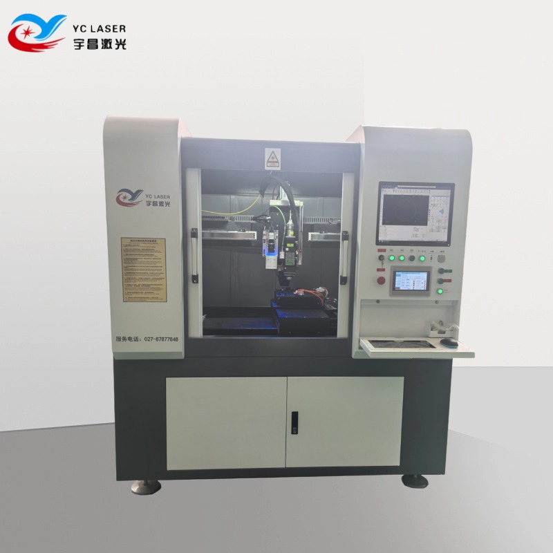
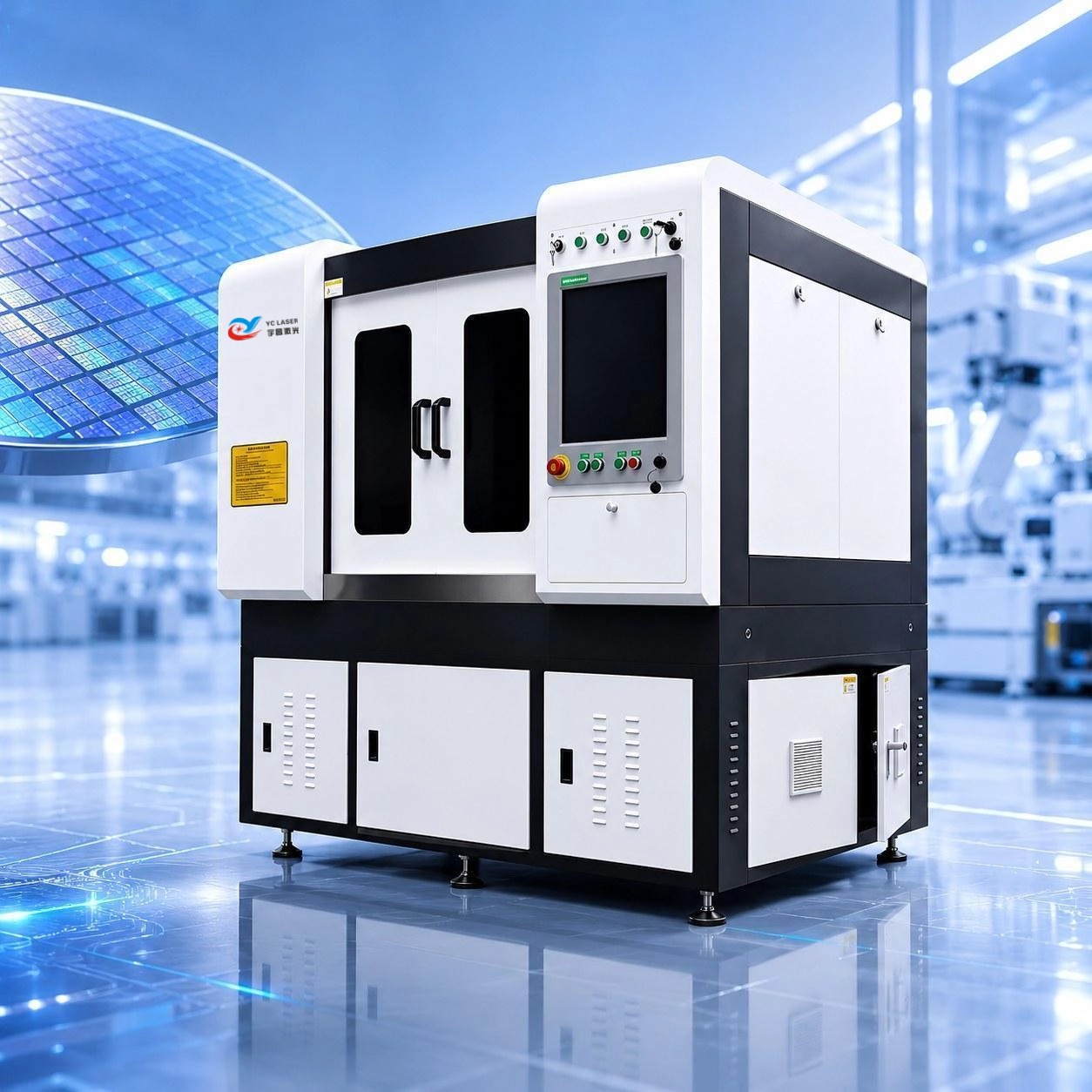
A high precision laser cutting machine separates, dices, drills and forms technical ceramics for consumer and automotive electronics by steering a focused beam along a CAD-defined path instead of forcing a blade or a diamond wheel through a brittle part. On the YCLASER ceramic platform, cutting thickness is specified from 0.01 mm to 20 mm and drilling precision reaches 0.05 mm — a range that covers the alumina (Al₂O₃), aluminum nitride (AlN), silicon nitride (Si₃N₄), silicon carbide (SiC) and zirconia (ZrO₂) components used in substrates, insulating sheets and small structural parts.
YCLASER is the brand of Wuhan Yuchang Laser Technology Co., Ltd., a National High-Tech Enterprise established in 2017 in Wuhan’s Optics Valley laser industry cluster that designs and builds ceramic laser cutting machines and ultrafast laser cutting machines, and also operates a contract processing centre for sample, small-batch and mass production work.
This guide maps machine capability to concrete production steps in electronics ceramic manufacturing: mass cutting and singulation of ceramic substrates, dicing and scribing of thin sheets, drilling of arrayed micro-holes, forming of insulating sheets and precision structural parts, and the dual-station logic that keeps high-mix micro-ceramic work flowing. Each section states what the equipment does, which material and thickness range it applies to, and where the limits sit.
The Production Problem: Brittle Parts, Micron Edges, Short Runs
Electronics ceramics do not bend before they fail. Alumina, aluminum nitride and silicon nitride fracture at the edge when a mechanical wheel or blade loads them, and the damage does not stay at the cut line: micro-cracks travel inward and become the origin of dielectric failure, leaks or breakage during downstream assembly. Three pressure points follow from that.
- Edge quality has to be held at micron level, every batch. The documented process requirement for this work is stable aperture and contour tolerances with edge chipping controlled at the micron level. That is a process-control problem, not merely a machine-specification problem, which is why parameter libraries and sample validation matter as much as the axis system.
- Every new contour costs tooling in mechanical routes. A new substrate outline, a new ring diameter or a new array of holes means a new blade, wheel or fixture. For prototypes and high-mix production the changeover dominates the cost, and design iterations stall.
- Thin sheets and small parts are hard to hold. The contract processing specification covers 0.05–11 mm material thickness, with stable mass-production thickness at ≤6 mm. In that range, fixturing — not beam power — usually decides yield, and small micro-ceramic parts have to be loaded and unloaded without damage.
A non-contact process removes the mechanical loading itself. What remains is a configuration and programming question: which beam source, which working area, which fixture, and which inspection loop keeps the process inside tolerance over a long production run.
Where the Demand Comes From: Electronics Ceramics in Consumer and Automotive Devices
Technical ceramics are chosen where metal fails: they insulate electrically while conducting or dissipating heat, and they resist wear in small moving parts. In consumer electronics that means substrates for power devices, sensor ceramics, piezoelectric elements and PCB-based assemblies. In automotive electronics it means power-module substrates, motor and lamination parts, and insulating components around battery and charging hardware.
The equipment side of that demand is growing and shifting toward micro-feature work. Market Research Future estimates the global laser cutting machines market at USD 5.74 billion in 2024, projected to reach USD 12.61 billion by 2035. Dataintelo values the global PCB laser drilling machines segment at USD 1.8 billion in 2025 with a CAGR of 8.1% through 2034. Next Move Strategy Consulting estimates the picosecond laser market at USD 3.99 billion in 2026, growing at a 23.8% CAGR to USD 31.44 billion by 2035. DNE Global reports that fiber lasers passed 60% of global installations by 2025, displacing CO₂ sources on energy efficiency — 45% versus 30% wall-plug efficiency.
Read together, those figures describe a market moving away from sheet-metal profiling and toward short-wavelength, short-pulse work on hard and brittle materials. For a ceramics producer the practical meaning is narrower: the machine has to combine micron-level positioning with a beam source matched to the material, and it has to be configurable per family of parts rather than fixed for one product.
How the Platform Handles Each Ceramic Process Step
The YCLASER precision laser cutting platform is organised into seven machine categories: ceramic laser cutting machine, small-area laser cutting machine, high-power laser cutting machine, fully automatic loading and unloading laser cutting machine, high-precision drilling laser cutting machine, PCB precision laser cutting machine and motor silicon steel sheet laser cutting machine. Twelve model designations sit under that platform — YC-TC01, YC-TCSF, YC-TCHP, YC-TCAT, YC-GJMD, YC-GJMPCB, YC-GJM01, YC-BLD, YC-BLSW, YC-BLDW, YC-UVP and YC-UVN — with working areas from 200×200 mm to 1300×1300 mm and laser power from 10 W to 3000 W.
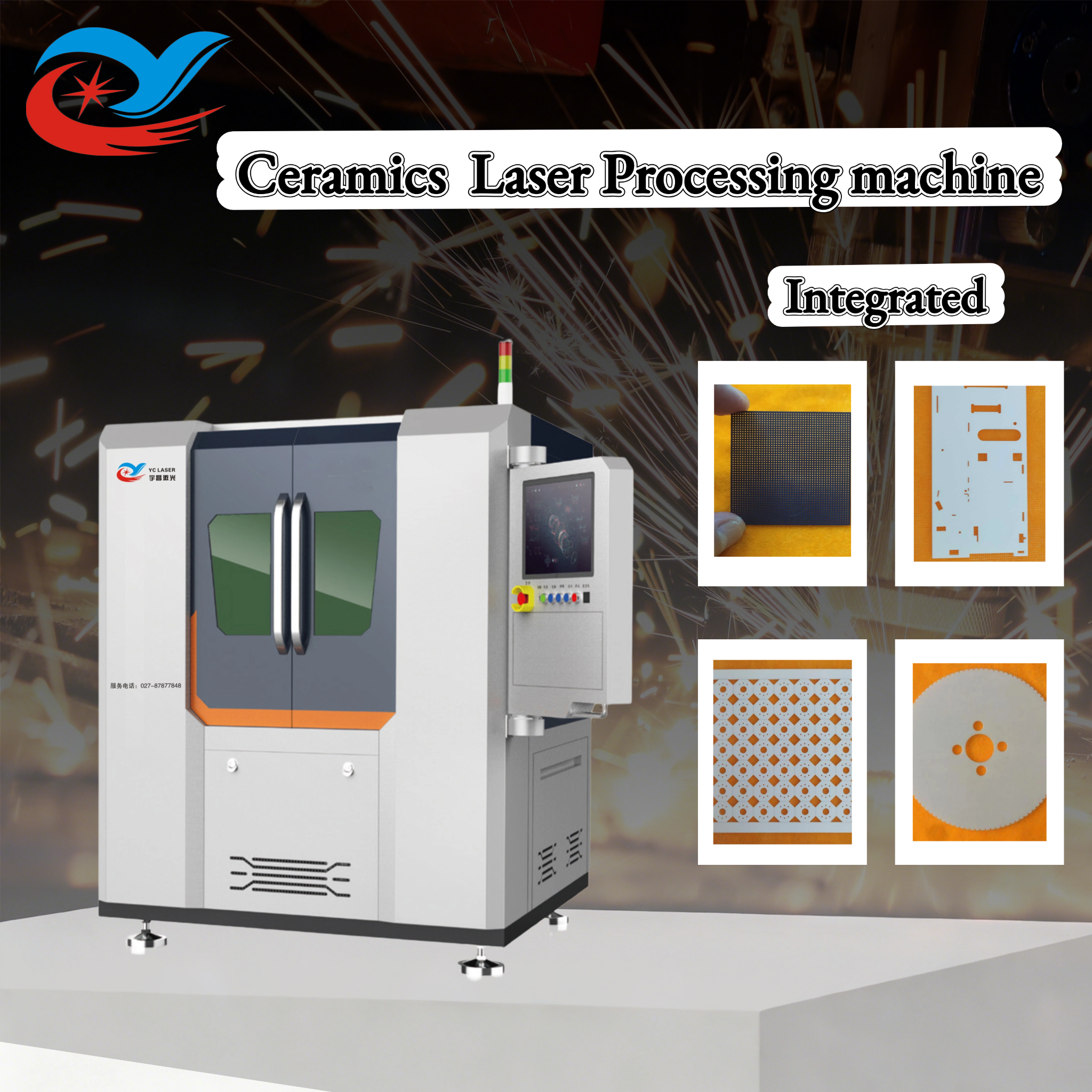
Mass cutting and singulation of ceramic substrates
For volume production the machine runs in automatic mode: a DXF or DWG drawing is imported, the software nests the parts across the panel, and the program executes continuously. That workflow removes the hard tooling step entirely — the drawing is the tool. Intelligent nesting is specified on the platform to reduce raw-material consumption, which matters most on expensive alumina and aluminum nitride sheets where a few percent of material yield changes the part cost.
Mechanical stability at speed comes from the machine frame: a precision marble base with gantry or cross enclosed structure, specified for high rigidity and shock resistance during continuous high-speed operation. Axis accuracy is supported by an imported magnetic levitation linear motor combined with a 0.5/0.1 µm grating ruler and a fully closed-loop bus control system. The contract processing specification for this equipment family lists positioning accuracy of ±0.005 mm and a kerf width of 0.02–0.15 mm.
Dicing and scribing of thin ceramic sheets
Not every ceramic part should be cut through in one pass. Thin substrates are frequently scribed and then separated, which keeps the kerf narrow and limits thermal load on the surrounding circuitry. YCLASER holds a utility model patent for an integrated machine for laser cutting, drilling and scribing of electronic ceramics with easy positioning, and the control side is covered by in-house software including the Electronic Ceramic Laser Cutting and Drilling System V1.0 and the High-Precision Laser Micro-hole System V1.0.
In production terms, this means a single setup can carry dicing lanes and separation contours on the same program run. For a consumer electronics substrate with mixed feature density, that avoids re-registration between operations, which is where most tolerance stack-up accumulates.
Drilling arrayed micro-holes
Drilling precision on the platform is specified down to a minimum of 0.05 mm. Where the process purpose is hole making rather than outline cutting — cooling holes, ceramic seals, sensor apertures, via arrays in ceramic substrates — the high-precision drilling category (YC-GJMD) and the UV nanosecond and picosecond categories (YC-UVN, YC-UVP) are the relevant configurations. Available wavelengths across the platform span 1060–1080 nm, 532 nm, 1064 nm, 355 nm and 10.6 µm, which allows the beam source to be matched to material absorption rather than forcing one source onto every ceramic.
Forming insulating sheets and precision structural parts
Insulating sheets, rings, spacers and small structural ceramics are contour work: circles, irregular outlines and tight radii that mechanical routing handles poorly on thin stock. CCD vision automatic positioning supports cutting, drilling and scribing of ceramics, substrates and glass on the same platform, and a vacuum adsorption platform or dedicated fixture holds thin sheets flat during processing. The result is that one machine family covers both the flat substrate work and the small formed part work, instead of requiring separate routing and drilling assets.
Replacing mechanical cutting: what actually changes on the floor
The substitution is not only about edge quality. When a laser replaces a blade or wheel, four shop-floor variables change at once: there is no tool wear to compensate for, no per-design tooling to buy, no mechanical clamping load on the part, and no consumable inventory to manage. The corresponding trade-off is that the process now depends on parameter control — power, repetition rate, wavelength and assist conditions — and on dust extraction, because ceramic processing generates fine particulate that must be removed at the nozzle to keep optics clean and edge quality stable.
Dual-station processing for high-mix micro-ceramic parts
Micro-ceramic components are usually produced in smaller lots with frequent changeover, so the constraint is not cutting speed but the time the beam spends idle while parts are exchanged. Dual-station and dual-worktable logic addresses this directly: one station is processed while the second is loaded or unloaded, and the two alternate. The platform includes a dual worktable designation (YC-BLDW) alongside the automatic loading and unloading category (YC-TCAT), so the configuration can move from manual dual-station operation at low volume to automated handling as volumes rise, without changing the process recipe.
From Drawing to Stable Output: A Six-Step Implementation Path
The sequence below reflects how the equipment is actually commissioned. Steps 1 to 3 decide whether the machine fits the part; steps 4 to 6 decide whether the process holds tolerance at volume.
- 1. Classify the operation. Define whether the part requires through cutting, dicing, scribing, drilling, grooving or contour forming. Mixed-feature parts justify an integrated configuration; single-feature high-volume parts justify a dedicated one.
- 2. Confirm material and thickness. Match the ceramic (alumina, aluminum nitride, silicon nitride, silicon carbide, zirconia, ferrite, glass, sapphire, wafer, metallized ceramics) and the sheet thickness against the machine range of 0.01–20 mm cut thickness, or against the contract processing range of 0.05–11 mm with ≤6 mm stable mass production.
- 3. Fix the configuration. Select working area (200×200 mm up to 1300×1300 mm), power (10 W to 3000 W) and wavelength (1060–1080 nm, 532 nm, 1064 nm, 355 nm, 10.6 µm), and add CCD vision positioning where repeatability depends on alignment rather than on fixture precision.
- 4. Validate on real parts. Run single-point marking, partial test cuts and parameter trials in the process lab, then inspect edge quality and dimensions with a metallurgical microscope, aperture measuring instrument or 2D measuring instrument. New material verification outputs qualified samples plus the process parameters that will be used in mass production.
- 5. Program and fixture the job. Import DXF/DWG geometry, apply nesting with staggered layout to improve material utilisation, and fix thin parts with the vacuum adsorption platform or tooling. Semi-automatic operation (manual load, automatic program execution) is usually the starting point before full automation.
- 6. Stabilise the environment and the run. Ambient temperature of 5–35 °C, humidity of 40–65% RH without condensation, a dust-controlled or near-cleanroom area, a regulated industrial power supply, a vibration-damping foundation and effective fume extraction are the documented operating conditions. Only then does continuous production hold the same edge quality as the validation sample.
Application Scenarios in Consumer and Automotive Electronics
Consumer electronics: alumina substrates, rings and sensor ceramics
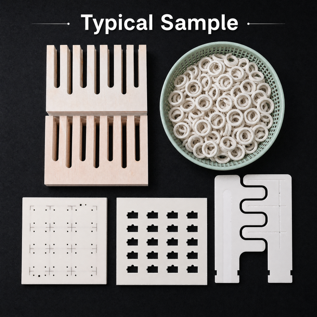
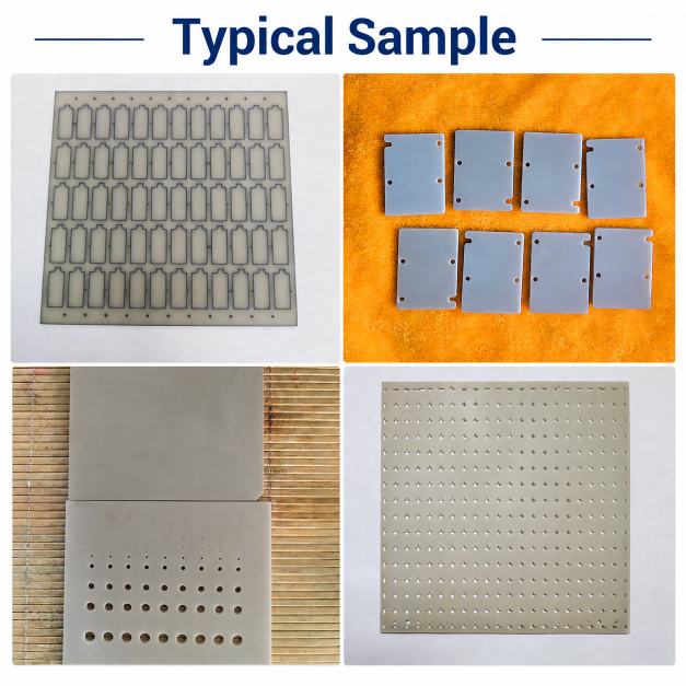
Alumina is the workhorse material for consumer device substrates and insulating parts. Mass singulation of multi-up alumina panels, cutting of thin alumina rings and forming of sensor housings all fall within the ceramic cutting category, with CCD alignment used where the pattern must register to printed features. Thin stock down to 0.05 mm is supported in the processing service, and vacuum fixturing keeps those sheets flat during cutting.
Automotive electronics: AlN power modules and motor-related parts
Under automotive duty cycles, aluminum nitride substrates carry heat away from power devices while isolating them electrically, and silicon nitride is used where mechanical toughness matters alongside thermal performance. Both are hard, brittle and expensive per sheet, which puts a premium on narrow kerf and on nesting efficiency. Drilling and contouring on the same platform avoids re-registration between the hole pattern and the outline.
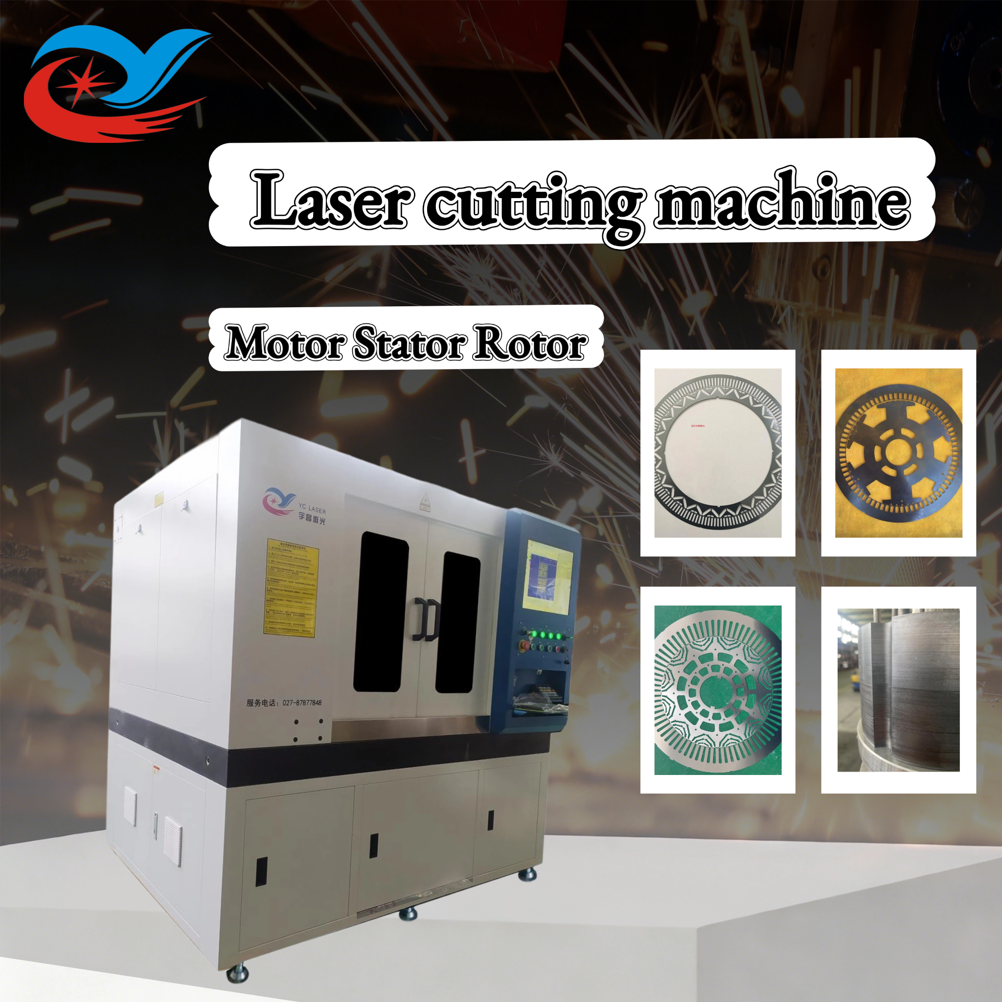
On the motor side, the platform includes a dedicated motor silicon steel sheet category (YC-GJM01). Industry technical reviews report that laser processing of silicon steel sheets reduces the heat-affected zone to below 0.1 mm, limiting magnetic performance degradation compared with mechanical punching — the reason laser routes are increasingly evaluated for laminated motor cores rather than only for prototype work.
PCB and packaging substrates
The boundary between ceramics and circuit substrates is thin in practice: HTCC and LTCC ceramics, metallized ceramics, copper-clad laminate and PCB substrates often run on the same line. The PCB precision laser cutting category (YC-GJMPCB) covers substrate depaneling and precision contouring, while the ceramic categories handle the fired ceramic work. For a plant producing both, this shared platform is the practical argument for one equipment family rather than two separate process chains.
Piezoelectric and specialty ceramics
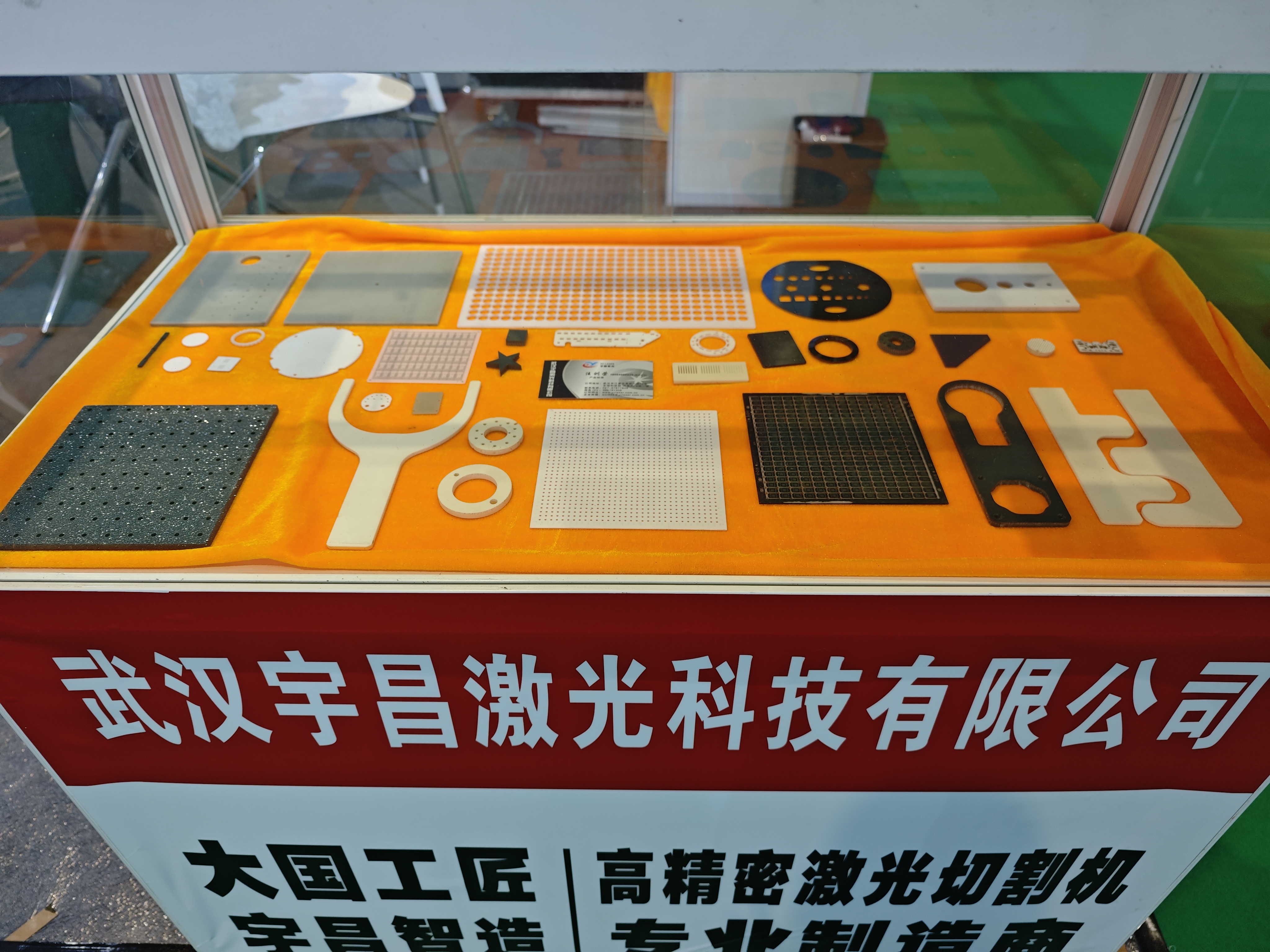
PZT and other piezoelectric ceramics are dimensionally sensitive: mechanical stress during separation shifts the electrical response of the element. Non-contact laser separation, with low micro-crack formation and minimal heat-affected zone, is the reason this material family is processed on the same platform. Ferrites, NdFeB magnets, sapphire, quartz and glass complete the material list, so a plant handling a mixed specialty-ceramic portfolio does not need a separate process for each material.
Configuration Fit at a Glance
The table below matches common electronics-ceramic operations to platform designations. Values are taken from the published machine and processing specifications; the correct configuration still depends on the specific part geometry and lot size.
| Operation | Typical part | Platform designation or category | Specified capability |
|---|---|---|---|
| Substrate singulation | Alumina and AlN substrates | YC-TC01 ceramic laser cutting machine | Cut thickness 0.01–20 mm; kerf 0.02–0.15 mm |
| Small-format part cutting | Small substrates, rings, spacers | YC-TCSF small-area category | Working area from 200×200 mm |
| Micro-hole drilling | Ceramic seals, cooling holes | YC-GJMD high-precision drilling | Drilling precision down to 0.05 mm |
| PCB substrate contouring | PCB substrates, copper-clad laminate | YC-GJMPCB PCB precision cutting | PCB precision laser cutting category |
| Lamination cutting | Motor silicon steel sheet | YC-GJM01 silicon steel category | Industry reports HAZ below 0.1 mm versus punching |
| Automated volume line | High-volume ceramic parts | YC-TCAT automatic loading and unloading | Automatic load/unload integration |
| High-mix micro parts | Small ceramic components | YC-BLDW dual worktable | Alternating station processing |
| Fine-feature / transparent work | Hard and brittle, glass, sapphire | YC-UVP, YC-UVN, YC-BLSW, YC-BLD | 355 nm and other wavelengths; glass categories |
Sources: YCLASER machine and processing specifications. Kerf, positioning and thickness values refer to the processing-service specification of the same equipment family.
The second table isolates the substitution decision itself, since most buyers evaluating this equipment are comparing it against an existing mechanical route rather than against another laser.
| Decision factor | Mechanical cutting / dicing | Laser platform |
|---|---|---|
| Contact with the part | Blade or wheel loads the ceramic edge | Non-contact beam, no mechanical clamping force |
| New design changeover | New tooling and fixture per contour | DXF/DWG import, program change only |
| Edge condition | Chipping and micro-crack risk under load | Low micro-crack and low chipping, minimal heat-affected zone |
| Features per setup | Contour and holes usually separate operations | Cutting, drilling, scribing and grooving on one platform |
| Thin sheet handling | Fixture-dependent, risk of distortion | Vacuum adsorption platform; cut thickness from 0.01 mm |
| Consumables | Blades, wheels, dressing tools | Beam source, optics and assist gas; no tool wear |
FAQ
What electrical and safety configuration does an exported ceramic laser cutting machine need?
Export configurations are built to meet the electrical standards of the destination region and ship with an English operating interface. The machine body is enclosed in a laser safety protection chamber to prevent beam leakage during operation. Installation conditions matter as much as the electrical package: ambient temperature of 5–35 °C, humidity of 40–65% RH without condensation, a dust-controlled or near-cleanroom area, a stable regulated industrial power supply and a vibration-damping foundation. Fume extraction is required because ceramic and glass processing produces fine dust that must be removed at the source.
Can one machine cut, dice, drill and scribe different ceramics?
Yes, within a configured range. The platform covers cutting thickness from 0.01 mm to 20 mm and drilling precision down to 0.05 mm, with CCD vision automatic positioning for cutting, drilling and scribing of ceramics, substrates and glass. YCLASER holds a utility model patent for an integrated machine for laser cutting, drilling and scribing of electronic ceramics with easy positioning. Material coverage includes zirconium oxide, aluminum oxide, aluminum nitride, silicon nitride, silicon carbide, metallized ceramics, PCB substrates, sapphire, glass, quartz, ferrites, NdFeB and wafer. Because power spans 10 W to 3000 W and wavelengths include 1060–1080 nm, 532 nm, 1064 nm, 355 nm and 10.6 µm, the actual boundary is set by the chosen source, not by the platform concept.
How should a buyer compare in-house equipment against outsourced ceramic processing?
Outsourced processing is charged on an hourly basis at 20–30 USD per hour with no minimum order quantity, which makes it the low-risk route for prototype and small-batch validation. In-house equipment becomes the better economic case when volume is continuous, when drawings are confidential, or when turnaround time on design iterations is the bottleneck. Machine cost itself varies with working area (200×200 mm to 1300×1300 mm), laser power and wavelength, so there is no single figure that applies across configurations; the practical approach is to fix the part family first and price the configuration that covers it.
Can our own ceramic parts be tested before a purchase decision?
Yes. YCLASER operates a process lab and a contract processing centre that support sample, small-batch and mass production work, with fast sample turnaround and acceptance of custom-specified processing requirements. New material verification produces qualified samples plus the process parameters intended for subsequent mass production, so the sample doubles as a production reference. An in-house process R&D team of eight engineers supports prototyping and non-standard customisation, and finished samples can be shipped by courier, land transport or sea freight.
What determines delivery time and ramp-up support?
Two factors dominate. The first is supply chain position: YCLASER is located in the Optics Valley laser industry cluster, with a complete local supply chain supporting fast delivery and rapid spare parts response, and a 2,000 m² manufacturing facility with annual production capacity of 100 units. The second is the service scope included with the machine: process consultation and parameter debugging before shipment, installation and operation training on site, and maintenance plus technical upgrades afterwards, delivered as one-to-one support. Export business accounts for 30% of sales, with Southeast Asia, Europe and the Middle East as the main markets.
Conclusion: Match the Configuration to the Ceramic, Not to the Brochure
For consumer and automotive electronics ceramics, the decision reduces to four checks. Confirm the operation mix — cutting, dicing, scribing, drilling or forming — because mixed-feature parts justify an integrated platform while single-feature volume does not. Confirm the material and thickness against the specified range, remembering that the processing service supports 0.05–11 mm with ≤6 mm stable mass production while the machine specification reaches 0.01–20 mm. Confirm the beam source against material absorption rather than against headline power. And confirm the fixture and inspection loop, since edge chipping at micron level is won or lost in fixturing and parameter control, not in axis speed alone.
Where the process replaces mechanical cutting, the gains are structural: no tool wear, no per-design tooling, no mechanical load on a brittle part, and changeover by drawing rather than by hardware. Where it replaces nothing and simply adds capacity for micro-ceramic parts, the dual-station and automatic loading configurations are what keep high-mix work economic.
Send a Drawing, Get a Process Answer
Share your ceramic part geometry, material and target batch size, and the YCLASER process team will confirm the matching configuration and return a cut sample with measured edge quality. Sample and small-batch processing is available with no minimum order quantity.
Email: wxr888@yclaser.com.cn | Tel / WhatsApp: +86 18602711568 | Website: www.whyc-laser.com
Download the full equipment catalogue: YCLASER CATALOG (PDF)
Wuhan Yuchang Laser Technology Co., Ltd. · 1st Floor, Building B, Phoenix Park, No.8, Optics Valley Science and Technology Park, No.18, Gaoxin 6th Road, Jiangxia District, Wuhan City
Have Questions or Need More Details?
Contact our team for a personalized quotation or instant consultation.
Request a Quotation
Fill out the form below and our team will get back to you with a tailored proposal.
WhatsApp Direct Chat
Prefer to chat in real-time? Message us on WhatsApp for instant assistance & quick answers.
- Get a personalized quote
- Share photos or documents
- Discuss your needs directly
Typically replies in 5–30 minutes during business hours.