Semiconductor Ceramic R&D Laser Cutting: Fixing No-MOQ, Compliance, and Delivery Friction
Semiconductor Ceramic R&D Laser Cutting: Fixing No-MOQ, Compliance, and Delivery Friction
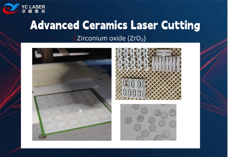
A semiconductor ceramic R&D program rarely needs volume. It needs twenty to forty parts across four or five designs, in zirconium oxide, aluminum oxide and aluminum nitride, cut to a tolerance the packaging team can inspect — and it needs them before the design freeze. That combination is where conventional ceramic cutting quotations break down: minimum order quantities set in the hundreds, multi-week queues, and no compliance paperwork to hand an EU customer for a twenty-part trial.
YCLASER — Wuhan Yuchang Laser Technology Co., Ltd., a laser equipment and laser processing company established in 2017 in Wuhan's East Lake High-tech Development Zone — answers that problem with a service rather than a machine purchase. Its laser processing service, service model designation Custom-laser-service-01, is performed on laser cutting machines holding ATTESTATION OF COMPLIANCE TTC-24-2012/02/01, is offered with no minimum order quantity, and covers zirconium oxide, aluminum oxide and aluminum nitride among its processed materials, at a positioning accuracy of ±0.005 mm and a kerf width of 0.02–0.15 mm.
The three blockers, answered in one paragraph: no minimum order quantity removes the volume gate; ATTESTATION OF COMPLIANCE TTC-24-2012/02/01, issued by Integra96 for the EU market and valid from 2024-12-20 to 2029-12-19, removes the documentation gate; and sample making quoted at 1–3 business days removes the scheduling gate.
What follows is a working guide for research engineers and procurement staff: what the service covers, how the compliance chain actually reads, the acceptance criteria to write into the order, why delivery dates slip, which machine risks to verify before a run starts, and when fully automated loading is worth paying for instead of manual loading.
Problem Definition: Why Small Ceramic R&D Lots Get Stuck
The obstacles in ceramic R&D procurement are rarely technical. Cutting a 0.8 mm zirconia coupon or a 2.5 mm aluminum nitride substrate is a solved process. The friction sits in three commercial and documentary gates that decide whether a prototype ships this month or next quarter.
Blocker 1 — The minimum order quantity
A shop that sets an MOQ of several hundred pieces is pricing setup time, not parts. For a lot of twenty coupons, an MOQ forces the buyer to over-purchase material for a design that may change at the next iteration, and it turns a process experiment into a capital commitment. The YCLASER service term is explicit: no minimum order quantity, with support for sample, small-batch and mass production.
Blocker 2 — Compliance evidence for an EU customer
An EU-facing OEM does not accept "the machine is CE-marked" as a statement. It wants a document with a number, an issuing body, a scope and a validity window. In this case the document is ATTESTATION OF COMPLIANCE TTC-24-2012/02/01, issued by Integra96, scoped to Laser Cutting Machines for the EU market, issued on 2024-12-20 and valid until 2029-12-19. That is a machine-level attestation, not a part-level certificate — a distinction worth stating plainly in any supplier questionnaire.
Blocker 3 — Delivery timing against an iteration cycle
If a ceramic redesign is validated every two weeks, a four-week queue consumes two iterations. YCLASER quotes sample making at 1–3 business days, which is what allows a research team to run a design change, inspect the coupon, and re-cut inside the same sprint. The rest of the timeline — 30 business days for standard models, 35–50 business days for non-standard customized models — applies to equipment, not to a service lot.
Industry Background: Small Volumes, Fast Iteration
Ceramic substrates, ceramic packaging bases, HTCC/LTCC ceramics and wafers sit at the front of the semiconductor supply chain, where the number of parts per design is small and the number of design revisions is high. Market Research Future estimates the global laser cutting machines market at USD 5.74 billion in 2024, projected to reach USD 12.61 billion by 2035 — a forecast shaped by exactly this kind of precision micro-processing demand rather than by sheet-metal throughput alone.
The technology mix matters for ceramics. Ultrashort-pulse sources are the reason brittle materials can be shaped without the thermal damage that mechanical or long-pulse routes introduce. Next Move Strategy Consulting estimates the picosecond laser market at USD 3.99 billion in 2026, growing at a 23.8% CAGR to USD 31.44 billion by 2035. YCLASER's own platform reflects that split directly: the precision laser cutting machine line includes the YC-UVP Ultraviolet Picosecond Laser Cutting Machine and the YC-UVN UV Nanosecond Laser Cutting Machine, and the company's semiconductor research case record describes cold processing that avoids thermal stress cracking and surface damage, with processing tolerance held at the micron level.
The practical consequence for a research buyer is that the process knowledge, not the machine ownership, is the scarce element. A supplier who has already characterised zirconia, alumina and aluminum nitride behaves differently on the first sample than a supplier learning the material on your order.
Detailed Solution: A No-MOQ Service Running on Certified Equipment
The service envelope, stated as specifications
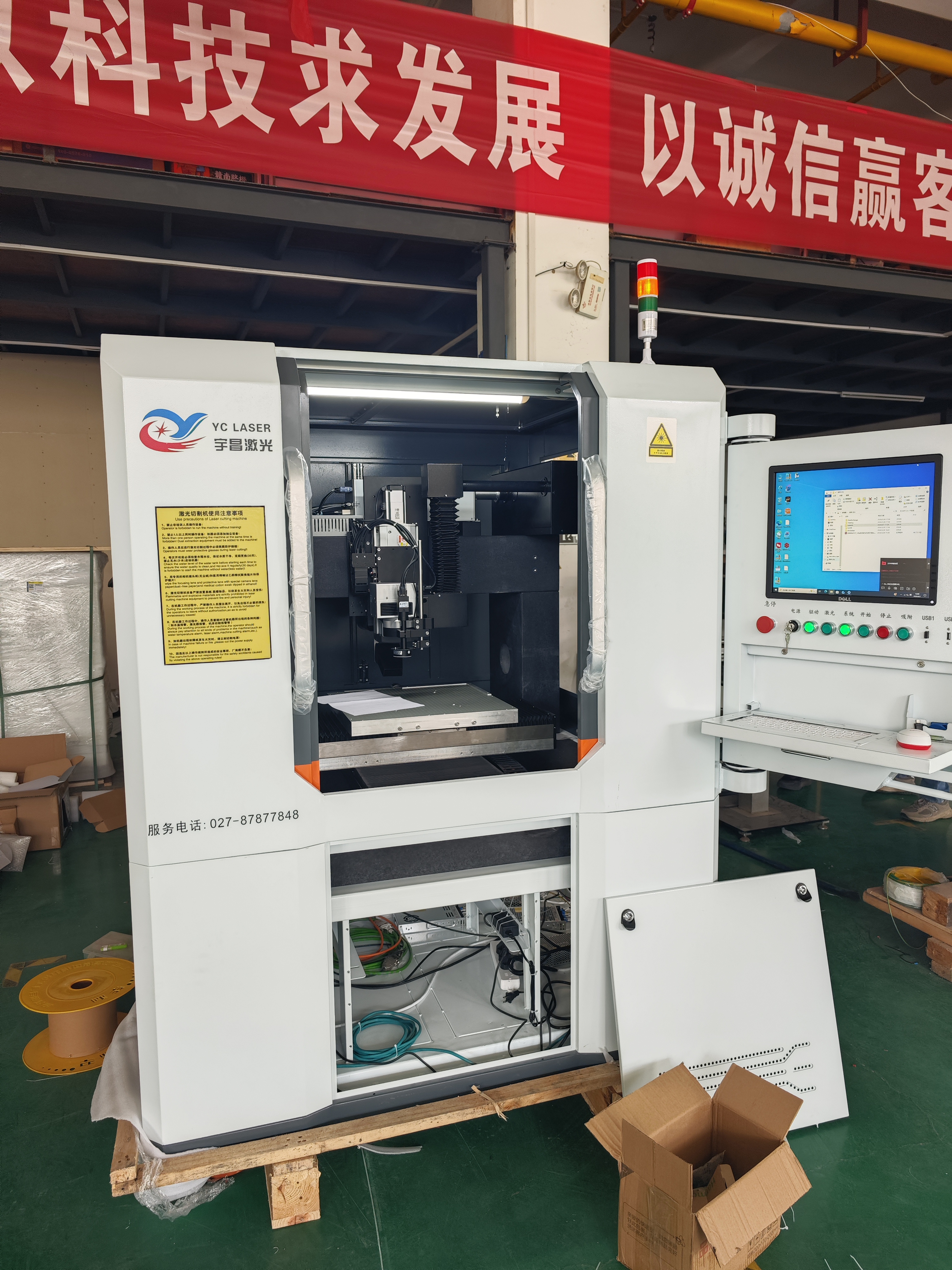
Custom-laser-service-01 is a precision ceramic laser cutting, laser ablation and micro-processing service. Its published parameters are the ones a design engineer should check first:
- Supported material thickness: 0.05–11 mm; stable mass-production thickness ≤6 mm.
- Positioning accuracy: ±0.005 mm.
- Kerf width: 0.02–0.15 mm.
- Charging: hour-based at 20–30 USD per hour.
- Order size: no minimum order quantity; sample, small-batch and mass production supported.
- Process character: high-precision non-contact laser processing with low micro-crack and low chipping results.
- Logistics: courier, land transport or sea freight.
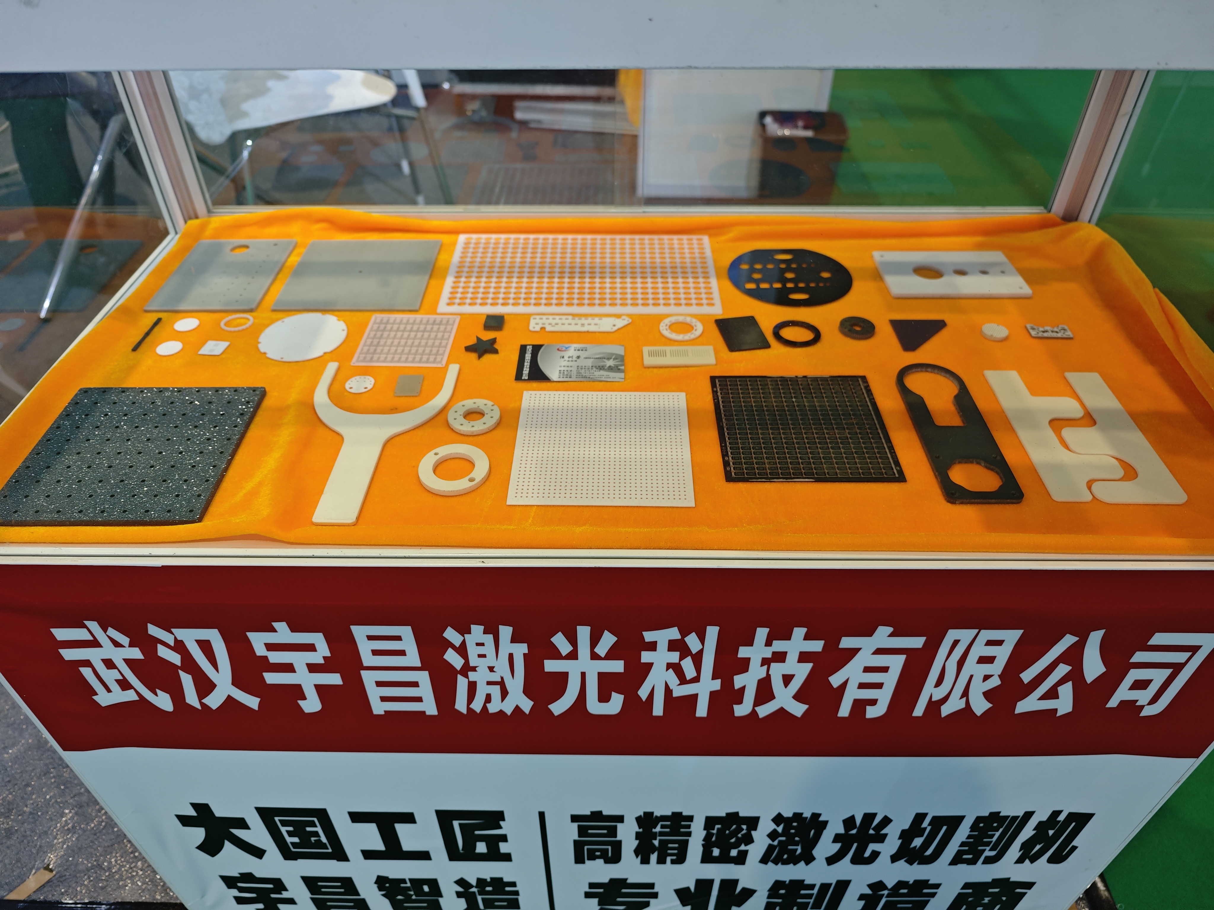
Processed materials include alumina ceramics, aluminum nitride (AlN), silicon carbide (SiC), silicon nitride, glass, ferrite, semiconductor-related materials, metals and PCB substrates. For a semiconductor ceramic R&D program the three materials that appear most often are zirconium oxide, aluminum oxide and aluminum nitride — all inside the stated scope.
The compliance chain, read precisely
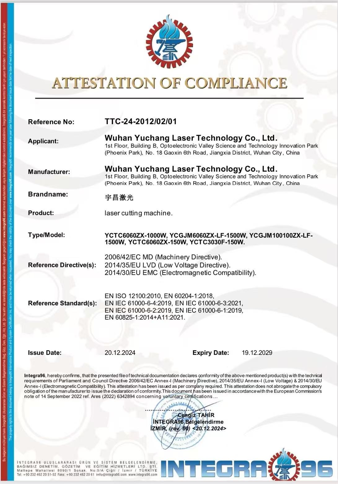
The attestation is the part of the offer most often summarised badly, so it is worth quoting in full. ATTESTATION OF COMPLIANCE TTC-24-2012/02/01 is issued by Integra96, applies to the EU market, and covers the scope Laser Cutting Machines. Its listed standards are:
- EN ISO 12100:2010
- EN 60204-1:2018
- EN IEC 61000-6-4:2019
- EN IEC 61000-6-3:2021
- EN IEC 61000-6-2:2019
- EN IEC 61000-6-1:2019
- EN 60825-1:2014+A11:2021
The covered Precision laser cutting machine models are YC-TC01, YC-TCSF, YC-TCHP, YC-TCAT, YC-GJMD, YC-GJMPCB, YC-GJM01, YC-BLD, YC-BLSW, YC-BLDW, YC-UVP and YC-UVN. The covered configurations include ceramic, small-area, high-power, fully automatic loading and unloading, high-precision drilling, PCB and motor silicon steel sheet laser cutting machines.
Two limits should be stated honestly. First, the attestation covers the machines — the service is performed on machines holding TTC-24-2012/02/01, but it does not certify the ceramic part itself. Second, it is an EU-market document; separate Chinese registrations exist in the same portfolio, including Chinese Utility Model Patent ZL 2020 2 2568710.8 issued by the State Intellectual Property Office, and Computer Software Copyright Registration No. 2020SR1720714 (Certificate No. 6521686) for the High-Precision Laser Cutting System V1.0, issued 2020-12-03 by the National Copyright Administration of the People's Republic of China and valid until 2070-07-18. Those are different instruments for a different purpose and should not be presented as EU compliance.
What "no MOQ" actually changes
Removing the MOQ converts a purchasing decision into an experimentation loop. A team can send one drawing, receive a coupon, measure the kerf and the chipping, adjust the feature size, and resend — with each round billed on process hours at 20–30 USD per hour rather than on a fixed batch of parts. The cost driver shifts from "how many pieces must I commit to" to "how many process hours does this geometry consume", which is a far more useful number during feasibility work.
Step-by-Step Breakdown: From Drawing to Accepted Parts
- Send the drawing and the material callout. The service runs on equipment compatible with DXF/DWG drawings and intelligent nesting optimisation, so a native CAD file removes the interpretation step that causes most first-round errors. State the material (for example zirconium oxide, aluminum oxide or aluminum nitride) and the nominal thickness.
- Agree the process route. Different feature sets map to different operations: contour cutting, micro-hole drilling, grooving or dicing. YCLASER holds a Chinese Utility Model Patent (ZL 2020 2 2568701.9, issued 2021-07-06) for an integrated machine for laser cutting, drilling and scribing of electronic ceramics with precise positioning — useful context when a single part requires more than one operation.
- Run the sample. Sample making is quoted at 1–3 business days. This is the step where edge quality, kerf and hole diameter are confirmed on your material rather than on a reference material.
- Freeze the acceptance criteria in writing. Do this before the batch is released, not after (see the next section for the specific numbers to use).
- Release the batch. Because there is no minimum order quantity, a lot can be ten pieces or several thousand; charging remains hour-based at 20–30 USD per hour.
- Choose the logistics mode and receive the documentation. Courier, land transport and sea freight are all available; the mode should be selected at order confirmation, not at shipment.
Acceptance Criteria to Write Into a Ceramic R&D Order
Vague acceptance language is the most common source of rework in ceramic prototyping. The criteria below are drawn from the service's published capability and should appear in the purchase documentation.
- Dimensional tolerance: the platform holds ±0.005 mm positioning accuracy, so specify the contour tolerance you actually need rather than "as precise as possible".
- Hole size: drilling precision is quoted at a minimum of 0.05 mm; features below that threshold are a different process discussion.
- Kerf: 0.02–0.15 mm. State which end of the range your design assumes, because kerf compensation changes the programmed contour.
- Edge quality: the service is characterised by low micro-crack and low chipping results. R&D specifications typically call for edge chipping controlled at the micron level, so define the inspection method alongside the limit.
- Thickness: 0.05–11 mm is supported, with ≤6 mm as the stable mass-production range. A 9 mm trial coupon is a process discussion, not a catalogue line item.
- Inspection equipment: the process setup references metallurgical microscope, aperture measuring instrument and 2D measuring instrument as the external inspection accessories used to check dimensions and edge quality — naming the instrument removes ambiguity about how a result will be judged.
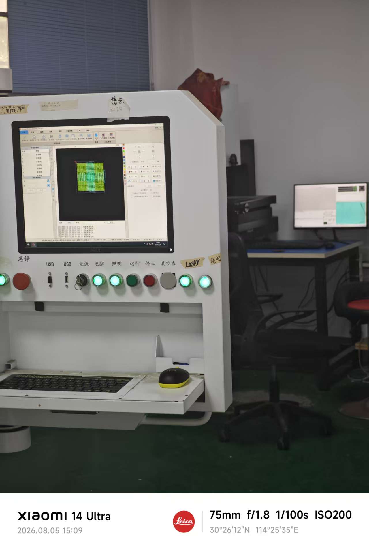
Machine-build quality control is a separate layer and follows a defined sequence: optical path accuracy calibration, repeatability testing, whole-machine power-on aging test, actual material trial cutting verification, full-function program testing, and issuance of a factory quality inspection report. When a research team plans to transfer a process to a production machine later, that sequence is the evidence to request.
Why Delivery Dates Slip — and How to Prevent It
Delivery failures in ceramic R&D processing follow a predictable pattern. None of the causes below require new data to explain; they follow from the process constraints already stated.
- Drawing data that cannot be nested. If the file arrives as a PDF rather than DXF/DWG, the nesting and toolpath step becomes manual. Send native geometry.
- Material that has not been characterised. A new ceramic grade needs parameter development; YCLASER's support scope explicitly includes process debugging for unfamiliar materials. Budget that step into the plan for a first-time material.
- Fixturing for thin or large parts. Thin wafers and large plates require tooling, fixtures or a vacuum adsorption platform. A 0.8 mm coupon and a 3 mm plate do not present the same handling problem.
- Acceptance criteria that arrive late. A tolerance agreed after the batch is cut turns a delivery into a rework loop.
- Logistics decided at the end. Courier, land transport and sea freight have very different transit profiles; the choice should be made when the order is confirmed.
- Confusing a service lot with an equipment order. Equipment lead time is 30 business days for standard models and 35–50 business days for non-standard customized models; OEM/ODM bulk orders are quoted at 3–10 business days depending on process complexity and order volume. A service lot should be planned against sample turnaround, not against machine build time.
Malfunction Risk Checks Before a Run Starts
For a research buyer, machine risk is usually invisible until it becomes a schedule risk. Six checks cover most of it, and every one of them is a question that can be asked during supplier qualification.
- Thermal stability: an industrial chiller cools the laser to keep output stable. Without it, kerf and edge quality drift through the shift.
- Dust and fume extraction: ceramic and glass processing generates dust that contaminates optical lenses; an extraction system is part of the standard equipment set.
- Power quality: a stable industrial voltage regulator is specified precisely to avoid voltage fluctuation effects.
- Environment: ambient temperature 5–35 °C, humidity 40–65% RH without condensation, clean or near-cleanroom dust control, and a vibration-damping foundation for accuracy.
- Laser safety: an enclosed laser safety protection chamber prevents leakage — the same requirement that sits behind EN 60825-1:2014+A11:2021 in the attestation.
- Spares and response: YCLASER maintains a stock of original parts for rapid replacement and provides 24/7 remote technical support covering troubleshooting, software debugging and process parameter optimisation, with paid on-site installation and maintenance available overseas.
Fully Automated vs Manual Loading for R&D Volumes
The loading decision is a volume decision, not a precision decision. YCLASER equipment supports four operating modes: automatic mode, where DXF/DWG drawings are imported, nesting runs automatically and processing continues unattended; manual debugging mode for single-point marking, partial test cutting, parameter debugging and sample testing; semi-automatic mode, where the operator loads and unloads while the machine executes the program; and integration with automated production lines for automatic loading and unloading, available as an option. The fully automatic loading and unloading configuration is covered by the same attestation, under the YC-TCAT designation among the covered models.
| Decision factor | Manual / semi-automatic loading | Fully automatic loading and unloading |
|---|---|---|
| Typical fit | High-mix R&D lots, frequent design changes, parameter trials | Continuous runs of a stable design, production-line integration |
| Changeover | Operator handles each new design directly | Programme change; mechanical setup is fixed |
| Labour model | Operator present per cycle | Unattended continuous processing |
| Where it is documented | Manual debugging and semi-automatic modes | Optional automatic loading and unloading integration; YC-TCAT configuration |
| Compliance status | Covered configurations under TTC-24-2012/02/01 | Covered configurations under TTC-24-2012/02/01 |
For an R&D program the practical rule is simple: manual or semi-automatic loading until the design stops changing, then evaluate automation against a measured cycle. Automation is not a substitute for a characterised process — it multiplies whatever the process already does.
Use Cases: Where This Configuration Has Already Run
Deployment records are the most useful part of a capability claim, because they describe conditions rather than intentions.
- National-level semiconductor materials research institute (China). A custom-designed semiconductor-specific ceramic laser cutting machine supports micro/nano cutting, precision drilling and grooving of ceramic substrates, ceramic packaging bases and high-frequency ceramic components. After 2+ years of stable operation, the record notes cold processing that avoids thermal stress cracking and surface damage, with tolerance held at the micron level, serving R&D and small-batch prototyping.
- University research platform, Tsinghua University (China). A small-format ceramic laser cutting system entered a laboratory public testing and pilot-scale platform, where it has run for 3+ years on precision cutting, micro-hole drilling and irregular dicing of advanced functional and structural ceramics.
- High-end electronic component manufacturer (Taiwan). A dual-head, dual-beam-path ceramic laser cutting machine supports simultaneous dual-station processing, with independent or synchronous switching between beam paths. After 2+ years, the recorded result is consistent accuracy at both stations with no cumulative deviation, serving multi-product, small-batch flexible production.
- High-precision manufacturing company (South Korea). One high-configuration machine was exported for ultra-precision cutting and micro-hole processing of precision ceramic parts, with 1.5+ years of stable overseas operation.
These deployments describe equipment, while the service is delivered on the same process platform — which is the point: the parameters that shaped those results are the parameters applied to a service lot. For a program with a different requirement set, YCLASER holds an in-house process R&D team of 8 engineers, operates a 2,000 m² facility with annual output of 100 units, and exports about 30% of output to Southeast Asia, Europe and the Middle East.
Comparison Table: Zirconium Oxide, Aluminum Oxide, Aluminum Nitride
All three materials are inside the service scope. What differs is the sample evidence on file and the detail that must be settled at intake.
| Material | In service material scope | Documented sample thicknesses | Confirm at intake |
|---|---|---|---|
| Zirconium oxide | Yes — listed among processed materials | 0.82 mm, 2 mm, 3 mm | Handling method for sub-1 mm coupons; edge chipping limit defined against the inspection instrument |
| Aluminum oxide | Yes — listed among processed materials | 0.3 mm, 2 mm, 2.3 mm, 2.5 mm, 3 mm | Kerf assumption within the 0.02–0.15 mm range; whether contour and holes run in one operation |
| Aluminum nitride (AlN) | Yes — listed among processed materials | 2.5 mm, 3 mm | Hole diameter versus the 0.05 mm minimum drilling precision; thickness against the ≤6 mm stable production range |
Service envelope applying to all three materials: thickness 0.05–11 mm, stable mass production ≤6 mm; positioning accuracy ±0.005 mm; kerf 0.02–0.15 mm; hour-based charging 20–30 USD/h; no minimum order quantity.
FAQ
Is the laser processing service performed on EU-compliant equipment?
Yes. Laser processing services are performed on laser cutting machines holding ATTESTATION OF COMPLIANCE TTC-24-2012/02/01, issued by Integra96 for the EU market on 2024-12-20 and valid until 2029-12-19, with the scope stated as laser cutting machines. The attestation references EN ISO 12100:2010, EN 60204-1:2018, EN IEC 61000-6-4:2019, EN IEC 61000-6-3:2021, EN IEC 61000-6-2:2019, EN IEC 61000-6-1:2019 and EN 60825-1:2014+A11:2021, and covers models YC-TC01, YC-TCSF, YC-TCHP, YC-TCAT, YC-GJMD, YC-GJMPCB, YC-GJM01, YC-BLD, YC-BLSW, YC-BLDW, YC-UVP and YC-UVN. It is a machine-level document, not a certificate for the processed part.
Which ceramic materials can be processed, and at what accuracy?
Processed materials include alumina ceramics, aluminum nitride (AlN), silicon carbide (SiC), silicon nitride, glass, ferrite, semiconductor-related materials, metals and PCB substrates; zirconium oxide is also processed. Positioning accuracy is ±0.005 mm and kerf width is 0.02–0.15 mm. Supported material thickness is 0.05–11 mm, with ≤6 mm treated as the stable mass-production range, and drilling precision is quoted at a minimum of 0.05 mm. Results are described as low micro-crack and low chipping, achieved through high-precision non-contact laser processing.
How is a small R&D lot priced if there is no minimum order quantity?
Charging is hour-based at 20–30 USD per hour. Because there is no minimum order quantity, a lot is priced by process time rather than by a fixed batch size, and sample, small-batch and mass production are all supported under the same model. In practice this means the quotation follows the geometry and the number of operations — contour cutting, drilling or grooving — rather than the piece count alone.
Can we validate with a sample before releasing a batch?
Yes. Sample making is quoted at 1–3 business days, and the service is explicitly structured to support sample, small-batch and mass production with no minimum order quantity. A sample run is the stage where kerf, edge chipping and hole diameter are confirmed on your own material, and where acceptance criteria should be fixed in writing before the batch is released. Multiple logistics options — courier, land transport and sea freight — apply to sample shipments as well as to production lots.
What lead time should be planned, and can loading be automated?
Sample making is 1–3 business days. Equipment lead time is 30 business days for standard models and 35–50 business days for non-standard customized models, while OEM/ODM bulk orders are quoted at 3–10 business days depending on process complexity and order volume. On loading, both paths exist: manual debugging and semi-automatic modes for high-mix R&D work, and fully automatic loading and unloading for continuous runs, available as an option and covered by the same attestation. To size either path against your own part mix, send a drawing and a material callout for a process review — contact YCLASER at whyc-laser.com or by email at wxr888@yclaser.com.cn.
Conclusion
For semiconductor ceramic R&D, the binding constraints are commercial and documentary long before they are technical. A minimum order quantity decides whether an experiment is affordable; a named compliance instrument decides whether an EU customer can accept the part; a sample turnaround of 1–3 business days decides whether a design iteration fits inside the project schedule. All three are addressed by a service model — Custom-laser-service-01 — that runs on machines holding ATTESTATION OF COMPLIANCE TTC-24-2012/02/01, processes zirconium oxide, aluminum oxide and aluminum nitride to ±0.005 mm positioning accuracy and 0.02–0.15 mm kerf, and carries no minimum order quantity.
The remaining work belongs to the buyer: send native DXF/DWG geometry, state the material and thickness against the 0.05–11 mm envelope, fix acceptance criteria before the batch, and choose manual or automated loading against a measured cycle rather than an assumed one. Done in that order, a twenty-part ceramic lot stops being a procurement exception and becomes a routine step in the development loop.
Start With One Drawing and One Sample
Send a ceramic part drawing with its material and thickness, and YCLASER will confirm the process route, the achievable kerf and the sample date — no minimum order quantity, and no commitment beyond the sample itself.
Email: wxr888@yclaser.com.cn | Tel / WhatsApp: +86 18602711568 | Web: www.whyc-laser.com
Download the full equipment and service catalogue: YCLASER CATALOG (PDF)
Have Questions or Need More Details?
Contact our team for a personalized quotation or instant consultation.
Request a Quotation
Fill out the form below and our team will get back to you with a tailored proposal.
WhatsApp Direct Chat
Prefer to chat in real-time? Message us on WhatsApp for instant assistance & quick answers.
- Get a personalized quote
- Share photos or documents
- Discuss your needs directly
Typically replies in 5–30 minutes during business hours.