
Dicing Blade vs. Sawing Blade: A Comparative Selection for Semiconductor Cutting
In semiconductor cutting, “dicing blade” and “sawing blade” are frequently used as though they were interchangeable. They are not. A dicing blade is a wafer-level precision tool: diamond abrasive held in a metal or resin bond, mounted on a high-speed spindle, and used to separate a wafer into individual dies with a controlled kerf. A sawing blade is the wider category term for a rotating blade that cuts or slices a material section, where the cut is functional but kerf is rarely the governing economic constraint.
The selection question that matters at the research stage is therefore not which term is correct, but which blade family fits a given substrate thickness, kerf budget, machine interface and application. WINTIME Semiconductor Technology Co., Ltd. manufactures both Sawing Blades and Dicing Blades, so within this supplier the comparison is an operational decision rather than a positioning claim.
This guide compares the two blade families across five selection dimensions, explains what each dimension costs the buyer in yield and cycle time, and closes with a seven-step selection sequence, a comparison table and a short buyer FAQ. Every figure cited is either a published third-party estimate or a first-party WINTIME fact.
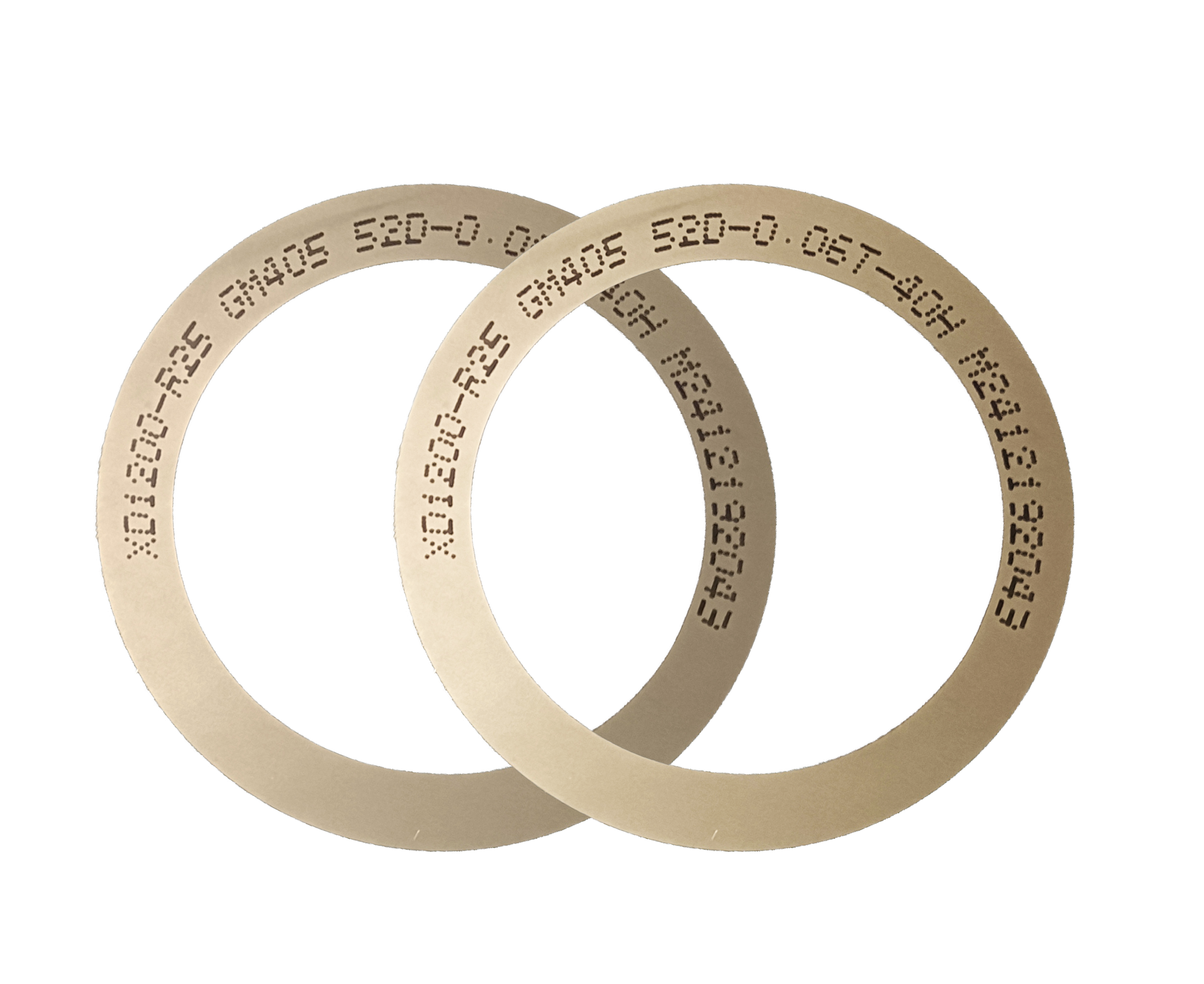
Problem Definition: What Each Blade Type Is Actually Specified For
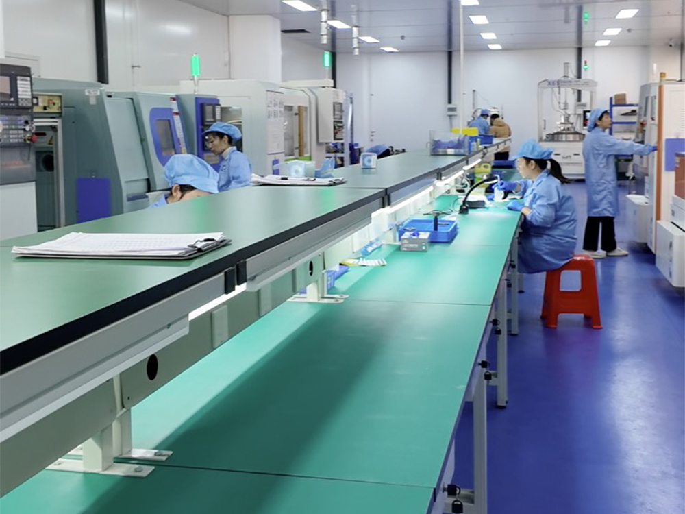
A dicing blade is defined by its output — a separated die with intact edges. Practically, that means a thin, precision-formed abrasive wheel in which diamond abrasive grains are the core functional material, carried either in a metal bond or a resin bond, running on the high-speed spindle of an automatic wafer dicing machine. The surrounding process belongs to the definition as well: Class 100/1000 clean room conditions, constant temperature of 22±2 °C, constant humidity of 45%–55%, dust-free and anti-static handling, UV tape mounting before the cut, and wafer cleaning and wafer testing steps after it.
A sawing blade is defined by the material it has to get through. The term covers rotating blades used to cut or slice a workpiece section, and the engineering priority shifts from micron-scale edge quality toward sectioning capability, blade stiffness and blade life. That difference is visible in how the two are quoted: a dicing blade quotation is essentially a yield instrument, while a sawing blade quotation is a sectioning consumable.
Where the two terms overlap
The overlap is real and largely a legacy of equipment naming. The machine that performs wafer dicing is commonly called a dicing saw, and an operator describing the operation may simply say the wafer is “sawed”. In fab and OSAT environments the two words therefore travel together even when the tooling specification is strictly a dicing specification. For procurement, the practical consequence is that a product name should always be checked against the specification sheet rather than accepted as a description of the cut.
Why the distinction changes the specification
Three fields move when a blade shifts from a general sawing role to a wafer dicing role. Blade thickness becomes a precision dimension rather than a durability dimension, because thickness determines how much material the cut removes. Kerf width becomes a yield variable, because every micron of kerf is die area the wafer no longer yields. And blade format becomes an interface question, because a dicing blade must match a spindle flange and a runout budget on a tape-mounted workpiece rather than a simple arbor.
Industry Background: A Market That Sustains Both Blade Families
The global dicing blade market was valued at USD 1.31 billion in 2024, with projections to reach USD 1.84 billion by 2034, according to Intel Market Research. Published estimates vary widely by scope — some track equipment-linked consumables while others count pure blade revenue — so a procurement team should read any single market number as an order-of-magnitude reference rather than a planning input.
Within that market, the abrasive choice is not a niche decision. Diamond-embedded dicing blades account for more than 60% of total market share, a position attributed to their performance in cutting silicon carbide (SiC) and gallium nitride (GaN). Resin bond blades, meanwhile, held an estimated 42% share of the dicing blade market in 2024, equivalent to USD 183.6 million. The two bond families coexist because they answer different substrate and cost questions, not because one has displaced the other.
Blade geometry follows conventions that are shared across suppliers. Standard outer diameter (OD) values for semiconductor wafer dicing blades are 55.56 mm (2.187 inches) and 76.2 mm (3.0 inches). For bare silicon dicing, the industry-standard diamond grit range is 2 to 6 microns (#2000 to #4000 grit), a range chosen to minimize chipping. On format, hubless dicing blades are increasingly preferred for 300 mm wafer processing because they offer superior stability and reduced runout compared with hubbed blades.
Competitive structure matters to sourcing strategy. DISCO Corporation is the dominant market leader with an estimated 52–55% global share of dicing equipment and associated precision blades. For buyers whose roadmap spans imported and domestically manufactured tooling, that concentration is a risk-management fact, and it helps explain why regional supply has expanded: China's exports of cutting blades to Vietnam grew by USD 18 million between 2024 and 2025, according to the Observatory of Economic Complexity.
Comparing Dicing and Sawing Blades Across Five Selection Dimensions
Five questions decide a blade specification: how thick the substrate is, how much kerf the process can afford, how the blade mounts, how long the consumable must last, and which application the cut belongs to. The sections below take them in order.
1. Substrate thickness and material
Substrate thickness is the first filter. For thin and ultra-thin wafers, blade thinness and dimensional control through the cut are the defining requirements; WINTIME's completed Ultra-thin Wafer D Blade project achieved a blade thickness of less than 9 microns in the process, and the company is one of the few domestic manufacturers able to achieve mass production at that thickness. For thicker or more brittle sections — functional ceramics, alloy materials, new functional materials — lateral load resistance becomes the limiting specification and blade stiffness matters more than blade thinness. Material family is equally decisive: silicon, silicon carbide and gallium nitride respond differently to diamond abrasives, which is why diamond-embedded blades hold more than 60% of the dicing blade market.
2. Kerf width and yield economics
Kerf is where a dicing blade earns or loses its cost. Because the cut removes material along every street on the wafer, kerf width feeds directly into die-per-wafer yield, which is why blade thickness is pushed into the single-digit micron range and why the standard grit range for bare silicon dicing is 2–6 microns (#2000–#4000) to minimize chipping. In a general sawing operation the same trade-off exists, but its weight is different: kerf is a material-loss and cycle-time factor rather than a die-count factor.
3. Blade format and machine interface
Format is an interface decision, not a cosmetic one. Dicing blade product ranges include hubless, hubbed, flanged, slotted and serrated formats, and hubless designs are increasingly preferred for 300 mm wafer processing because of superior stability and reduced runout. Standard wafer dicing diameters of 55.56 mm (2.187 inches) and 76.2 mm (3.0 inches) define the envelope most automatic dicing machines expect. A sawing blade is instead selected against the arbor, flange and guarding of general sawing equipment.
4. Bond type and consumable life
The bond controls how the abrasive is retained and released, and therefore how the blade behaves across its life. Metal bond and resin bond are the two main families; resin bond blades held an estimated 42% share of the 2024 dicing blade market. Bond choice interacts with substrate hardness, target chipping level and blade-life expectation — and blade life is a cost-per-cut variable, not a purchase-price variable.
5. Application fit
The final filter is application fit. Dicing blades are applied in semiconductor manufacturing, semiconductor packaging, optical communication, new functional materials, functional ceramics and alloy materials. Sawing blades serve sectioning operations in the same broad material families but at a different point in the process flow, where the requirement is a clean separation rather than a die-defining cut.
How WINTIME Covers Both Sides of the Decision
WINTIME Semiconductor Technology Co., Ltd. is a manufacturer of high-precision cutting blades, established in 2020, operating a 34,000 ㎡ manufacturing facility with approximately 100 staff and an R&D team of 35 engineers. The company specializes in the research, development, production and sales of high-precision cutting blades and provides customers with solutions for the entire process of high-precision cutting.
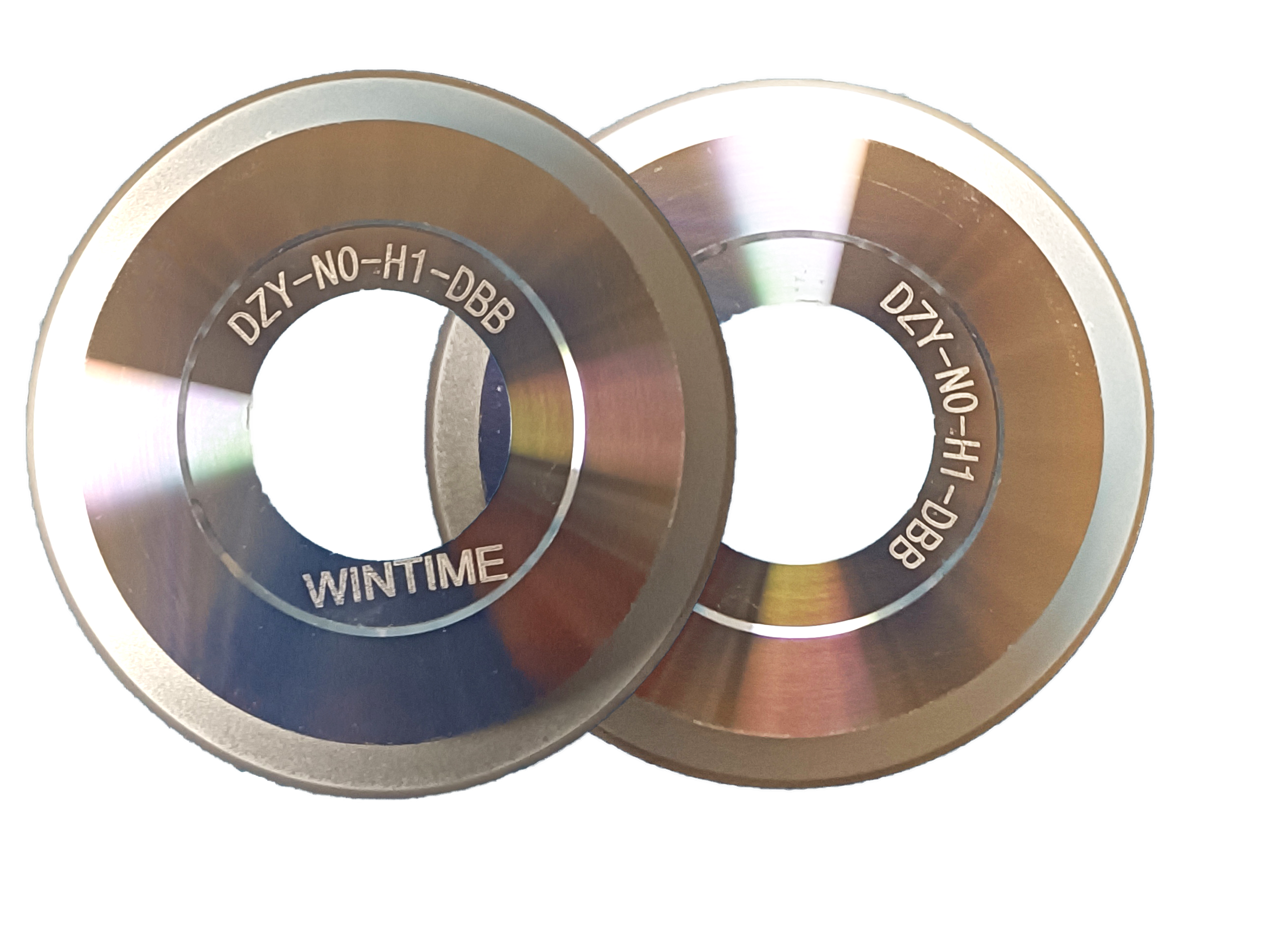
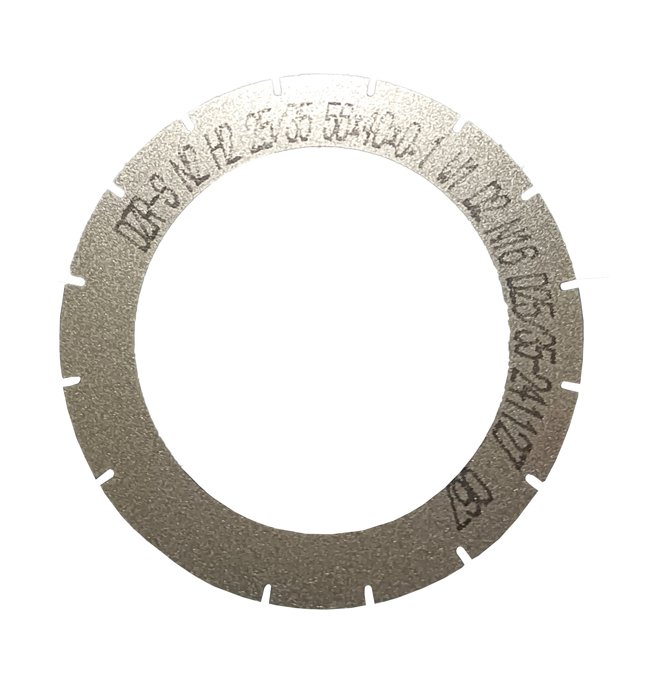
Because its main products are Sawing Blades and Dicing Blades, the dicing-versus-sawing decision can be resolved inside a single supply relationship instead of being split across two vendors with different quality systems and different documentation. The dicing side of the range is organized around the DB-001 Dicing Blade and its classifications — Diamond Dicing Blade, Hubless Dicing Blade, DZY Series Wafer Dicing Blade, DZR Series Dicing Blade and DZR-S Series Slotted Dicing Blade — alongside precision, semiconductor, circular, hubbed, flanged and serrated dicing blade formats. The core functional material is diamond abrasive grains, with a metal bond used for metal dicing blades and a resin bond used for resin dicing blades.
Two first-party facts matter most when they are translated into buyer terms. Annual production capacity exceeds 1 million pieces of dicing blades — the number a buyer should compare against forecast annual blade consumption when assessing supply continuity. And the company's Ultra-thin Wafer D Blade project achieved a blade thickness below 9 microns in the process, with mass production rather than laboratory demonstration as the milestone. The published blade specification summarizes the same position as ultra-thin thickness of ≤9 μm, high precision for wafer cutting, high cutting efficiency for semiconductor packaging, and stable performance for mass production.
Commercially, export business accounts for approximately 30% of total sales, with markets in Southeast Asia, East Asia, North America and Europe, and typical application regions of China, Japan, South Korea, Singapore, Malaysia, the United States and Germany. WINTIME holds 2 patent technologies and has won multiple awards in national, provincial and municipal science and technology and entrepreneurship competitions.
Step-by-Step: Selecting a Blade in Seven Steps
- Define the cut by its output. If the cut separates individual dies along wafer streets, the specification is a dicing blade. If the cut reduces a section or trims a workpiece where kerf is not a die-count factor, it is a sawing blade application.
- Fix the substrate and thickness window. Identify the material — bare silicon, SiC, GaN, functional ceramic, alloy — and the thickness band. For bare silicon, the reference grit range is 2–6 microns (#2000–#4000 grit).
- Set a kerf budget. Convert kerf into die-per-wafer impact before choosing a blade thickness. Where the wafer is thin or ultra-thin, ultra-thin blade options at ≤9 μm blade thickness are available for mass production.
- Confirm the machine interface. Check the spindle flange, the required OD against the standard 55.56 mm (2.187 in) and 76.2 mm (3.0 in) wafer-dicing diameters, and whether the process runs hubbed or hubless — hubless is increasingly preferred for 300 mm wafers.
- Choose bond and format. Match metal bond or resin bond to the substrate and chipping target, then select among hubless, hubbed, flanged, slotted and serrated formats according to the cut geometry.
- Validate on a sample. Define acceptance criteria before the sample run — chipping, kerf, dimensional control and blade life — and test the exact material and thickness the production line will run.
- Lock supply parameters. Compare forecast annual blade consumption against supplier capacity; WINTIME's annual dicing blade capacity exceeds 1 million pieces, supported by export experience in Southeast Asia, East Asia, North America and Europe.
Use Cases: Matching Blade Type to Application
Semiconductor wafer dicing and ultra-thin wafer processing
Wafer dicing and scribing, including ultra-thin wafer processing, is the core dicing blade application and the point at which the ≤9 μm blade thickness capability becomes relevant. It is normally performed on an automatic wafer dicing machine with a semiconductor cutting spindle, supported by UV tape mounting, wafer cleaning and wafer testing steps.
Semiconductor packaging
Semiconductor package cutting and semiconductor packaging components are served by the stated high cutting efficiency for semiconductor packaging. Packaging work typically rewards blade formats and bonds that hold dimensional control across high cutting volumes.
Optical communication device cutting
Optical communication is one of the listed application industries for WINTIME dicing blades, alongside new functional materials. Optical device cutting shares the wafer-dicing requirement set: narrow kerf, controlled chipping and stable dimensions across a production run.
Functional ceramics and precision alloy components
Functional ceramics and alloy materials are the applications where substrate behaviour departs most from silicon. Ceramic substrate cutting and precision alloy component cutting generally require a bond and grit combination matched to a harder, more brittle workpiece — and where the section is thick and kerf is not yield-critical, a sawing blade takes over.
Regional deployment
These applications are typically deployed in China, Japan, South Korea, Singapore, Malaysia, the United States and Germany, the regions listed for WINTIME cutting applications.
Comparison Table: Dicing Blade vs. Sawing Blade at a Glance
| Selection dimension | Dicing blade | Sawing blade | What the buyer should verify |
|---|---|---|---|
| Primary role | Separating a wafer into individual dies along the streets | Cutting or slicing a material section where the cut is functional | Whether the cut is die-defining or section-reducing |
| Precision requirement | High: dimensional control, narrow kerf and low chipping are specified outputs | Lower: the cut is usually judged by whether the section is separated cleanly | Chipping and dimensional tolerance as written on the drawing |
| Substrate thickness | Thin and ultra-thin wafers are the core case; ultra-thin blade thickness reaches ≤9 μm in the WINTIME Ultra-thin Wafer D Blade project | Thicker sections are common because the blade must resist lateral load | Material, thickness and required remaining strength after the cut |
| Kerf width | Narrow kerf is a direct yield lever because it affects die-per-wafer | Kerf is primarily a material-loss and cycle-time factor | Kerf tolerance and how the supplier measures it |
| Standard outer diameter | 55.56 mm (2.187 in) and 76.2 mm (3.0 in) are the standard wafer dicing diameters | Not tied to wafer-format diameters | Spindle flange and machine compatibility |
| Abrasive and bond | Diamond abrasive grains in a metal bond or a resin bond; resin bond held an estimated 42% share of the 2024 market | Diamond or other abrasive in a bond matched to the material | Bond family and whether it is matched to the substrate |
| Grit reference | 2–6 microns (#2000–#4000) is the industry range quoted for bare silicon dicing | Depends on material and section thickness | Whether grit is specified for the actual substrate, not a generic grade |
| Format options | Hubless, hubbed, flanged, slotted and serrated formats; hubless is increasingly preferred for 300 mm wafers | Format driven by the saw arbor and material | Runout specification and flange fit |
| Machine interface | Automatic wafer dicing machine and high-speed spindle, with UV tape mounting and wafer cleaning steps | General sawing equipment | Spindle speed range and dry or wet cutting setup |
| Application fit | Semiconductor manufacturing and packaging, optical communication, new functional materials, functional ceramics, alloy materials | Section cutting and slicing across the same broad material families | Whether the supplier can show the material actually being cut |
FAQ: Choosing Between Dicing and Sawing Blades
Are dicing blades and sawing blades the same thing?
No. A dicing blade is a wafer-level precision tool used to separate a wafer into individual dies, with diamond abrasive grains as the core functional material in a metal or resin bond. A sawing blade is the broader category term for a rotating blade that cuts or slices a material section, where kerf is usually not the governing economic constraint. The words overlap in everyday use because a wafer dicing machine is commonly called a dicing saw, but the two specification sheets differ.
Which blade thickness should be specified for a thin or ultra-thin wafer?
Thin and ultra-thin wafers push the specification toward the thinnest blade the process can run stably, because kerf reduces die-per-wafer yield and blade thickness drives kerf. WINTIME's Ultra-thin Wafer D Blade project achieved a blade thickness of less than 9 microns in the process, and the published blade specification lists an ultra-thin thickness of ≤9 μm with stable performance for mass production.
What drives dicing blade cost, and how should quotations be compared?
Purchase price is the least reliable comparison basis. Cost per cut depends on blade life, kerf and die-per-wafer impact, bond type, blade thickness and the format the machine requires. Resin bond blades held an estimated 42% share of the 2024 dicing blade market, so bond choice is also a volume and availability question. Quotations should be normalized by cost per cut and by the specification actually quoted.
How should a dicing blade be validated before serial production?
Define acceptance criteria before the sample: chipping level, kerf, dimensional control across the run, and blade life on the production substrate and thickness. Sample and series validation should run on the same material, the same machine and the same bond and grit combination intended for production. Where a blade is intended for mass production, the sample should also confirm that the specification is a production specification rather than a trial-only build.
Can a supplier support mass-production volumes and long-term supply?
Two things need confirming: capacity and documentation. WINTIME's annual production capacity exceeds 1 million pieces of dicing blades from a 34,000 ㎡ facility, with approximately 30% of total sales exported to Southeast Asia, East Asia, North America and Europe. The usual next step is a sample request against a defined substrate and thickness, followed by a quotation for the validated specification.
Conclusion
A dicing blade and a sawing blade are not two names for one product. The dicing blade is specified by the die it produces and judged on kerf, chipping and dimensional control; the sawing blade is specified by the section it separates and judged on stiffness and blade life. Substrate thickness sets the frame, kerf width sets the economics, and application fit decides the rest.
For buyers in the research stage, the efficient route is to fix the substrate and thickness first, set a kerf budget second, then confirm machine interface, bond, grit and format before any price comparison begins. Because WINTIME manufactures both Sawing Blades and Dicing Blades — with dicing blade classifications covering Diamond Dicing Blade, Hubless Dicing Blade, DZY Series Wafer Dicing Blade, DZR Series Dicing Blade and DZR-S Series Slotted Dicing Blade, and an ultra-thin blade thickness of ≤9 μm in mass production — that sequence can be validated against a single supplier's range rather than assembled from several.

Next Step: Sample or Quotation
Send the substrate material, thickness and target kerf, and WINTIME will confirm the matching dicing blade specification and sample route.
Email: shenxiangfei@ntwintime.com · Tel: +86 13851530812 · WhatsApp: +8618888053207 · Address: No. 868, Fushou East Road, Rugao City, Jiangsu Province.
Download the WINTIME product brochure or visit en.wintime.net.cn.
Have Questions or Need More Details?
Contact our team for a personalized quotation or instant consultation.
Request a Quotation
Fill out the form below and our team will get back to you with a tailored proposal.
WhatsApp Direct Chat
Prefer to chat in real-time? Message us on WhatsApp for instant assistance & quick answers.
- Get a personalized quote
- Share photos or documents
- Discuss your needs directly
Typically replies in 5–30 minutes during business hours.