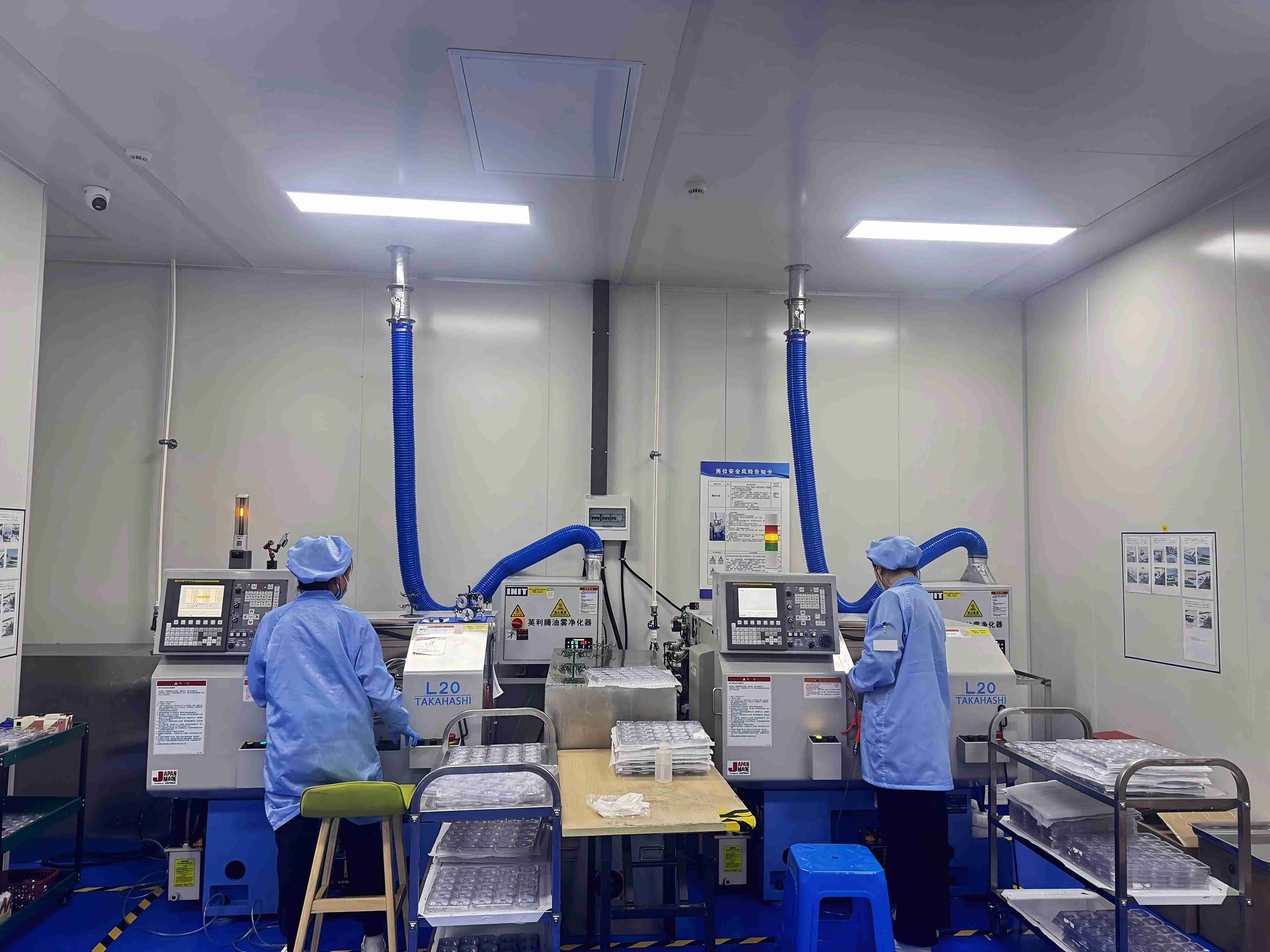
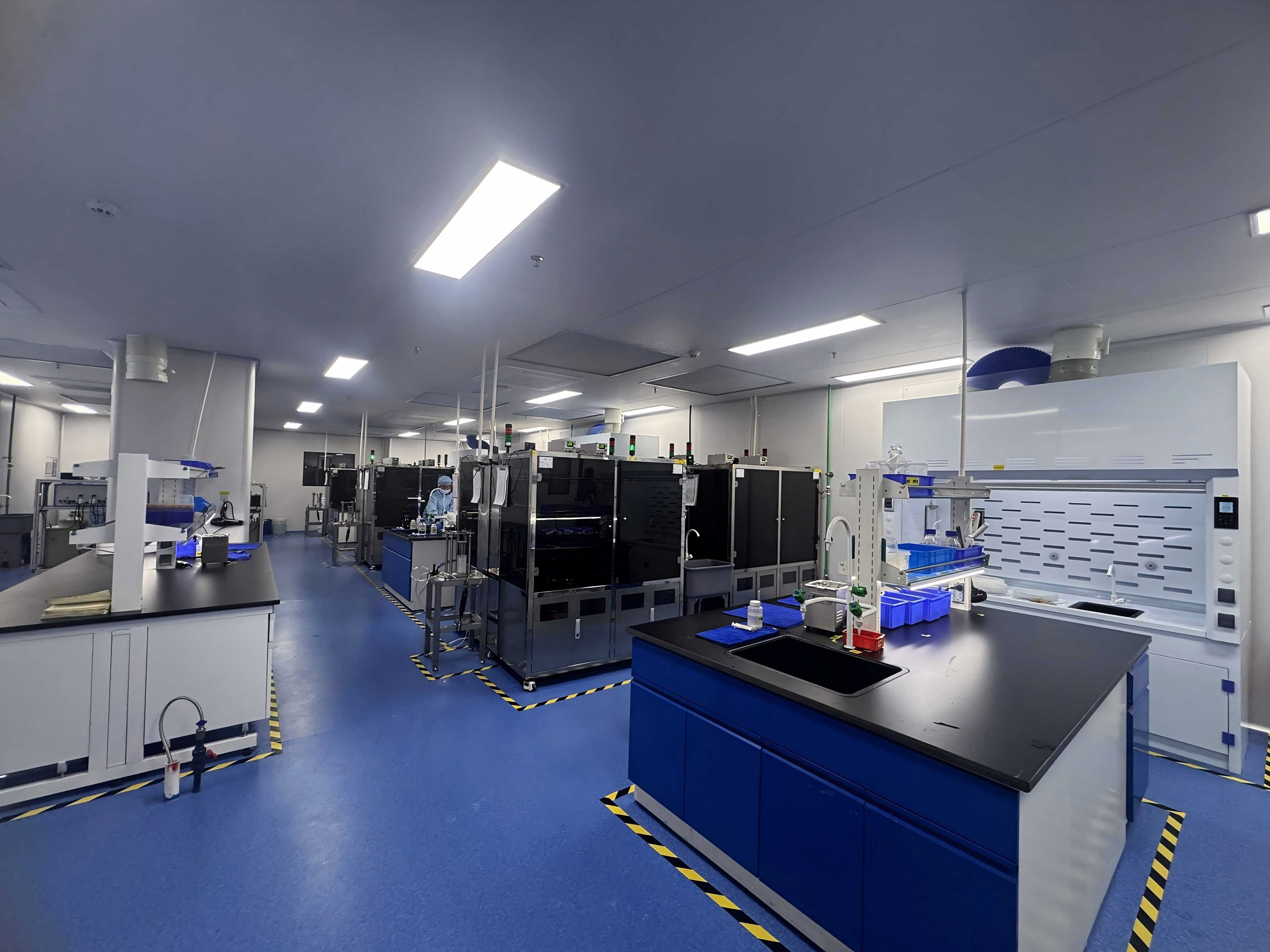
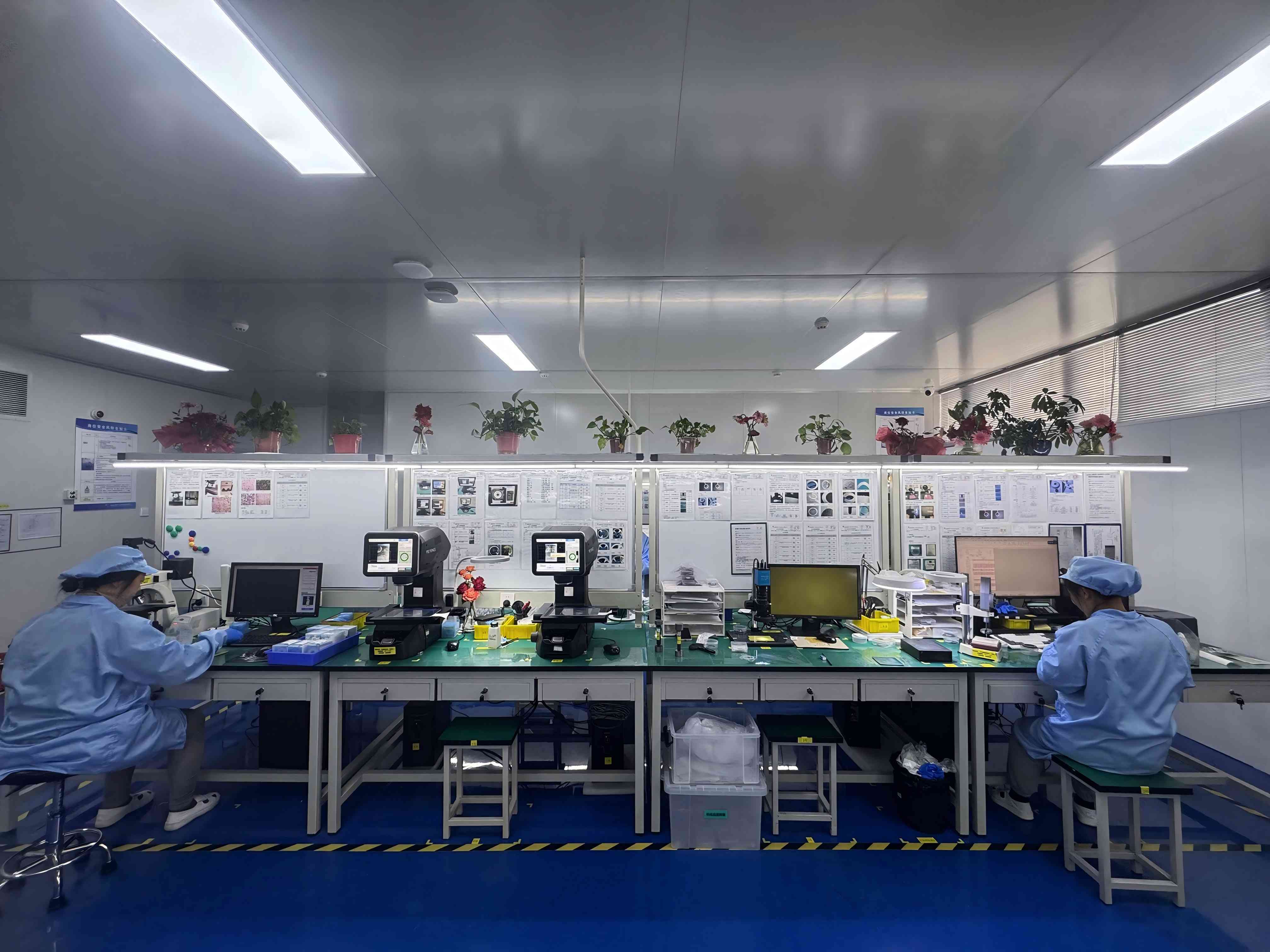
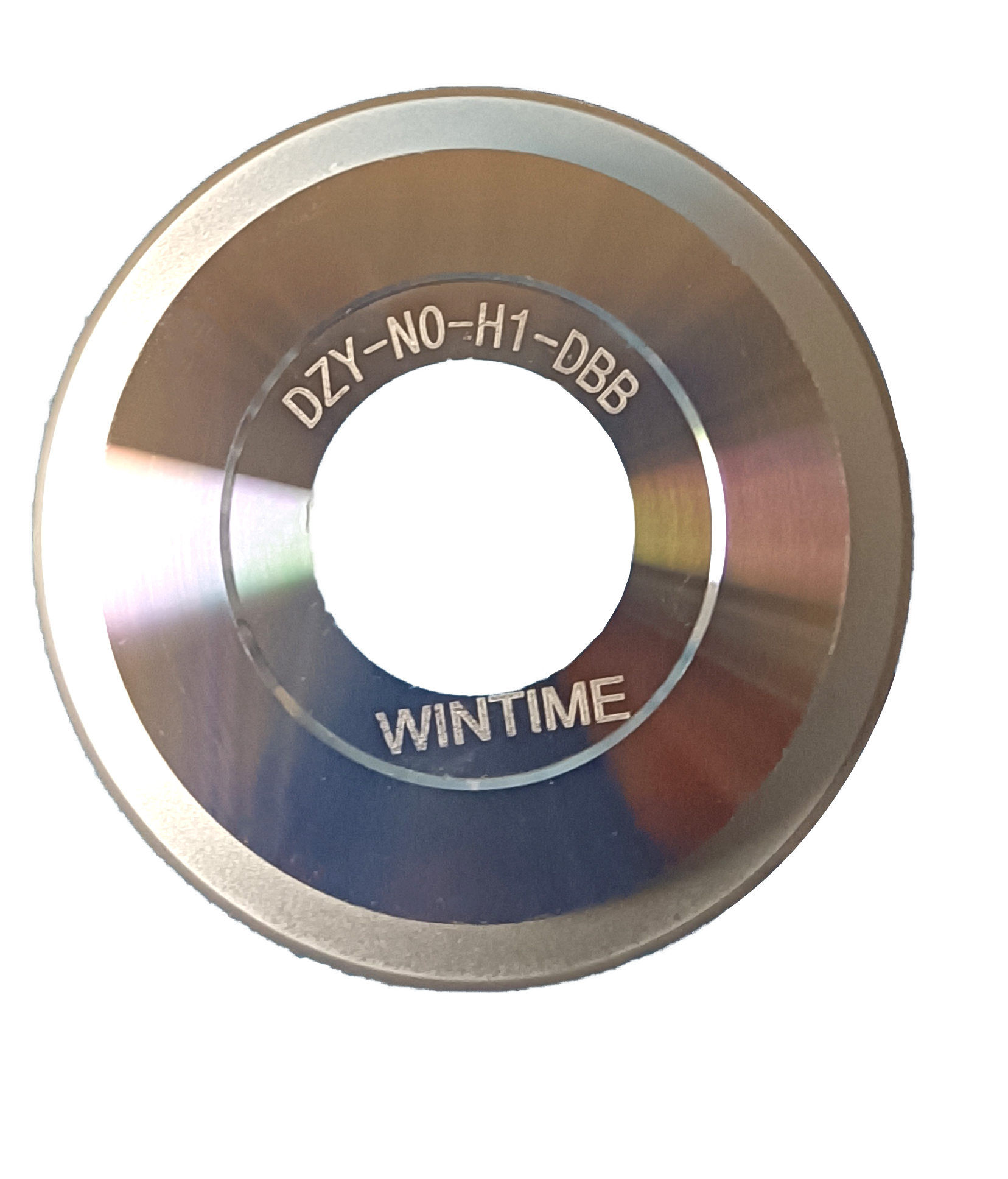
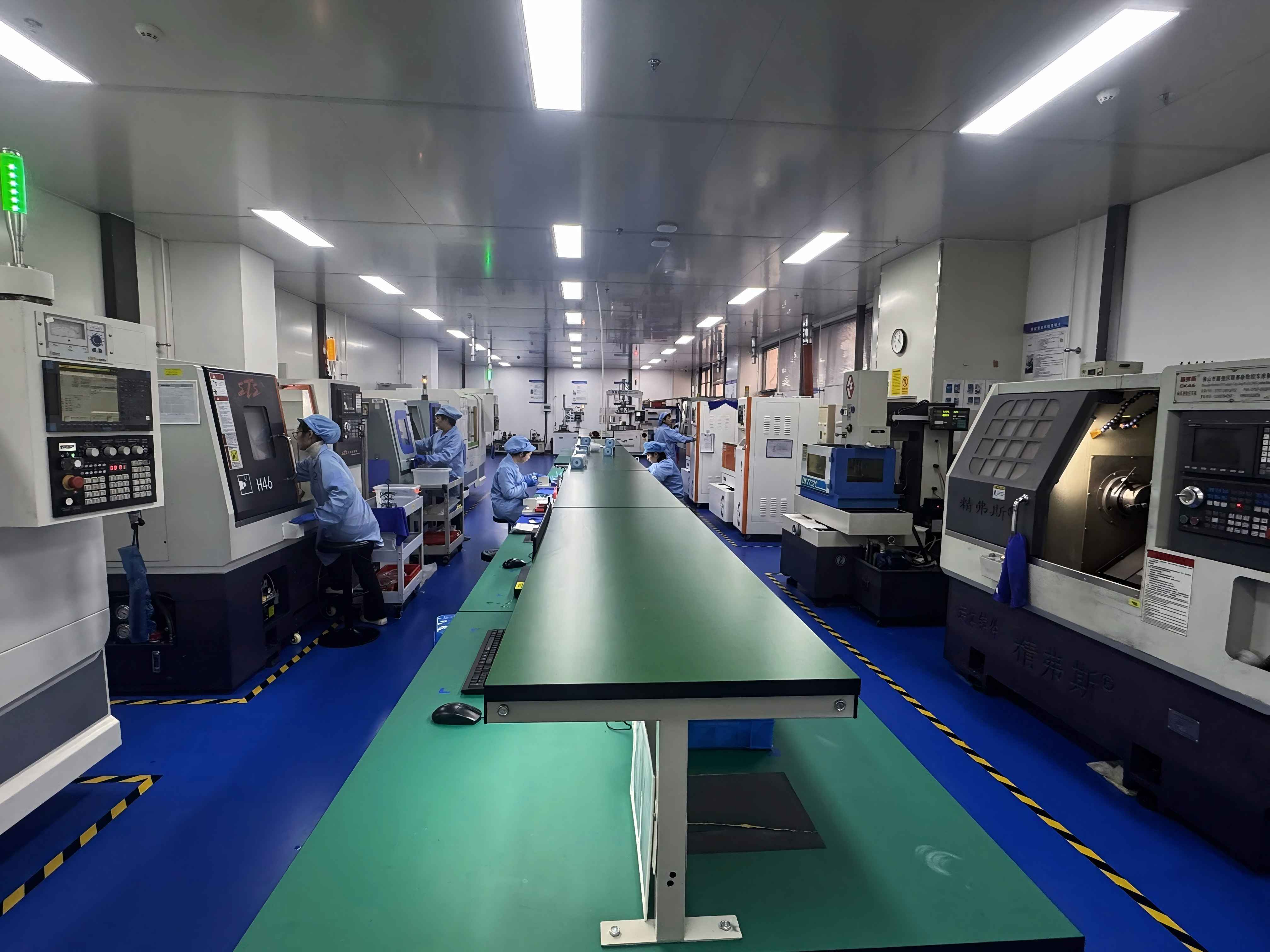
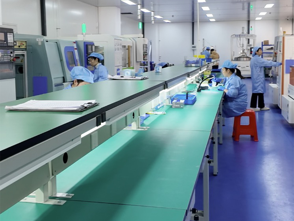
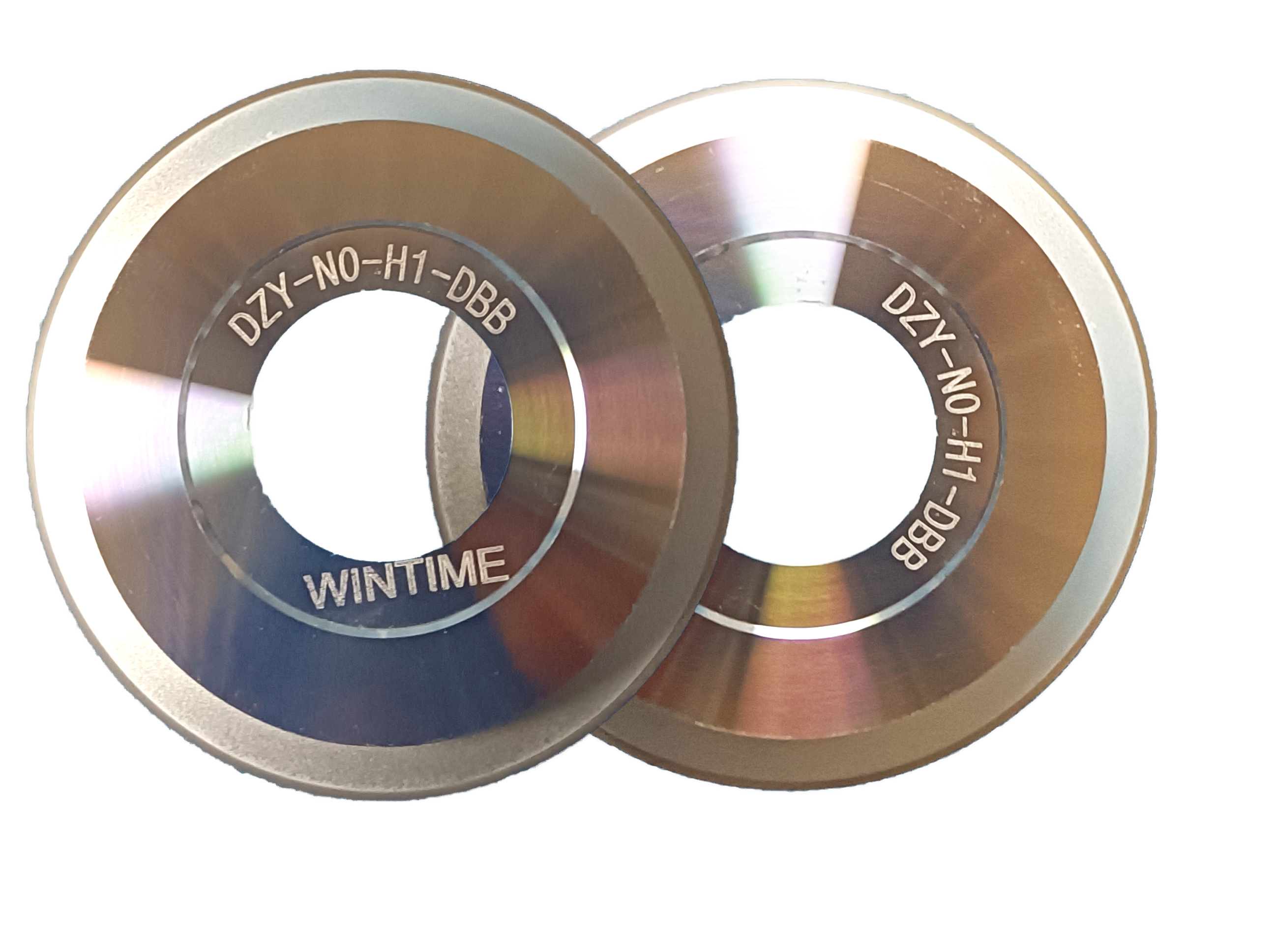
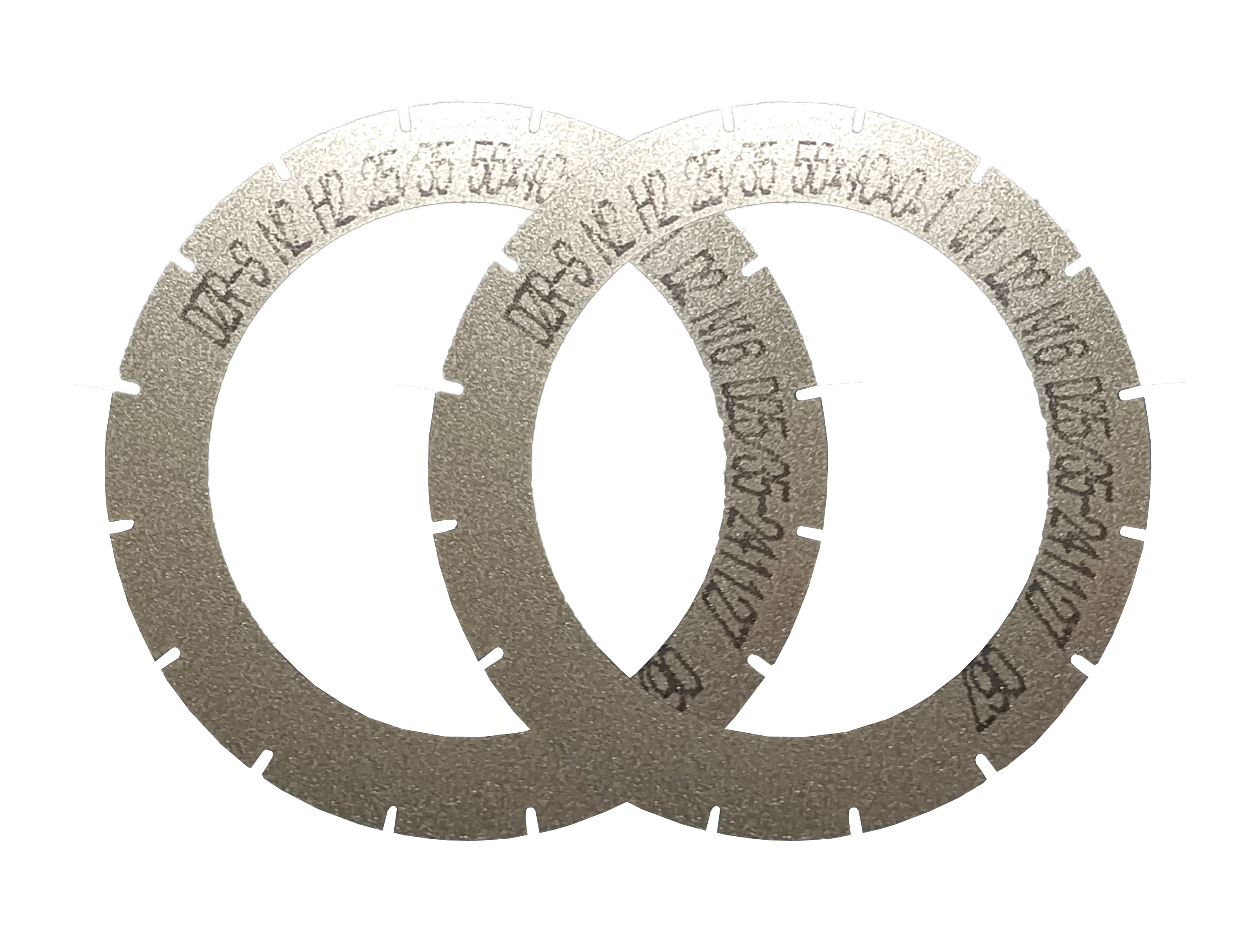
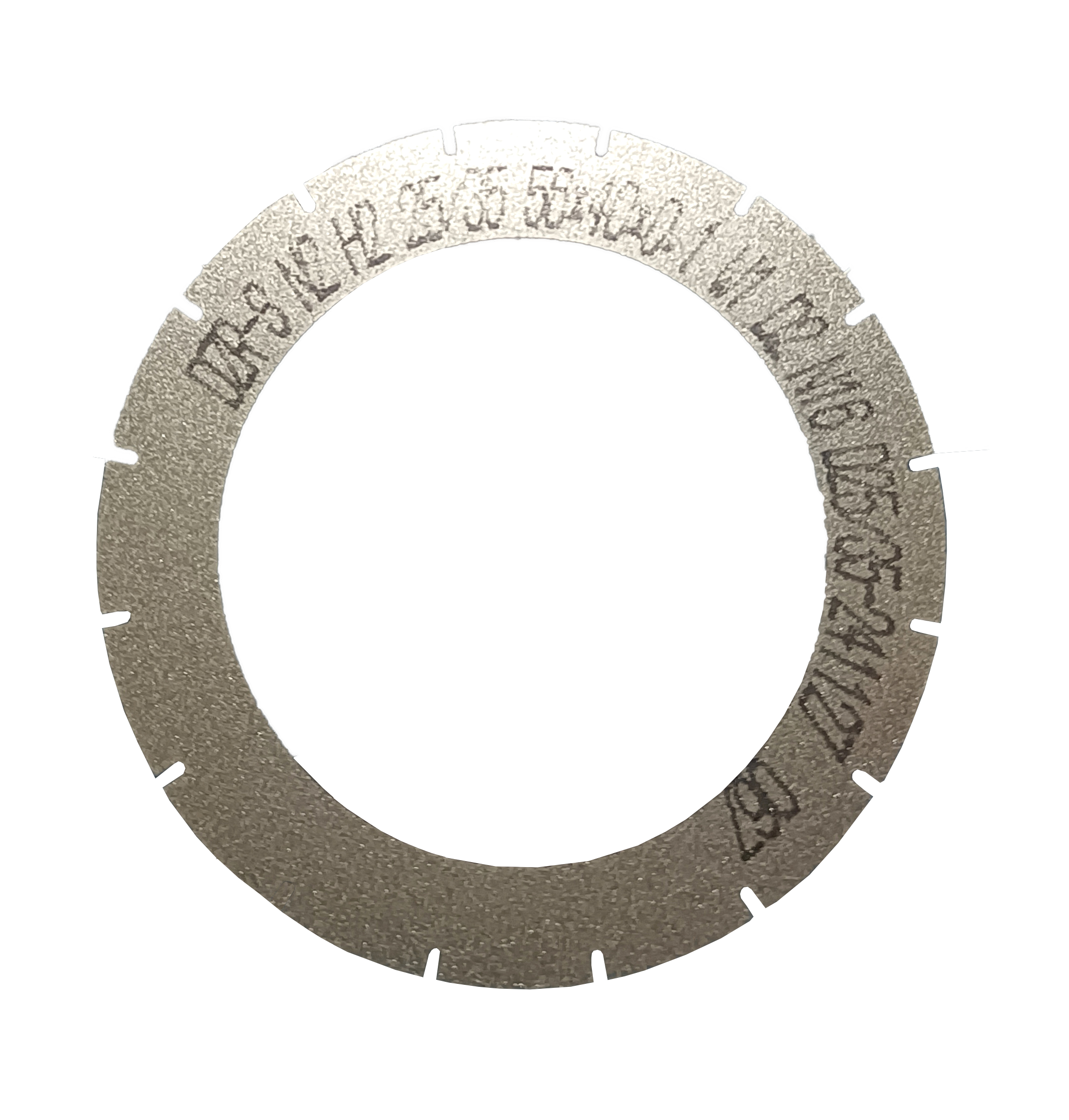
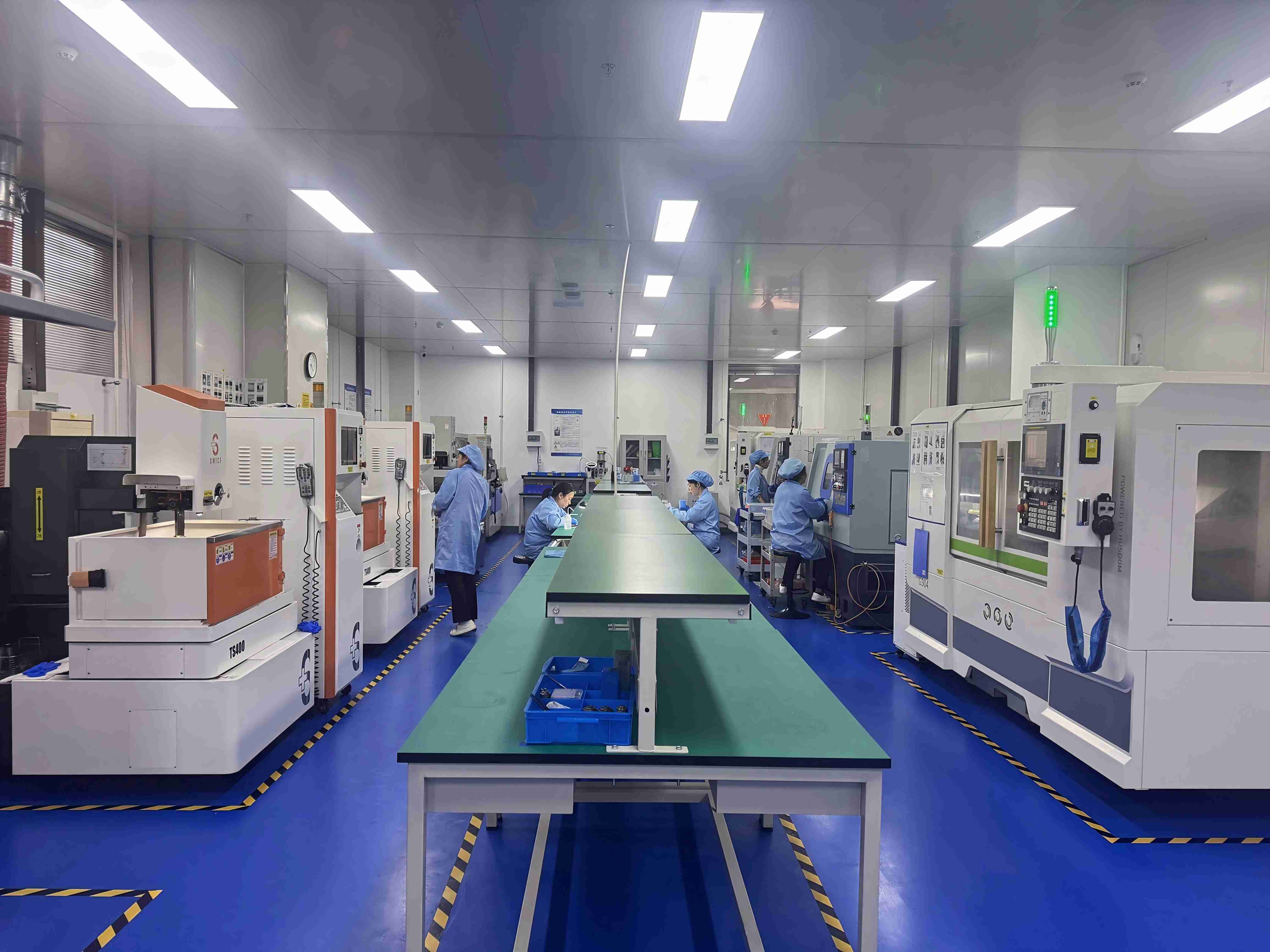
Ranked sawing blade best practices for optical communications cutting: class 100/1000 cleanroom control, static control, straight-cut accuracy and blade configuration levers.
2026-10-03 02:32:06
Application guide to sawing blade best practices in optical communications: Class 100/1000 cleanroom discipline, ESD control and straight-cut accuracy for optical modules, fiber and ceramic substrates.
2026-10-03 02:31:33
A three-gate framework for evaluating a sawing blade supplier: cleanroom output verification, written acceptance criteria with pre-shipment and SGS inspection, and delivery assurance covering MOQ, capacity and lead time.
2026-10-02 07:25:43
Application guide to dicing blade selection for ceramic substrates, optical devices, precision alloys and wafers: bond type, thickness, diamond grain size and blade body design.
2026-10-02 02:33:37
Technical guide to sawing blade bond hardness: resin vs metal bonds, HRC 65-70 specs, precision feeding steps, and why ultra-thin slicing needs blades at or below 9 um.
2026-10-02 02:26:45
Compare Sawing Blade options for optical device cutting by kerf width, chipping tolerance and anti-static needs, plus documented SB-001 specification data.
2026-10-01 07:31:20
Sawing blade sets ranked for 2026 semiconductor packaging lines: low chipping, dimensional accuracy, mass-production stability and ≤9μm ultra-thin wafer dicing blades.
2026-10-01 02:25:11
Compare single-axis and multi-axis saws for narrow kerf dicing. Learn the markers that decide blade fit: precision feeding mode, kerf constraint and radial runout limits.
2026-09-30 07:41:44
Decision-stage FAQ on long-term sawing blade supply: delivery from a 34,000 m² plant with 1 million piece annual capacity, batch consistency controls, export coverage to SEA/EA/NA/EU, and after-sales support.
2026-09-30 02:34:16
How to vet a sawing blade OEM supplier: six contract success questions, spec control, MOQ and lead time terms, quality evidence, and maintenance tips for long-term supply.
2026-09-29 06:17:18
Specify Sawing Blade parameters for Class 100/1000 cleanroom dicing: anti-static control, accuracy below 9 microns, wear resistance and stable mass production.
2026-09-29 02:31:44
Troubleshoot sawing blade breakage and dicing inconsistency in Class 100/1000 cleanrooms: parameter windows, 9-micron blade checks, bond selection, lead time and FAQ.
2026-09-28 07:11:30
An action plan for blade wear and kerf drift in high-volume wafer dicing: the Sawing Blade specifications, six process steps, and buyer FAQ for stable output.
2026-09-28 02:26:44
A working glossary of sawing blade terms for precision cutting: kerf, blade thickness, bond type, grit size, chipping, hubless construction, runout, and anti-static behaviour — and how each one changes a real specification. By WINTIME Semiconductor Technology Co., Ltd.
2026-09-27 07:01:45
How a dicing blade works: diamond grit, bond behaviour, kerf and chipping control, cleanroom conditions, and how WINTIME's Ultra-thin Wafer D Blade reaches below 9 µm thickness for semiconductor, optical, and ceramic cutting.
2026-09-27 02:28:52
Compare sawing blade requirements for optical device cutting vs. ceramic substrate cutting: cleanroom conditions, bond type, kerf, chipping, and cutting mode.
2026-09-27 02:25:08
Hubless vs. hub-type sawing blades compared for semiconductor and ceramic slicing: sub-9 μm blade stability, spindle and cleanroom needs, selection rules.
2026-09-26 07:12:18
A sawing blade cuts with a diamond bond, ultra-thin kerf and a high-speed spindle. See how it differs from a standard cutting wheel and how to specify one.
2026-09-26 02:28:52
Audit checklist for sawing blade factories: verify manufacturing area, annual capacity, engineering headcount, patents, QC records, and lead times before signing.
2026-09-25 07:16:10
How ultra-thin wafer slicing works in a cleanroom: spindle speed, dry vs wet cutting, precision feeding, Class 100/1000 conditions, and sawing blades below 9 μm.
2026-09-25 05:39:10