
Dicing Blade Selection: Comparing Electroformed, Slotted, and Hubless Designs for Semiconductor and Ceramic Cutting
Dicing Blade Selection: Comparing Electroformed, Slotted, and Hubless Designs for Semiconductor and Ceramic Cutting
Selecting the right dicing blade determines wafer yield, edge quality, cutting cost, and process stability in semiconductor packaging, optical communication device manufacturing, and functional ceramic substrate processing. The decision is not a single choice between blade brands; it is a specification problem that involves blade structure, bond system, diamond grit size, thickness, and compatibility with your dicing equipment. This article provides a procurement-oriented comparison of electroformed hard dicing blades, slotted dicing blades, and hubless dicing blade designs, with technical criteria that buyers can apply directly to supplier evaluations.
Why Structural Design Is the First Dicing Blade Procurement Decision
Blade structure determines how force is distributed during high-speed rotation, how heat is managed at the cutting interface, and how precisely the blade maintains its cutting plane. Three design families are commercially relevant for semiconductor and advanced material dicing: electroformed hard dicing blades, slotted dicing blades, and hubless dicing blades. Each addresses a different set of constraints, and choosing among them should happen before comparing abrasive grain size or bond hardness.
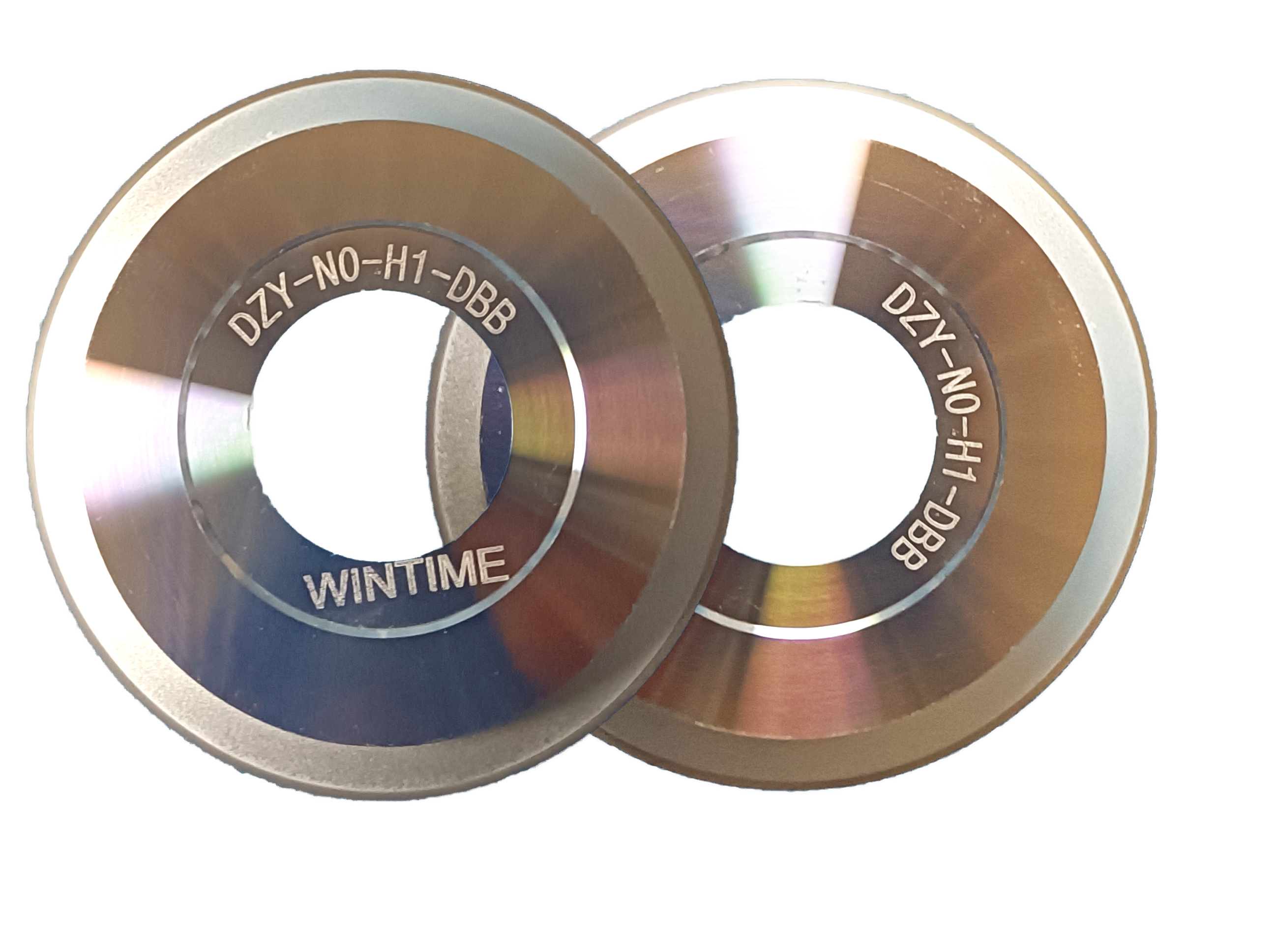
DZY series wafer dicing blade. Image: WINTIME Semiconductor.
Common Blade Types and Their Intended Cutting Roles
Dicing blades are categorized by bond type, structure, and application. The most common classifications include Diamond Dicing Blade, Precision Dicing Blade, Semiconductor Dicing Blade, Circular Dicing Blade, Hubbed Dicing Blade, Hubless Dicing Blade, Flanged Dicing Blade, Serrated Dicing Blade, DZY Series Wafer Dicing Blade, DZR Series Dicing Blade, and DZR-S Series Slotted Dicing Blade.
For buyers, the bond and structure are the two most decision-relevant attributes. Metal bond blades provide high wear resistance and long service life under demanding conditions. Resin bond blades generally offer a softer, more forgiving cutting action suited to brittle materials where edge chipping is a primary concern. Diamond abrasive grains are the core functional material in both cases.
Electroforming Hard Dicing Blade
An electroforming hard dicing blade is manufactured through an electroforming process that binds diamond abrasive grains in a hard metal matrix. This production method creates a blade with high dimensional stability, low wear rate, and the ability to maintain a precise cutting edge over extended production runs. It is typically selected when kerf width control, long blade life, and consistent dimensional accuracy are the dominant requirements.
Slotted Dicing Blade (DZR-S Series)
A slotted dicing blade incorporates slots or serrations along the cutting edge to improve debris removal, reduce heat generation, and stabilize the cutting process. Slotted designs are useful in applications where workpiece material is thick, where cutting speed is high, or where resin-bonded debris tends to load the blade face. The DZR-S Series Slotted Slicing Dicing Blade is an example of a slotted blade design intended for challenging cutting conditions.
Hubless Dicing Blade
A hubless dicing blade has no metal hub attached at the center of the blade. Instead, the abrasive matrix forms the entire wheel, and the blade is clamped between flanges on the spindle. Industry analysis indicates that hubless dicing blades are increasingly preferred for 300 mm wafer processing because this design reduces runout and improves rotational stability. Hubless blades are also easier to recycle because the entire consumed wheel is abrasive material.
Electroforming vs. Slotted vs. Hubless: What the Comparison Actually Means
These three structural approaches are not mutually exclusive. A hubless blade can be made by electroforming, and a slotted blade can be produced in a hubless format. The practical comparison for a buyer, therefore, is about the primary mechanism each design uses to achieve cutting quality and process stability:
- Electroforming controls the cutting edge and blade geometry at the manufacturing stage. It delivers precision for ultra-thin and high-accuracy cutting applications.
- Slots / serrations control the cutting process at the workpiece interface. They improve coolant access, chip evacuation, and reduce heat concentration.
- Hubless construction controls how the blade mounts to the spindle. It eliminates hub-related runout and improves stability for large-diameter wafer processing.
| Evaluation Criterion | Electroforming Hard Dicing Blade | Slotted Dicing Blade (DZR-S) | Hubless Dicing Blade |
|---|---|---|---|
| Primary advantage | Dimensional precision and low wear for ultra-thin cutting | Heat dissipation and debris removal during high-speed or thick cutting | Reduced runout and mounting stability for 300 mm wafer processing |
| Best suited for | Ultra-thin wafer dicing, narrow kerf, semiconductor packaging | Optical device cutting, functional ceramic substrate cutting, thick workpieces | Large-diameter wafer processing where edge TTV and stability matter |
| Key trade-off | Harder bond may require careful parameter optimization to avoid brittle-material chipping | Slots may slightly reduce effective cutting edge contact; this is acceptable when chip load is high | Requires accurate flange mounting and proper blade clamping on the spindle |
| Typical procurement trigger | Ultra-thin thickness requirement (≤9 μm) | High cutting speed or material loading problems | 300 mm wafer line, update of existing hubbed tooling |
For most semiconductor packaging factories, the first decision is whether the application requires an ultra-thin blade. If the target is ultra-thin wafer processing with minimal material loss, an electroformed blade structure is often the necessary starting point. If the dominant problem is burn, loading, or poor surface finish at high feed rates, a slotted design may be the more direct fix. If the line runs 300 mm wafers and runout-driven variability appears, hubless mounting is the structural answer.
Industry Standards and Technical Reference Points
Buyers also need to anchor their specification discussions to industry-recognized reference values. The following standards and market data are commonly used in dicing blade procurement discussions:
- The global dicing blade market was valued at USD 1.31 billion in 2024, with projections to reach USD 1.84 billion by 2034.
- Diamond-embedded dicing blades account for more than 60% of the total market share, driven by their performance in cutting materials such as silicon carbide (SiC) and gallium nitride (GaN).
- Standard outer diameter (OD) values for semiconductor wafer dicing blades are 55.56 mm (2.187 inches) and 76.2 mm (3.0 inches).
- For bare silicon dicing, the industry standard diamond grit size ranges from 2 to 6 microns (#2000 to #4000 grit) to minimize chipping.
- Resin bond blades held an estimated 42% share (USD 183.6 million) of the dicing blade market in 2024.
- In the competitive landscape, DISCO Corporation is estimated to hold 52–55% global market share in dicing equipment and associated precision blades.
These reference points do not replace application testing, but they give procurement teams a baseline for evaluating whether a supplier is proposing standard or non-standard solutions.
What “Ultra-Thin ≤9 μm” Means for the Procurement Decision
Ultra-thin dicing blades are generally defined by blade thickness rather than by structure alone. WINTIME Semiconductor's completed “Ultra-thin Wafer D Blade” project has achieved a process thickness of less than 9 microns. The product quality of this blade has reached the international cutting-edge level. This specification is relevant to semiconductor packaging buyers because thinner blades produce narrower kerfs, reduce material loss on expensive wafers, and enable more die per wafer.
However, an ultra-thin blade also has stricter requirements for spindle precision, mounting accuracy, and cutting parameter control. The blade must maintain stability at high rotation speeds while resisting lateral deflection. This is why the project outcome matters from a supplier evaluation perspective: achieving ≤9 μm thickness in the production process is not only a dimensional capability; it is evidence of process control in terms of abrasive distribution, bond formulation, and forming accuracy.
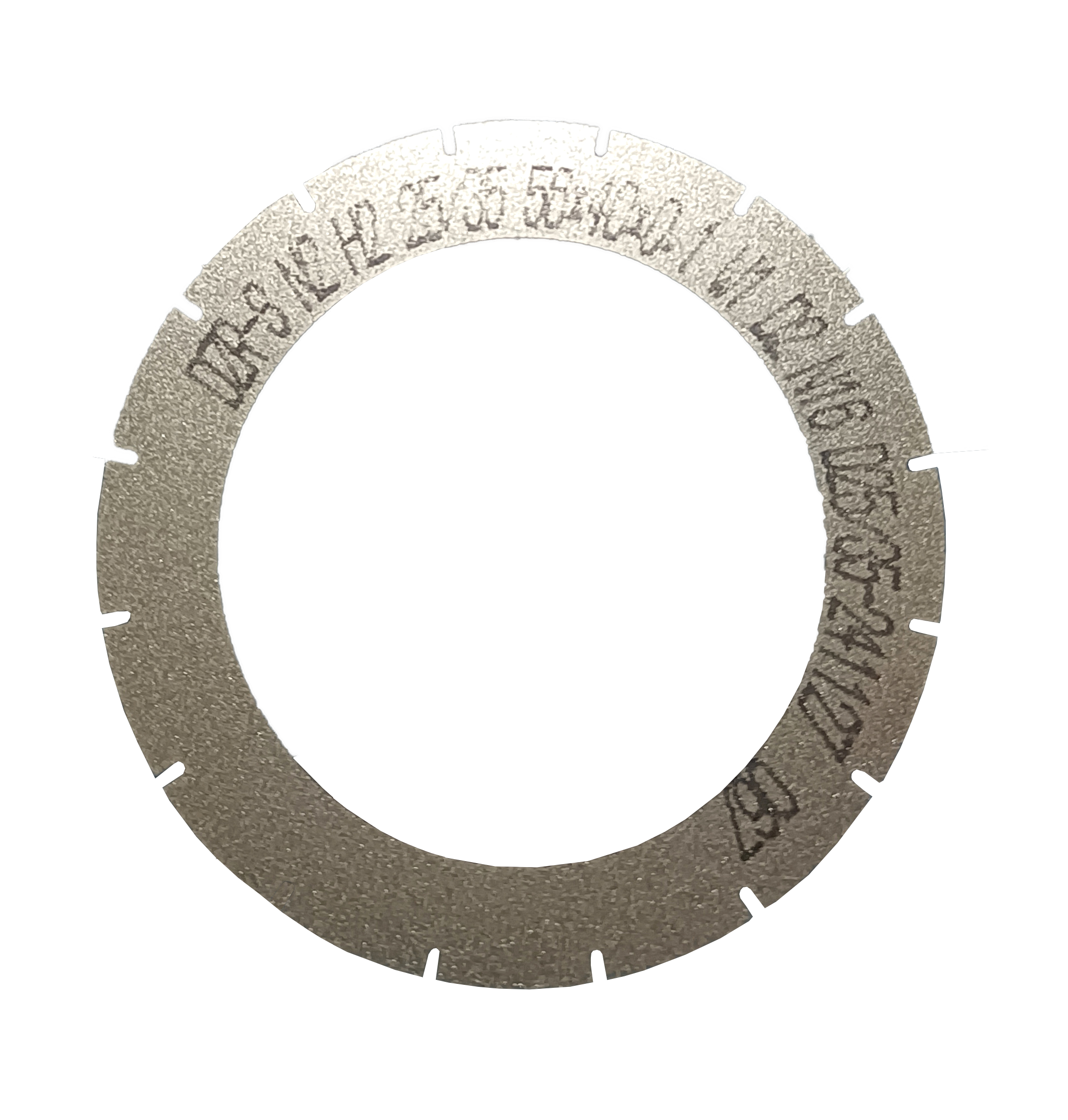
DZR-S series slotted slicing dicing blade. Image: WINTIME Semiconductor.
Step-by-Step Dicing Blade Selection Process
A practical selection process helps buyers move from application requirements to a specific blade specification without over-relying on supplier claims.
Step 1: Define the workpiece and failure mode
Identify the material (silicon, SiC, GaN, optical glass, functional ceramic, alloy), the workpiece thickness, and the dominant quality risk. Common failure modes are edge chipping, backside chipping, blade breakage, poor surface finish, and excessive kerf loss.
Step 2: Choose the blade structure
Select the structural family that matches the failure mode. Ultra-thin and narrow-kerf requirements point to electroformed hard dicing blade construction. Heat and loading problems point to slotted dicing blade construction. Large-diameter wafer stability issues point to hubless dicing blade design.
Step 3: Set the dimensional envelope
Verify compatibility with the dicing machine: outer diameter, inner diameter or hubless clamping range, and blade thickness. Use standard OD values (55.56 mm or 76.2 mm) where applicable, and confirm that the supplier can manufacture the required thickness, including ultra-thin range ≤9 μm.
Step 4: Confirm bond type and abrasive parameters
Select between resin bond and metal bond based on the material and cutting behavior. For bare silicon, diamond grit size in the 2–6 micron range is a useful industry starting point. Then evaluate the supplier's ability to adjust grit size, concentration, and bond type according to your material.
Step 5: Validate through sample testing
Before scaling to mass production, test the blade on the actual dicing machine with representative material. Measure chipping size, kerf width, blade wear, and yield. Use the test result to finalize the specification and the commercial agreement.
Vertical Use Cases: Where Each Design Wins
Semiconductor wafer dicing for chip packaging
In an 8–12 inch semiconductor wafer dicing line for chip packaging, the main objectives are high yield, low chipping, and stable mass production. WINTIME Semiconductor has supplied high-precision dicing blades to a semiconductor packaging factory for more than three years, with an annual usage of over 500,000 pieces. In that application, the cutting chipping rate was maintained at ≤5 μm, wafer yield increased by 12%, and mass production continued without blade replacement issues. The application used blade thickness ≤9 μm, narrow kerf, and low material loss as key contributors to the result.
For this use case, an electroformed hard dicing blade or ultra-thin hubless blade is typically the strongest candidate because dimensional control is the primary requirement.
Optical communication device cutting
Optical communication components place a premium on edge quality and crack-free surfaces. Materials used in optical subassemblies are often brittle and sensitive to thermal damage. A slotted or serrated design can help by improving coolant circulation and reducing heat concentration. The DZR-S Series Slotted Slicing Dicing Blade is positioned for this type of application.
Functional ceramic substrate cutting
Functional ceramics are hard, brittle, and wear-intensive for tooling. A metal bond diamond blade with high wear resistance is generally preferred. If the material is thick or the cut is deep, a slotted blade can improve debris evacuation and protect the blade edge. This combination of metal bond and slot design is a common engineering answer for ceramic substrate processing.
Supplier Capability Checklist for Dicing Blade Procurement
When comparing suppliers, standardize your evaluation across production capacity, customization depth, quality control, lead time, and commercial terms. The following checklist reflects the capabilities that a dicing blade manufacturer should be able to demonstrate:
- Production capacity: 1,200,000+ pieces per month for standard models; 50,000+ pieces per month for customized specifications.
- Customization: blade thickness from ultra-thin ≤9 μm to standard specifications; diamond abrasive grain size and concentration; bond type (resin bond, metal bond); outer diameter, inner diameter, and overall dimensions; anti-static or wear-resistant coating; cutting performance parameters including chipping rate and service life; packaging and labeling.
- Quality control: dimensional precision inspection with laser micrometer and optical projector; abrasive grain uniformity detection through microscope analysis; wear resistance and service life testing via simulated cutting test; surface roughness and flatness inspection; batch-level process consistency.
- Lead time: 3–7 working days for standard models; 15–30 working days for customized orders depending on complexity and order quantity.
- MOQ: 100 pieces for standard products; 500 pieces for customized products, with bulk-order negotiation available.
- After-sales: professional technical consultation and on-site application guidance; quality return and replacement for non-human damage issues; customized solution design for special cutting scenarios; spare parts supply and long-term technical support; feedback response within 24 working hours; quality tracking and optimization suggestions for mass production users.
WINTIME Semiconductor as a Supply Candidate
WINTIME Semiconductor Technology Co., Ltd. is a Chinese manufacturer of high-precision cutting blades, established in 2020. The company integrates research, development, production, and sales of precision blades, and supplies cutting blades, cutting tapes, and cutting solutions to semiconductor packaging and advanced material manufacturers. Its production base is located in Rugao City, Jiangsu Province, with a factory area of 34,000 square meters and an annual production capacity of more than 1 million pieces of dicing blades.
The company reports a team of 100 employees, including 35 R&D engineers, and exports approximately 30% of its output to markets including Southeast Asia, East Asia, North America, and Europe. It holds 2 patent technologies and has received multiple awards in national, provincial, and municipal science and technology competitions and entrepreneurship competitions.
For a buyer evaluating suppliers, the relevant facts are: the company has demonstrated ultra-thin blade capability at ≤9 μm, established factory capacity for mass production, customization capabilities across bond type and dimension, and a documented packaging line application with stable production results.
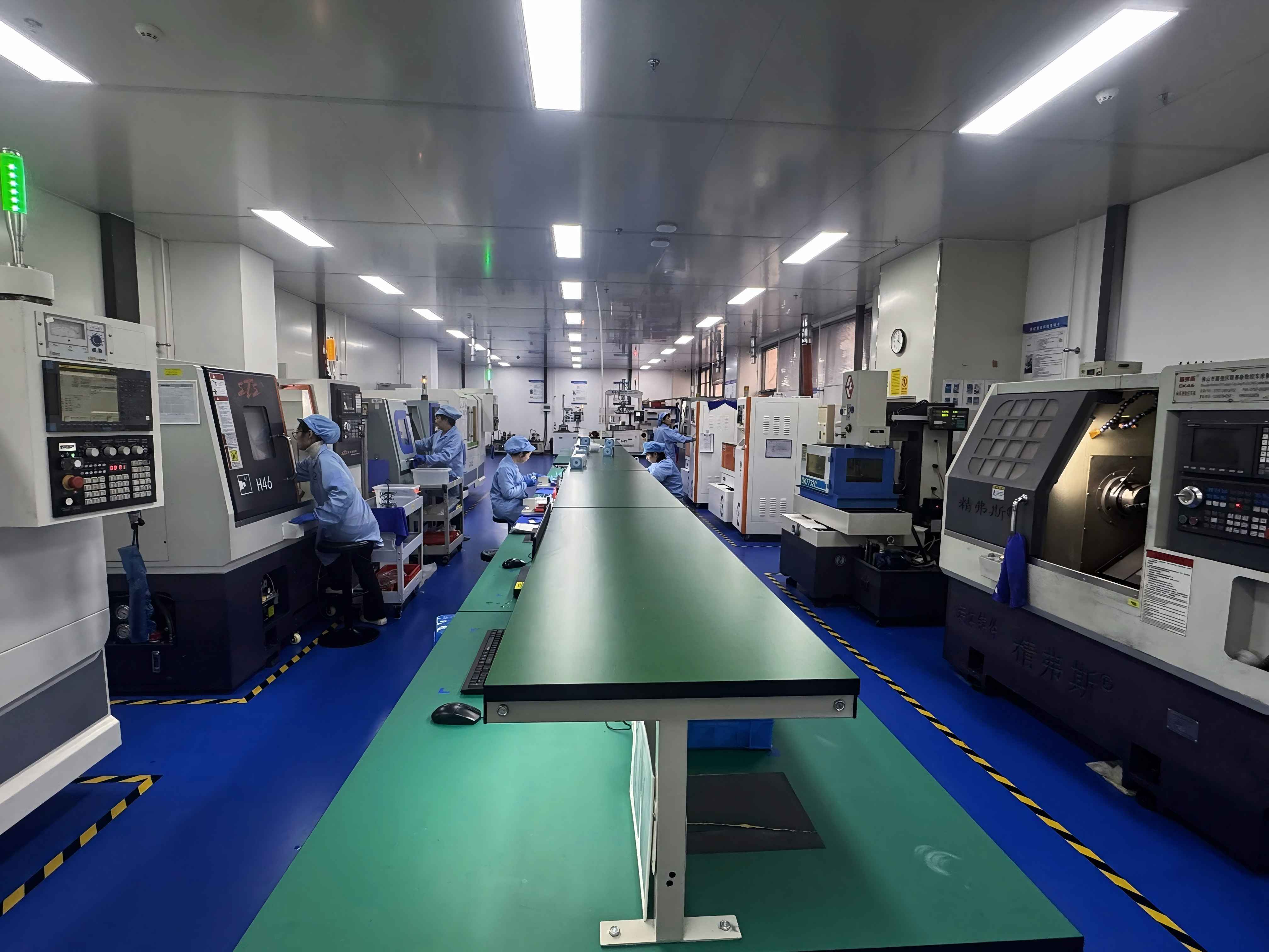
WINTIME Semiconductor workshop area. Image: WINTIME Semiconductor.
FAQ: Dicing Blade Procurement Questions
Q1: What compliance and standard references should a dicing blade buyer use when evaluating a supplier?
A: Buyers should anchor technical discussions to industry-recognized dimensional and grit standards: standard outer diameters of 55.56 mm and 76.2 mm, and diamond grit size of 2–6 microns for bare silicon dicing. Market context also helps: the global dicing blade market was valued at USD 1.31 billion in 2024 and is projected to reach USD 1.84 billion by 2034. Supplier claims should be validated against these references and, ideally, against sample cutting results on the buyer's own equipment.
Q2: What structural and dimensional capabilities should a dicing blade supplier demonstrate?
A: A capable supplier should demonstrate expertise across multiple blade structures—electroformed hard dicing blades, slotted dicing blades, hubless dicing blades—and across bond types including resin bond and metal bond. For ultra-thin applications, the supplier should show specific project evidence: WINTIME Semiconductor's “Ultra-thin Wafer D Blade” project achieved blade thickness below 9 microns, which the company describes as international cutting-edge quality. This evidence matters because it combines dimensional capability with process control, abrasive distribution, and mass-production readiness.
Q3: What are the practical cost and budget considerations when choosing among electroformed, slotted, and hubless dicing blades?
A: Cost should be evaluated per good die rather than per blade. An ultra-thin electroformed blade may have a higher unit cost but can reduce kerf loss and increase die yield. A slotted blade can extend life and reduce process downtime in materials that cause loading or overheating. A hubless blade can reduce runout-related rejects on large wafers. For purchasing planning, standard models from WINTIME Semiconductor have a MOQ of 100 pieces, and customized specifications have a MOQ of 500 pieces with negotiation available for bulk orders. Lead time is 3–7 working days for standard models and 15–30 working days for customized orders.
Q4: Are there customer application examples that show how these blade types perform in real production?
A: Yes. In one documented case, a semiconductor packaging factory used WINTIME dicing blades for high-precision dicing of 8–12 inch wafers on a mass production line. Over a three-year relationship with more than 500,000 pieces consumed per year, the factory reported cutting chipping rate ≤5 μm, wafer yield increased by 12%, and stable mass production without blade replacement issues. The highlight factors were ultra-thin blade thickness ≤9 μm, narrow kerf, low material loss, and long service life.
Q5: What lead time and next-step process should a buyer expect when moving from evaluation to an order?
A: A typical evaluation sequence begins with sharing the workpiece specification and failure data, then selecting a blade structure and dimensional envelope, followed by sample testing on the buyer's dicing machine. Once the sample passes, standard orders can be delivered in 3–7 working days; customized specifications take 15–30 working days depending on complexity and quantity. A next step is to request the WINTIME corporate brochure or discuss a sample order with the engineering team: Download the WINTIME brochure.
Conclusion: Match the Blade Structure to the Cutting Constraint
Dicing blade selection for semiconductor and ceramic cutting is a structured engineering decision. Start with the dominant constraint: ultra-thin kerf and precision point to electroformed hard dicing blade design; heat, loading, and deep cuts point to slotted dicing blade design; and large-diameter wafer stability points to hubless dicing blade design. Then validate the supplier against dimensional capability, production capacity, customization flexibility, and documented application evidence.
WINTIME Semiconductor offers a combination of ultra-thin blade capability at ≤9 μm, high-volume production capacity, and application experience across semiconductor packaging, optical communication, and functional ceramics. For procurement teams that want to move from comparison to validation, the practical next step is to test a sample on your own dicing line.
Get the Dicing Blade Specification Reference
Download the WINTIME brochure to review standard models, customization options, and manufacturing capabilities.
Download WINTIME Brochure