
Fixing Chipping and Micro-Cracks in Semiconductor Package Cutting: Sawing Blade Solutions
Chipping and micro-cracks in semiconductor package cutting are fixed at the blade–material interface, not at the inspection station. On most package sawing lines the two defects share one origin: the sawing blade removes a brittle, multi-material stack faster than that stack can tolerate, and part of the damage stays below the surface where it is invisible until reliability testing or downstream assembly opens it up.
This article is written for teams that have already decided to act — process engineers, package sawing line owners and procurement staff who now need a blade specification they can execute and keep executing. It defines what the two defects actually are, explains why package cutting is harder on a blade than plain wafer dicing, identifies the blade characteristics that control chipping, sets out the changeover step by step, and shows how to hold the result steady across production batches and repeat orders.
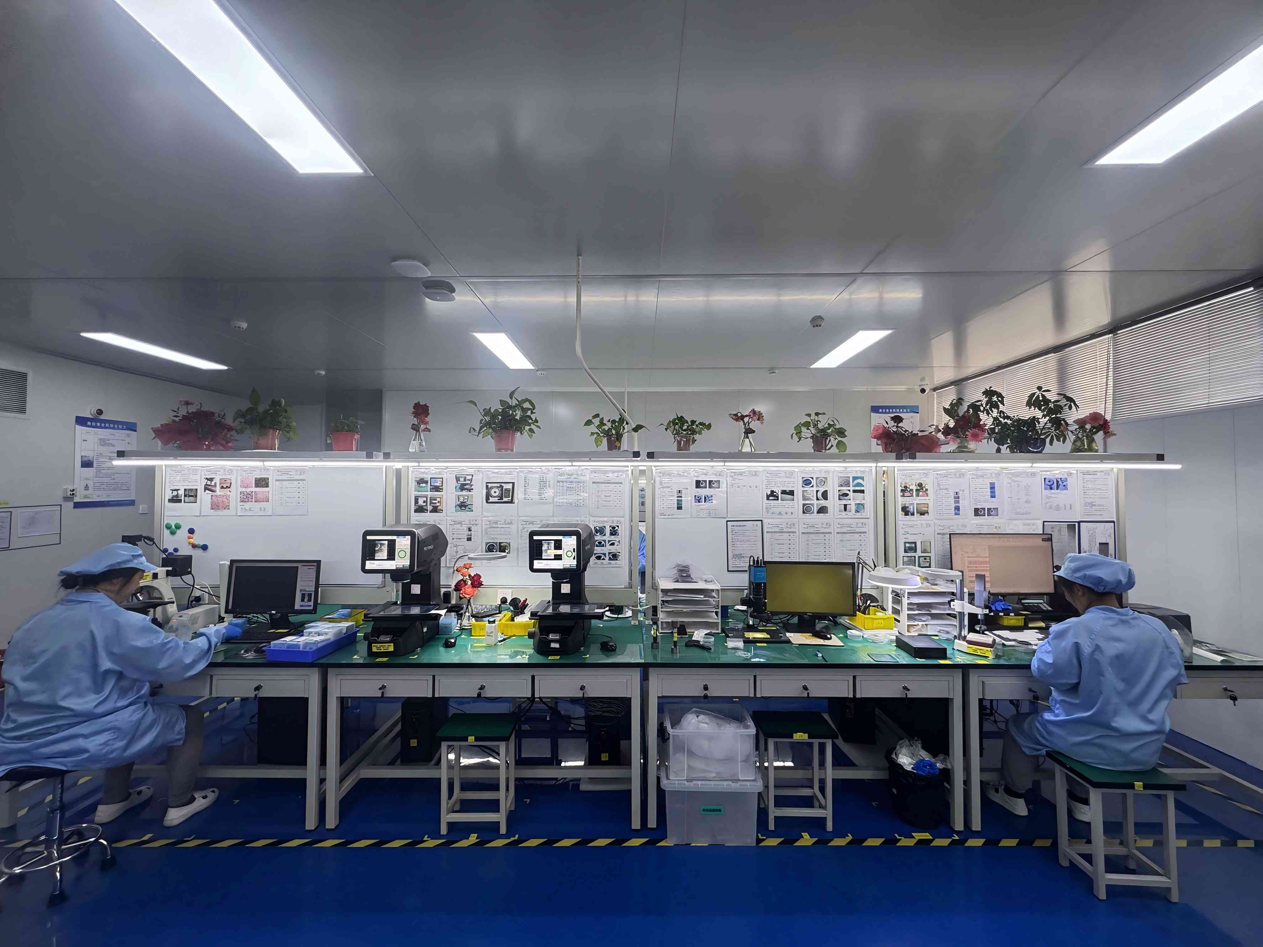
Sawing blade production at WINTIME Semiconductor Technology Co., Ltd., Rugao City, Jiangsu Province.
What Chipping and Micro-Cracks Actually Are
Chipping is edge material loss at the cut boundary. Fragments of molding compound, substrate or die edge break away instead of being sheared cleanly, leaving a ragged kerf wall, a missing corner or a scatter of loose particles on the die surface. Chipping is visible immediately and is normally measured as the largest chip on a die perimeter.
A micro-crack is a subsurface crack that starts at the kerf wall and propagates into the package body, frequently running parallel to the cut. The cut face can look acceptable under ordinary inspection while the crack is already present, which is why micro-cracks usually surface later — after thermal cycling, after molding, or after the part has been assembled into a module.
The two defects are related but not identical, and confusing them leads to the wrong blade change:
- Chipping is a mechanical overload event at the cut edge. It responds to entry and exit conditions, blade runout, grit size and feed rate.
- Micro-cracks are accumulated subsurface damage. They respond to cutting force per unit of diamond contact, which is governed by bond hardness, diamond exposure and how many passes the blade takes through the material.
- Both share one amplifier: a blade that has lost its sharpness. A worn blade stops cutting and starts crushing, and crushing produces chips and cracks at the same time.
Why Semiconductor Package Cutting Is Harder on a Sawing Blade Than Wafer Dicing
The dicing blade market was valued at USD 1.19 billion in 2024, driven by semiconductor miniaturization and the shift to 300 mm wafers, according to Market Research Intel. Within that market, resin bond blades held a 42% share in 2024 while metal bond blades — the type used for harder materials such as SiC — accounted for 33%, as reported by market.us. Those proportions describe a blade supply base built largely around silicon, yet a growing share of the cutting work now happens on packages rather than on bare wafers.
The difference matters because a package cut is a multi-material cut. A single kerf can cross molding compound, a substrate or leadframe, a die edge and sometimes a metal or dielectric layer. Each of those materials removes material by a different mechanism: molding compound with its silica filler is abrasive and wears the bond, while metal layers smear and load the diamond. A blade tuned for homogeneous silicon enters this mix under-matched, and the first symptoms are edge chipping at the compound interface and micro-cracks where the blade passes from filler-rich compound into metal.
Two structural trends reinforce the pressure. First, hubless dicing blades are increasingly dominant for 300 mm wafer processing because of their stability and reduced runout on substrates thinner than 50 µm, a trend documented in current semiconductor equipment market data. Reduced runout is directly relevant to chipping, since runout is what converts a steady feed into a series of impacts at the kerf wall. Second, the application mix is broadening: optical communication and RF/optoelectronics accounted for 16% of dicing blade market share in 2024 — USD 69.9 million — driven by 5G infrastructure expansion, per Intel Market Research. Devices in that segment are frequently small, brittle and expensive per unit, so a chipping problem there is a yield problem, not a rework problem.
The reference framework for describing diamond cutting tools is ISO 22180:2019, which distinguishes CVD diamond-coated types from monocrystalline and polycrystalline types. That classification is the baseline vocabulary on a blade datasheet; it does not by itself predict chipping performance. Nor is the supply side narrow — the leading players in high-precision semiconductor dicing blades include DISCO Corporation, Tokyo Seimitsu (Accretech), Advanced Dicing Technologies (ADT) and Asahi Diamond, per Credence Research. Buyers therefore have real alternatives, which is precisely why the specification has to be written in terms of blade behavior rather than brand labels.
The Blade Prescription: Three Properties That Control Chipping and Micro-Cracks
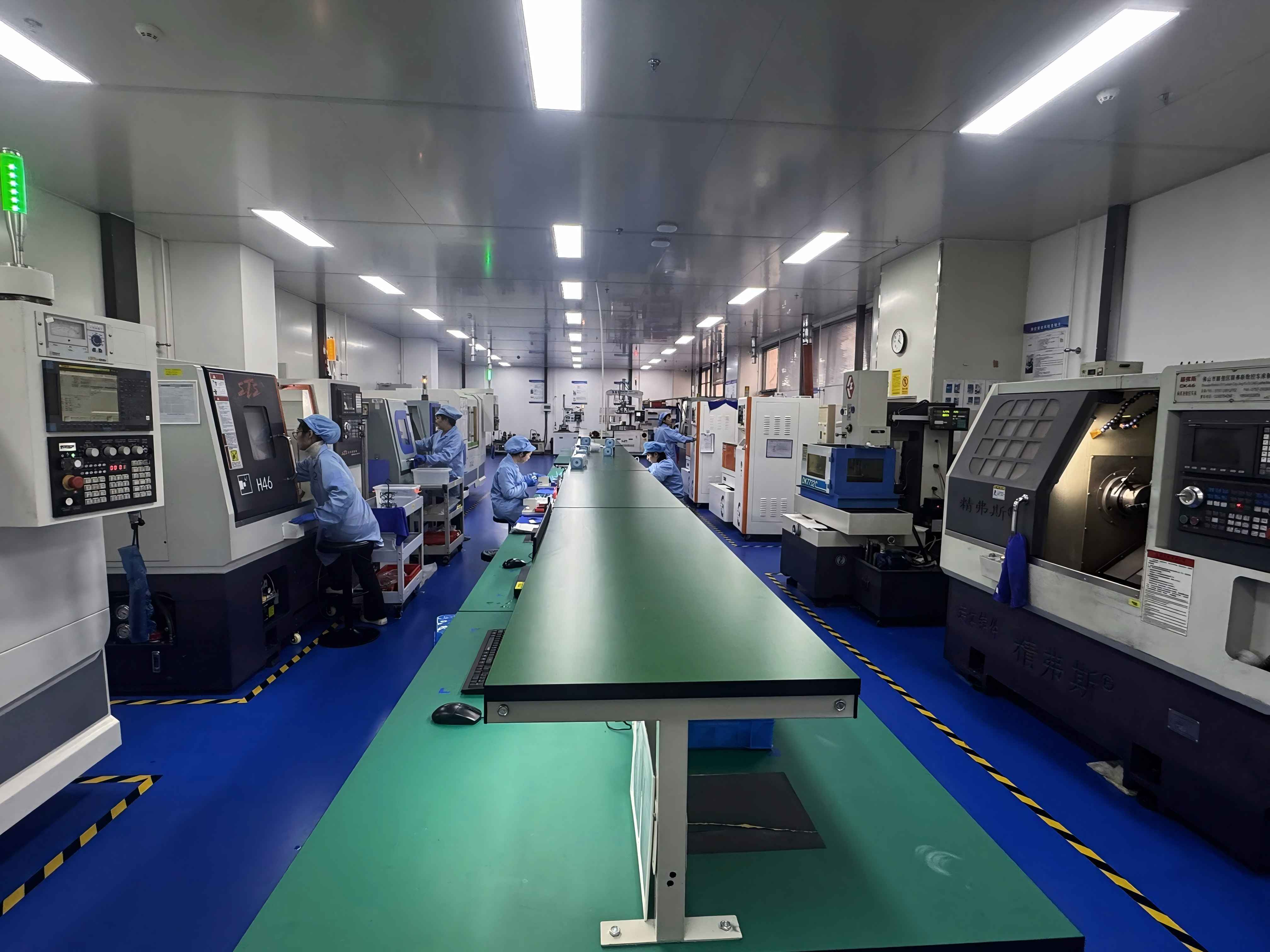
Process-controlled sawing blade production: parameter discipline is what makes a chipping fix repeatable.
1. Low-chipping design: control where the diamond meets the edge
Low chipping is a design outcome, not an inspection result. It comes from three design decisions taken together: a diamond grit size matched to the smallest feature on the package rather than to cutting speed; a bond that holds each diamond until it is genuinely dull and then releases it cleanly, so the blade never runs with a mix of polished and fresh grit; and a blade body with enough stiffness that the kerf wall sees a cutting edge instead of a wobble.
The body decision is where the hubless format earns its place. On thin substrates, a hubless sawing blade reduces runout at the cutting edge, which lowers the impact load at entry and exit — the two points where package chipping most often begins. WINTIME Semiconductor Technology Co., Ltd. supplies hubless sawing blades alongside its DZY Series wafer sawing blades, DZR Series sawing blades, DZR-S Series slotted sawing blades and electroforming hard sawing blades, so the body and bond format can be matched to the package stack rather than forced onto it.
2. High wear resistance: hold the cut through the whole blade life
Wear resistance is usually discussed as a cost issue — how many pieces per blade. In a package cutting line it is a defect issue first. A blade that wears too quickly changes its own cutting geometry mid-run: diamond exposure drops, the bond starts contacting the work, and the blade transitions from cutting to burnishing. The result is a chip-size distribution that drifts upward across a lot, which is far harder to detect than a sudden failure and far more damaging to yield.
A wear-resistant bond keeps diamond exposure inside a stable band for the whole working life of the blade, so the chipping signature at piece 1,000 resembles the signature at piece 100. For hard and brittle work — functional ceramics, hard alloys, electroformed hard blades used on demanding stacks — this stability is the difference between a qualified process and a process that needs re-tuning every shift.
3. Precision feeding compatibility: match the blade to the saw, not the reverse
A blade that can only perform inside a narrow feed window is a production risk. Precision feeding compatibility means the blade is designed to hold its chipping performance across the feed range the package saw actually uses — including entry and exit ramps, where feed is intentionally reduced, and steady-state cutting, where it is not.
This is where many chipping projects stall. The blade is replaced, chipping improves for a few days, then returns because the feed recipe still pushes the blade past the point where the bond can keep diamond exposed. The practical rule is to change the blade and the feed window as one package: a low-chipping blade paired with a step-cut or multi-pass strategy, and a wear-resistant bond paired with a feed rate the saw can repeat exactly.
Step-by-Step: Executing the Fix on a Package Sawing Line
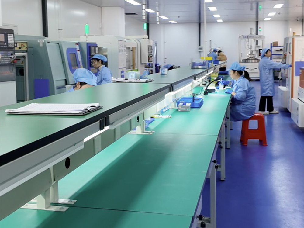
Batch-level parameter tracking: the record that lets a chipping fix survive a repeat order.
Where the Prescription Applies: Package and Device Scenarios
Optical communication and RF/optoelectronic packages
This segment accounted for 16% of dicing blade market share in 2024, at USD 69.9 million, according to Intel Market Research. Devices here are typically small, brittle and high-value per unit, so a single micro-crack that propagates after thermal cycling removes the whole part. Low-chipping geometry plus a feed window with reduced entry speed is the starting prescription; a hubless body helps where the substrate is thin enough that runout dominates.
Functional ceramic substrates
Ceramics fail differently from molding compound: chipping appears as conchoidal breakout rather than filler-driven edge loss, and the material is unforgiving of any blade wobble. Electroforming hard sawing blades and a step-cut strategy address the crushing mechanism that produces micro-cracks in brittle ceramic. The trade-off is speed — ceramic cuts that prioritize chipping performance will run slower than a pure throughput recipe, and that trade-off should be decided before qualification, not after.
Precision alloy and metal-containing package stacks
Metal layers load the diamond and smear rather than cut cleanly. Alloy material sawing blades need a bond that resists loading and a grit that stays exposed when the metal tends to plate onto the blade. Where a kerf crosses both compound and metal, expect the chipping signature to change at the interface — that step is the diagnostic point for whether the bond is holding exposure correctly.
Semiconductor wafer and thin-die cutting
For thin wafers, chipping and micro-cracks are strongly driven by runout and by blade stiffness. WINTIME's completed "Ultra-thin Wafer D Blade" project achieved a thickness below 9 microns in the process, and the product quality reached the international cutting-edge level; it is one of the few domestic companies able to mass-produce at that thickness. Thin-blade capability matters here because kerf loss and blade stiffness are in direct conflict, and resolving that conflict is a blade design problem rather than a saw setting problem.
Chipping and Micro-Crack Troubleshooting Matrix
Use the defect signature to decide which blade property to change first, then verify with the measurement method in the last column. The matrix describes cause–response logic, not a fixed recipe; the correct feed window still has to be established on the actual package stack.
| Defect signature | Most likely blade-side contributor | Blade or process response | How to verify |
|---|---|---|---|
| Chipping concentrated on one side of the kerf | Runout at the cutting edge, body seating or hub condition | Move to a hubless body format; check blade mounting and spindle condition | Chip-size map across the full die perimeter, compared before and after |
| Random chipping spread across the cut | Bond grade releasing diamond unevenly; grit too coarse for the feature size | Change bond grade first, then grit; re-check wear resistance over blade life | Chip-size distribution at start, middle and end of blade life |
| Micro-cracks parallel to the cut, found after reliability testing | Excess cutting force per pass; blade burnishing instead of cutting | Step cutting with reduced depth per pass; confirm feed stays inside the blade's window | Cross-section of a sample lot, not optical inspection alone |
| Breakout at package corners and at compound–metal interfaces | Entry and exit impact load | Reduce feed at entry and exit; review tape adhesion and chuck support | Targeted inspection of corner locations on the die map |
| Chip size drifting upward late in blade life | Wear-driven loss of diamond exposure | Select a more wear-resistant bond; set a blade-change interval based on pieces cut | Trend chip size against cumulative pieces cut per blade |
Keeping the Fix Stable: Batch Consistency and Long-Term Supply
A chipping fix that works on the qualification lot and fails three months later is not a fix. Two things protect it: a blade whose design does not vary between batches, and a supplier whose production system is built to reproduce parameters rather than to reproduce output volume.
On the production side, WINTIME Semiconductor Technology Co., Ltd. operates an ISO 9001 quality management system and follows standard operating procedures, assigns dedicated quality inspectors to track each production batch, standardizes process parameters on automatic production equipment to remove manual operation error, and keeps a batch quality file that is traceable at any time. Comparative testing of adjacent batches is used to confirm that performance has not shifted before a new lot is released into a customer's volume line.
On the supply side, capacity determines whether the fix can be scaled rather than only proven. WINTIME's factory in Rugao City, Jiangsu Province covers 34,000 ㎡ with a research and development team of 35 engineers, and its monthly production capacity exceeds 800,000 pieces for standard specifications and 80,000 pieces for customized and special-shaped products. The Nantong WINTIME Semiconductor Special Materials Project, launched in 2023 with a total investment of nearly tens of millions of yuan, supports an annual production capacity of more than 1 million pieces of dicing blades. The company was established in 2020 and exports to Southeast Asia, East Asia, North America and Europe, with exports accounting for 30% of output — a distribution profile that reflects the wider regional shift in cutting blade trade, where China's exports to Vietnam grew by USD 18 million and to India by USD 12 million between 2024 and 2025, according to OEC data.
For buyers converting a chipping project into a repeat supply arrangement, the commercial framework is straightforward and worth writing into the trial order: MOQ of 100 pieces per order for standard models, negotiable for long-term cooperative customers or bulk purchase plans; 500 pieces per order for customized models, with flexible MOQ adjustment for small-batch trial orders below 500 pieces against a slight price adjustment based on customization complexity. Delivery terms are FOB or CIF, payment terms 30/70, and acceptance is based on pre-shipment testing with third-party inspection available through SGS.
Frequently Asked Questions
Diamond tools, including sawing blades, are categorized under ISO 22180:2019, which distinguishes between CVD diamond-coated and monocrystalline or polycrystalline types — this is the reference buyers use to describe diamond type consistently on a datasheet. On the manufacturing side, WINTIME Semiconductor Technology Co., Ltd. operates an ISO 9001 quality management system with standard operating procedures and dedicated quality inspectors per production batch. For orders, acceptance is based on pre-shipment testing, with third-party inspection by SGS available, and the inspection scope should be agreed before the first batch is produced.
No. A blade controls the blade-side contributors — diamond retention, runout, bond wear and cutting force per pass — but it cannot compensate for a feed recipe that pushes past the bond's capability or for chuck and tape conditions that let the workpiece move. In practice the blade and the feed window must be changed together. WINTIME supplies hubless sawing blades, DZY Series wafer sawing blades, DZR Series sawing blades, DZR-S Series slotted sawing blades and electroforming hard sawing blades so that body format and bond grade can be matched to the package stack, and its "Ultra-thin Wafer D Blade" project achieved a thickness below 9 microns in mass production.
For standard models the MOQ is 100 pieces per order, negotiable for long-term cooperative customers or bulk purchase plans. For customized models the MOQ is 500 pieces per order; small-batch trial orders below 500 pieces can be handled with a flexible MOQ adjustment and a slight price adjustment based on customization complexity. Delivery terms are FOB or CIF, and payment terms are 30/70.
Start with a small-batch trial order, then run the comparative test the production line already uses for qualification: measure chip size at the same die map positions and cross-section a sample to check for subsurface micro-cracks. Acceptance can combine pre-shipment testing with third-party inspection by SGS. Because WINTIME keeps batch production data and a traceable batch quality file, the parameters used on the trial batch can be compared directly against the following batches rather than being reconstructed from memory.
Capacity is sized for both standard and custom demand: monthly production capacity exceeds 800,000 pieces for standard specifications and 80,000 pieces for customized and special-shaped products, with annual dicing blade capacity above 1 million pieces. Repeatability is protected by standardized process parameters on automatic production equipment, dedicated quality inspectors tracking each batch, comparative testing of adjacent batches, and a batch quality file that allows prompt recall of an unqualified batch if a problem appears. To discuss a trial order or request a quote, contact the team at shenxiangfei@ntwintime.com or review the WINTIME product brochure.
Conclusion
Chipping and micro-cracks in semiconductor package cutting are solved by specifying a blade in three dimensions at once — low-chipping design, wear resistance that holds diamond exposure across the blade's life, and precision feeding compatibility with the saw's real feed window — and then by proving that specification holds on every batch. The blade change is the visible step; the parameter record and the batch comparison are what keep the defect from returning.
WINTIME Semiconductor Technology Co., Ltd. is a manufacturer of high-precision wafer-level cutting blades and cutting solutions, established in 2020 and based in Rugao City, Jiangsu Province, supplying sawing blades and dicing blades to customers in Southeast Asia, East Asia, North America and Europe through a 34,000 ㎡ facility with a 35-engineer R&D team.
Next Step: Test the Prescription on Your Own Package Stack
Send the defect signature — chip location map, package stack description and current feed parameters — and the team can match a blade format to the failure mode instead of to a catalogue category. Trial orders below 500 pieces are possible on customized formats with a flexible MOQ adjustment.
Email: shenxiangfei@ntwintime.com · Tel: +86 13851530812 · WhatsApp: +86 18888053207 · Website: en.wintime.net.cn
Address: No. 868, Fushou East Road, Rugao City, Jiangsu Province · Download the product brochure (PDF)

Technical and order support for sawing blade trials and repeat supply.
Have Questions or Need More Details?
Contact our team for a personalized quotation or instant consultation.
Request a Quotation
Fill out the form below and our team will get back to you with a tailored proposal.
WhatsApp Direct Chat
Prefer to chat in real-time? Message us on WhatsApp for instant assistance & quick answers.
- Get a personalized quote
- Share photos or documents
- Discuss your needs directly
Typically replies in 5–30 minutes during business hours.