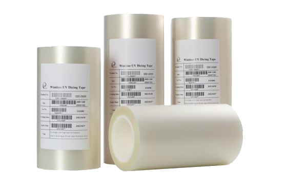
From Ceramic Substrates to Precision Alloys: How to Select Dicing Blades for Your Application
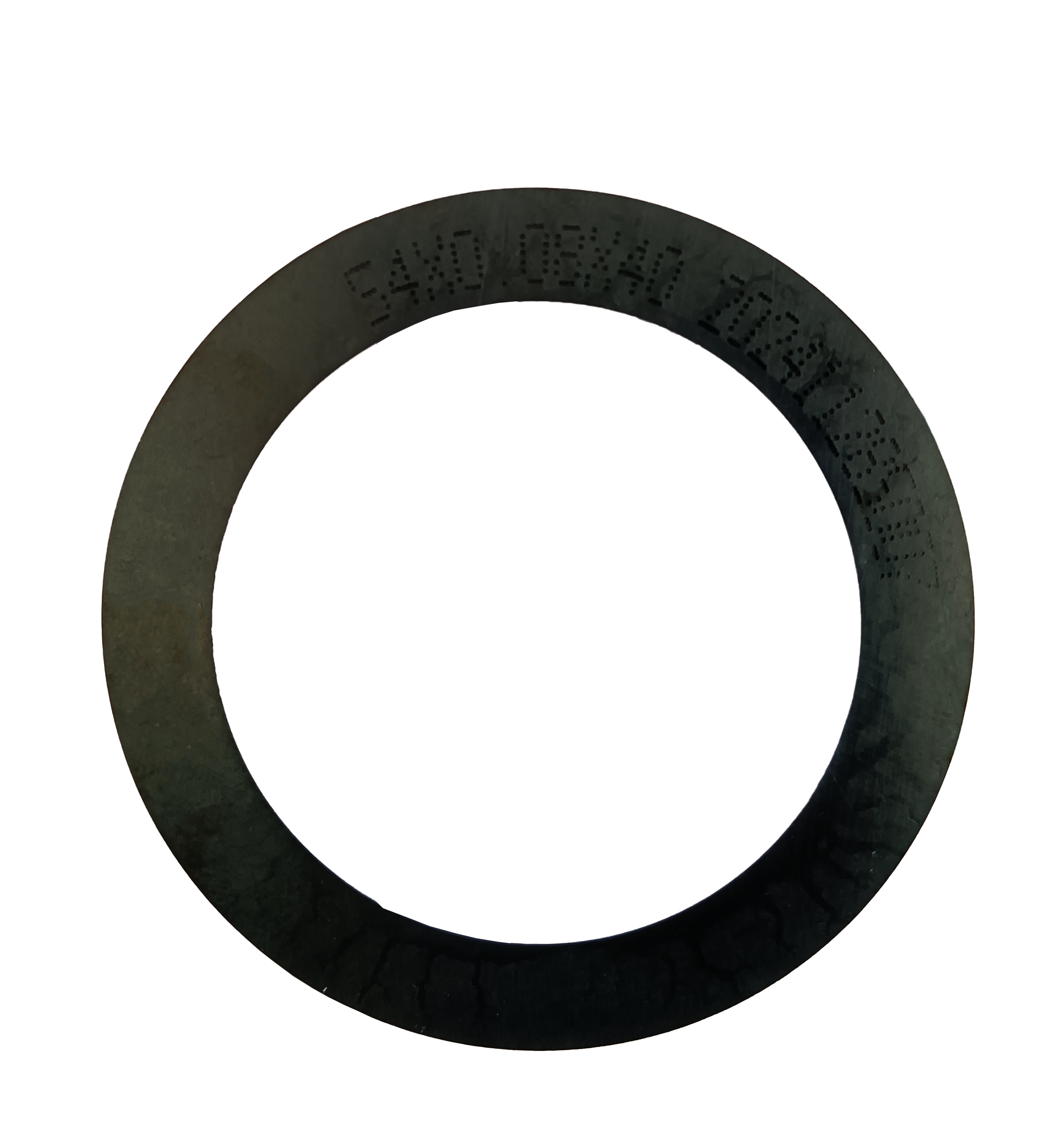
A dicing blade is not a universal consumable. The blade geometry that produces a clean cut on a silicon wafer can chip a ceramic substrate, load up on a ductile alloy, or leave micro-damage on an optical component. Selection therefore starts with the application — the workpiece material, the cutting environment and the quality definition — and only then moves to specifications such as bond type, blade thickness, diamond grain size and blade body design.
This guide maps dicing blade requirements across the cutting environments that dominate precision manufacturing: semiconductor wafer dicing, ceramic substrate cutting, optical device cutting and precision alloy component cutting. For each one, it shows which blade attributes carry the most weight, how those attributes connect to operating conditions such as anti-static setups and high-speed spindle cutting, and where low chipping has to be engineered into the specification rather than inspected out at the end of the line.
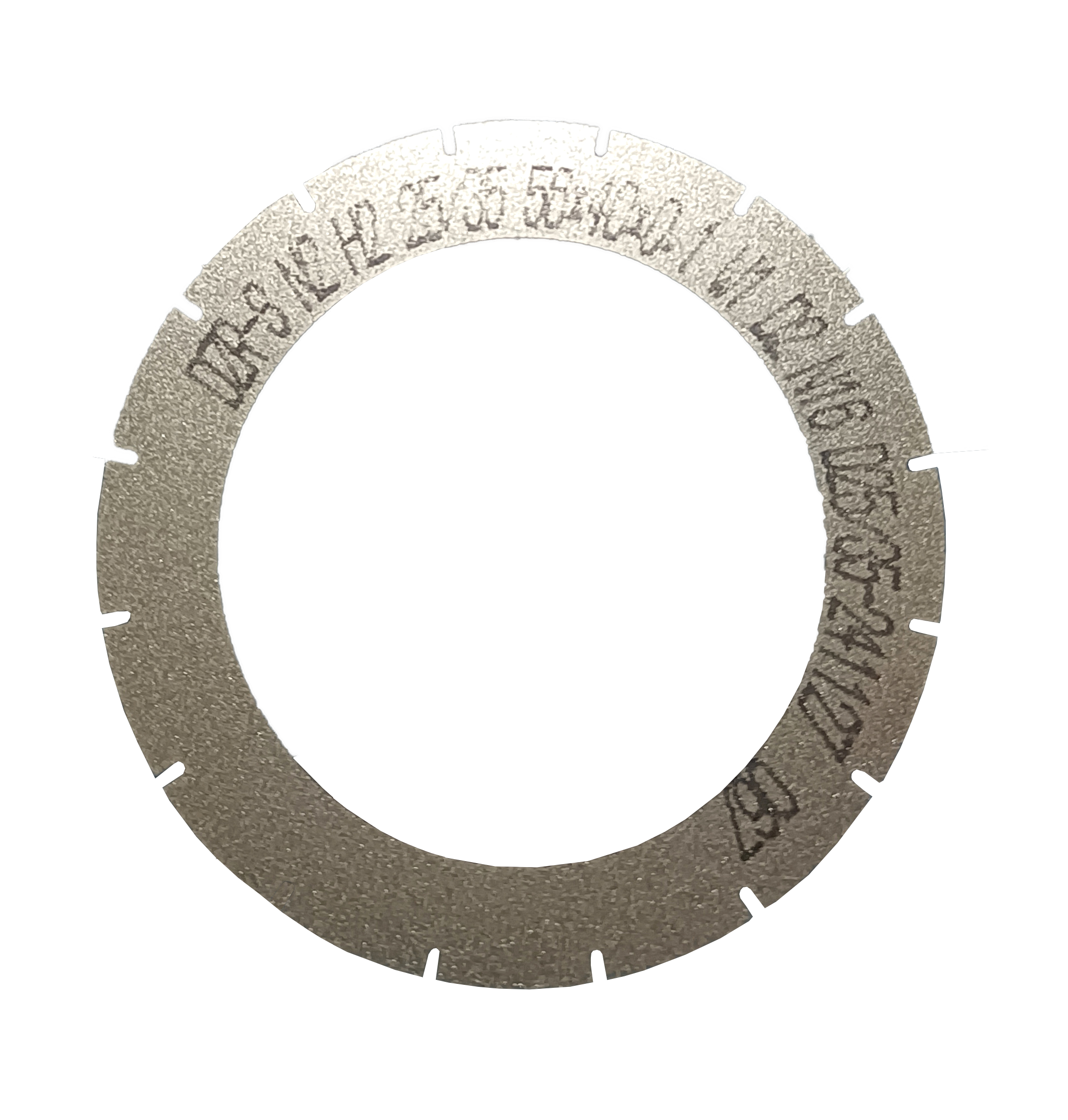
WINTIME Semiconductor Technology Co., Ltd., established in 2020, integrates the research, development, production and sales of high-precision wafer-level cutting blades, and supplies cutting blades, cutting tapes and cutting solutions. Its range includes the DZY Series Wafer Dicing Blade, the DZR Series Dicing Blade and the DZR-S Series Slotted Dicing Blade, together with hubbed, hubless, flanged and serrated designs produced in metal-bond and resin-bond diamond constructions.
Why One Blade Specification Rarely Fits Every Application
Dicing blade selection is a matching problem, because material removal behaves differently in each material class. How the diamond edge behaves depends on whether the workpiece is hard and brittle, brittle and optically sensitive, or ductile and heat-generating. A specification that performs well in one of those environments can create rejects in another.
- Ceramic substrate cutting. Hard, brittle workpieces generally fail by chipping and edge fracture. The acceptance criteria are usually chipping tolerance, kerf width and dimensional stability rather than cutting speed alone.
- Optical device cutting. The risk is micro-damage and contamination on a surface that cannot be reworked. Low chipping and precise dimensional control become the primary quality requirements.
- Precision alloy component cutting. Ductile material tends to load the abrasive and generate heat, so wear resistance, low cutting loss and stable dimensional control across long production runs matter most.
- Semiconductor wafer dicing. Ultra-thin wafers and high-value substrates combine several of these risks at once, which is why blade thickness control and static control are treated as process-critical rather than secondary.
The cutting environment is the second variable. Blades in this category are designed for Class 100/1000 clean room conditions with constant temperature (22±2 °C), constant humidity (45%–55%), dust-free and anti-static conditions, and a high-speed spindle environment. The cutting operation itself involves high-speed spindle rotating cutting, dry or wet cutting, automatic dicing machine continuous operation and precision feeding cutting. A blade that suits the material but not the environment will still underperform.
Four questions to answer before specifying a blade:
- What is the workpiece material, and how does it fail — chipping, cracking, loading or dimensional drift?
- Which quality metric is actually measured at the end of the line — chipping size, kerf width or dimensional accuracy?
- What are the machine and environment conditions — spindle type, feed mode, dry or wet cutting, clean room class, static control?
- What production volume and blade life must the process sustain before a blade change is acceptable?
What the Market Data Says About Application-Led Blade Selection
The global dicing blade market was valued at USD 1.31 billion in 2024, with projections to reach USD 1.84 billion by 2034 (Intel Market Research). That growth is not concentrated in a single substrate. Diamond-embedded dicing blades accounted for more than 60% of total market share as of 2025, largely because of their performance in cutting silicon carbide (SiC) and gallium nitride (GaN), while resin bond blades held an estimated 42% share of the dicing blade market in 2024, equivalent to USD 183.6 million.
Several technical trends reinforce the same direction. Hubless dicing blades are increasingly preferred for 300 mm wafer processing because of superior stability and reduced runout compared with hubbed blades. Standard outer diameters for semiconductor wafer dicing blades are 55.56 mm (2.187 inches) and 76.2 mm (3.0 inches), and for bare silicon dicing the industry standard diamond grit range is 2 to 6 microns (#2000 to #4000 grit) in order to minimize chipping. Regionally, China's exports of cutting blades to Vietnam grew by USD 18 million between 2024 and 2025, according to the Observatory of Economic Complexity, which points to expanding regional demand for semiconductor tooling.
Two practical conclusions follow for buyers. First, a single blade specification can no longer serve a mixed production floor; blade portfolios now have to cover hard brittle materials, optical materials and ductile metals. Second, the design trends that matter most — thinner blades, hubless bodies, tighter grit control — are all application-driven, which means the specification has to be derived from the cut, not from a catalogue page.
The Five Variables That Decide Application Fit
Across the applications covered in this guide, five variables carry most of the selection weight. Each one can be matched to a specific operating requirement rather than chosen by habit.
| Selection variable | What it controls | Options and reference points |
|---|---|---|
| Bond system | How the diamond abrasive is retained and how the cutting edge renews itself during wear | Metal bond for metal dicing blades; resin bond for resin dicing blades |
| Blade thickness | Kerf width, material loss and the minimum feature size the process can cut | From ultra-thin ≤9 μm through to standard specifications |
| Diamond abrasive grain size and concentration | Edge behaviour and chipping tendency at the cut surface | Customizable; the industry reference for bare silicon dicing is 2–6 microns (#2000–#4000 grit) |
| Blade body design | Mounting, stiffness and runout behaviour on the spindle | Hubbed, hubless, flanged, serrated and slotted (DZR-S Series Slotted Dicing Blade) designs |
| Coating and static control | Particle and electrostatic management in clean room cutting | Anti-static and wear-resistant coating options |
Note that thickness is a system decision, not an isolated one. A blade thickness of 9 microns or less reduces kerf and material loss, but it also changes how the blade behaves under spindle load — which is why thin blades are normally specified together with the dicing machine, the spindle and the tape mounting process rather than on their own.
Mapping Blade Requirements by Application
Ceramic Substrate Cutting: Hard, Brittle and Unforgiving at the Edge
Ceramic substrate cutting is a chipping-control problem first and a throughput problem second. Blades specified for this environment are designed for ceramic substrate cutting conditions and are used across functional ceramics, where the process goal is high-precision cutting with narrow kerf, low chipping and stable dimensional control. Because the workpiece is hard and brittle, the specification has to balance an abrasive that stays sharp against a bond that does not shed prematurely.
Practical selection points for ceramic work:
- Confirm the thickness against the required kerf and the number of cuts per panel, since kerf and material loss accumulate differently on brittle materials.
- Confirm the grain size against the permitted chipping limit before committing to a production order.
- Verify the blade body design against the dicing machine and spindle interface in use, especially where cut quality depends on runout behaviour.
- Validate with a test cut on production-representative material, because ceramic failure modes appear at the exit edge rather than in the middle of the cut.
Optical Device Cutting: Micro-Damage and Contamination Control
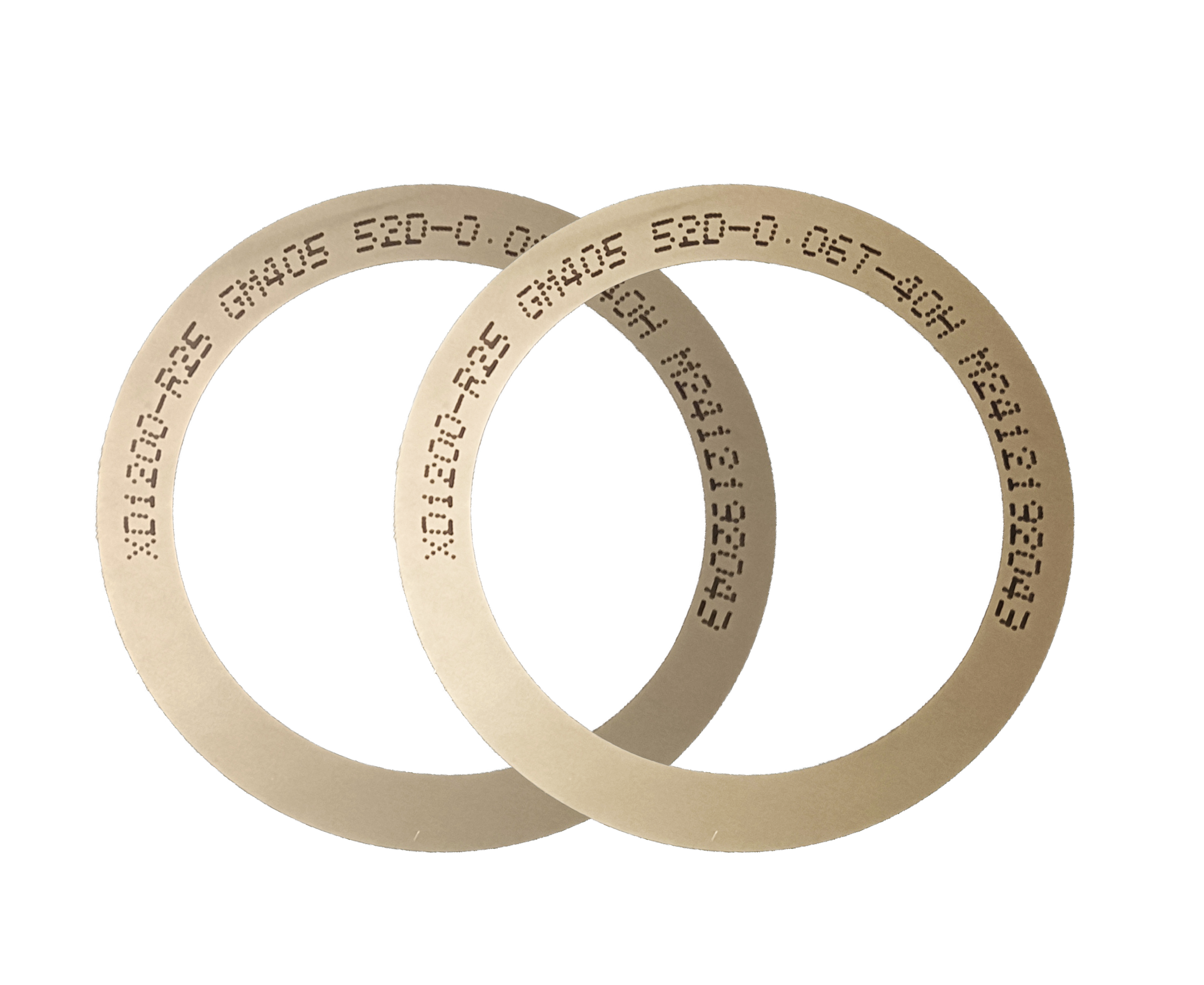
Optical device cutting shifts the priority from edge strength to surface integrity. These blades are applied in optical device cutting projects within the optical communication industry, where the process function is high-precision cutting with low chipping and stable dimensional control on materials that include optical glass. Because the finished surface usually cannot be reworked, damage introduced at the cut propagates into the component rather than being removed downstream.
Three requirements tend to dominate in this environment. First, chipping behaviour has to be controlled at a level the optical inspection step can accept. Second, the blade has to run without generating contamination that would compromise the surface. Third, dimensional control must remain stable across the run, since optical components are frequently assembled to tight tolerances. Clean room conditions, constant temperature and constant humidity, and anti-static operation all support those requirements and are part of the specified operating environment rather than optional extras.
Precision Alloy Component Cutting: Ductility, Heat and Wear
Precision alloy component cutting behaves differently again. Ductile material tends to load the abrasive, raise heat at the contact zone and change effective sharpness during a cut, so the specification priorities are wear resistance, low cutting loss and long service life under continuous operation. Blades used in this application are applied to alloy materials and precision alloy component cutting projects, and are typically run in dry or wet cutting mode on automatic dicing machines with precision feeding.
For alloy work, the selection conversation should cover:
- Bond system and grain combination, matched to the alloy family and the required balance between material removal and edge retention.
- Cooling and cutting mode, because the dry or wet decision affects both heat generation and blade wear rate.
- Wear behaviour over a full production shift rather than a single test cut, since ductile-material wear is progressive.
- Dimensional stability across the run, so that kerf and component dimensions stay inside tolerance without operator intervention.
Metal-bond diamond constructions — including electroformed hard dicing blade types — are commonly used where wear resistance and blade life dominate the decision, while thinner and finer-grain specifications are used where kerf and chipping limits are the tighter constraint.
Semiconductor Wafer Dicing: The Baseline Reference Case
Semiconductor wafer dicing sits at the most demanding end of the range and works well as a baseline for comparison. Here the requirements combine ultra-thin blade thickness of 9 microns or less with high dimensional accuracy, anti-static operation and stability in mass production. This is the environment where the DZY Series Wafer Dicing Blade and hubless Dicing Blade designs are typically specified, including for 8-inch and 12-inch ultra-thin wafer precision dicing and for high-value semiconductor substrate cutting such as SiC/GaN, ceramic and optical glass.
Hubless designs are increasingly preferred for 300 mm wafer processing because they offer superior stability and reduced runout compared with hubbed blades. For buyers mapping an application for the first time, the wafer case is useful because it makes the thickness-versus-rigidity trade-off explicit: the thinner the blade, the more the surrounding process — spindle, feed, tape and static control — has to compensate.
A Six-Step Selection Workflow for a New Application
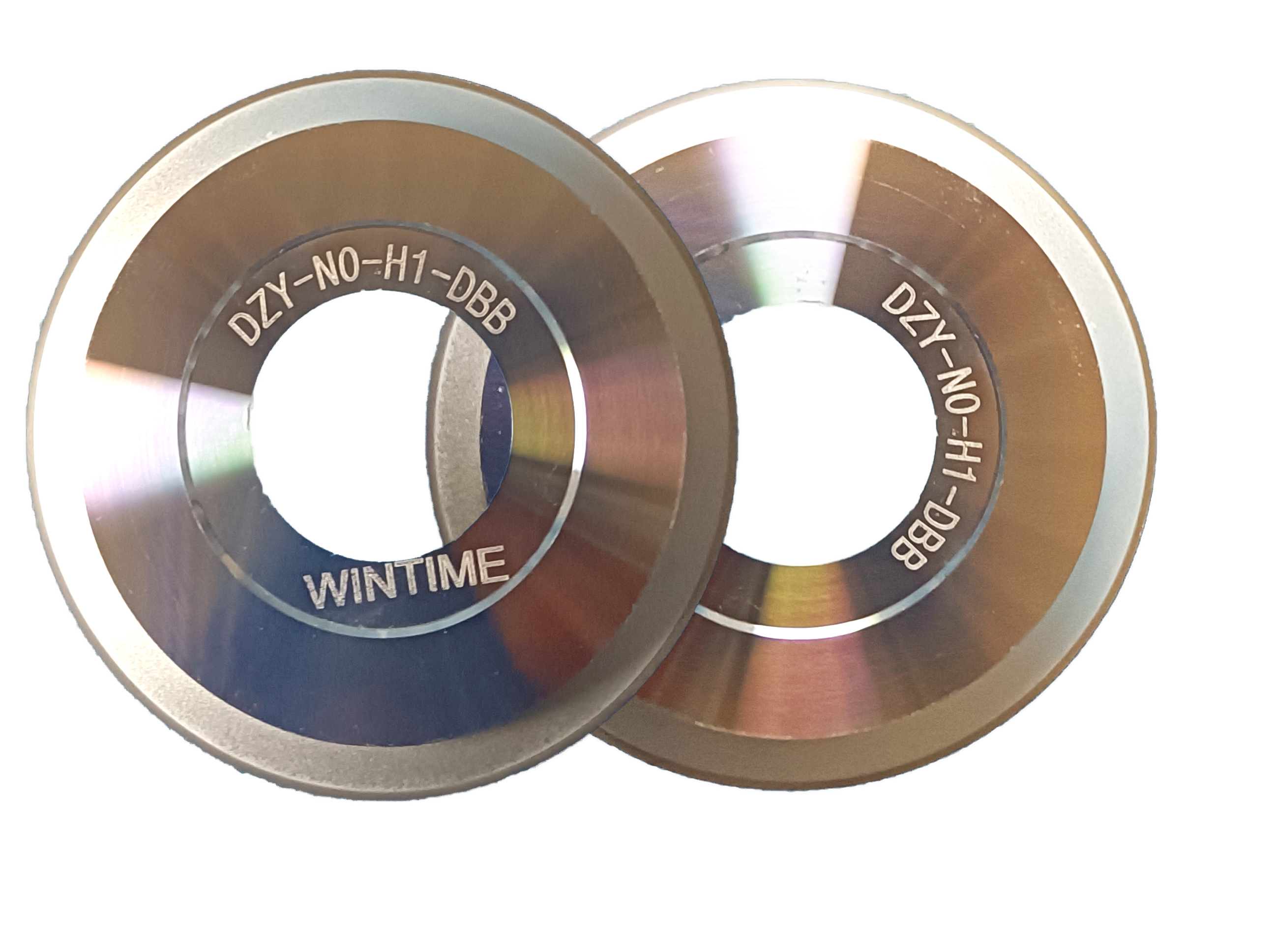
The workflow below converts the application mapping above into a repeatable sequence that can be used for ceramic, optical, alloy or wafer projects alike.
Step 1 — Define the workpiece and the failure mode. Record the material, the component geometry and the way rejects actually occur. Ceramic work generally fails at the edge, optical work fails at the surface, and alloy work fails progressively through wear and dimensional drift.
Step 2 — Choose the bond system. Metal bond and resin bond are both available and behave differently in wear and edge renewal. The bond decision should follow the material class and the required blade life, not the price of the blade alone.
Step 3 — Set the thickness against the kerf budget. Thickness ranges from ultra-thin specifications of 9 μm or less up to standard dimensions, and it directly determines kerf and material loss. Confirm the target kerf and the permitted cut loss before locking the thickness.
Step 4 — Match abrasive grain size and concentration to the chipping limit. Grain size and concentration are customizable parameters. As a reference point, bare silicon dicing typically uses a 2–6 micron range (#2000–#4000 grit) to minimize chipping, and comparable logic applies when translating a chipping tolerance into a grain specification for other materials.
Step 5 — Match the blade body design to the machine. Hubbed, hubless, flanged, serrated and slotted designs mount and behave differently on the spindle. Confirm the outer diameter, inner diameter and overall dimensions against the automatic wafer dicing machine and the spindle actually in use.
Step 6 — Confirm the environment, then validate and scale. Check the clean room class, temperature and humidity band, static control and dry or wet cutting mode. Then validate the specification through a simulated cutting test and dimension and surface inspection before moving to serial production with defined quality control.
Use Cases: How the Mapping Performs in Production
A documented case illustrates what application-matched specification delivers over time. A semiconductor packaging factory in China uses WINTIME blades for high-precision dicing of 8–12 inch semiconductor wafers for chip packaging, with an annual usage of more than 500,000 pieces and mass production line matching. Over a three-year period, the reported results were a cutting chipping rate of 5 μm or less, a 12% increase in wafer yield, and stable mass production without blade replacement. The performance factors behind that result were the ultra-thin thickness of 9 μm or less, narrow kerf, low material loss and long service life.
The same logic transfers across application types. In ceramic substrate cutting, the decisive attributes are chipping control and kerf stability. In optical device cutting, they are surface integrity and dimensional consistency under clean room conditions. In precision alloy component cutting, they are wear resistance and cutting loss. In each case the specification is derived from the failure mode the buyer is trying to prevent — which is why two buyers cutting the same nominal material can legitimately need different blades.
Comparison Tables for Shortlisting
The first comparison addresses bond selection. The second maps application environments to the blade attributes that should be confirmed before quotation.
| Comparison dimension | Metal-bond dicing blade | Resin-bond dicing blade |
|---|---|---|
| Bond material | Metal bond | Resin bond |
| Abrasive | Diamond abrasive grains (core functional material) | Diamond abrasive grains (core functional material) |
| Reported market share, 2024 | Not separately reported in the cited source | Estimated 42% of the dicing blade market (USD 183.6 million) |
| Customizable parameters | Thickness, grain size and concentration, dimensions, coating | Thickness, grain size and concentration, dimensions, coating |
| Typical selection emphasis | Wear resistance, blade life and edge stability on hard or ductile materials | Fine cutting behaviour and chipping control where surface quality dominates |
| Application | Operating environment | Blade attributes to confirm |
|---|---|---|
| Ceramic substrate cutting | Designed for ceramic substrate cutting environments; clean room and high-speed spindle operation | Bond system, thickness, grain size, blade body design, chipping tolerance |
| Optical device cutting | Optical device cutting projects in optical communication; dust-free, anti-static, controlled temperature and humidity | Chipping behaviour, dimensional accuracy, contamination control, blade runout |
| Precision alloy component cutting | Alloy materials processed in dry or wet cutting mode on automatic dicing machines | Wear resistance, cutting loss, service life, dimensional stability |
| Semiconductor wafer dicing | Class 100/1000 clean room, 22±2 °C, 45%–55% humidity, anti-static, high-speed spindle | Ultra-thin thickness ≤9 μm, grain size (2–6 μm reference for bare silicon), hubless or hubbed body design |
FAQ: Application-Fit Questions Buyers Ask
1. Do dicing blades for ceramic, optical and alloy cutting require special operating conditions?
Yes. WINTIME blades for these applications operate under anti-static conditions and are designed for Class 100/1000 clean room environments with constant temperature (22±2 °C), constant humidity (45%–55%), dust-free conditions and a high-speed spindle setup. The blade is designed for ceramic substrate cutting environments and applied across wafer dicing and scribing, semiconductor package cutting, ultra-thin wafer processing, optical device cutting, ceramic substrate cutting and precision alloy component cutting projects. Buyers should confirm that their clean room class, temperature and humidity band, static control and cutting mode match the specified operating conditions before qualification.
2. Can a dicing blade be customized for a specific application rather than bought as a standard item?
Yes. WINTIME works in OEM, ODM and customized production modes and can customize the bond type, abrasive size, blade thickness and dimensional specifications. The customizable parameters include blade thickness from ultra-thin 9 μm or less up to standard specifications; diamond abrasive grain size and concentration; bond type (resin bond or metal bond); outer diameter, inner diameter and overall dimensions; coating such as anti-static and wear-resistant options; cutting performance parameters such as chipping rate and service life; and packaging and labelling. Standard and customized models span the DZY Series Wafer Dicing Blade, the DZR Series Dicing Blade, the DZR-S Series Slotted Dicing Blade, and hubbed, hubless, flanged and serrated diamond dicing blade designs.
3. What drives the cost of a dicing blade for a given application?
Cost in this category is driven mainly by specification and order structure rather than by a single list price. The variables that move cost are the bond type, the diamond grain size and concentration, the thickness and dimensional tolerance, coating requirements, and the degree of customization. Order structure matters as well: the minimum order quantity is 100 pieces for standard products and 500 pieces for customized products, with negotiation possible for bulk orders. Buyers should also weigh total cost per cut rather than unit price alone, because blade life and chipping rate affect yield and blade-change frequency — the documented semiconductor packaging case, where a chipping rate of 5 μm or less and stable mass production without blade replacement were achieved over three years, is a useful reference for how those factors interact.
4. How can a buyer validate a blade specification before committing to serial production?
Validation at WINTIME is supported by defined quality control methods: dimensional precision inspection using a laser micrometer and optical projector; abrasive grain uniformity detection through microscope analysis; wear resistance and service life testing via simulated cutting test; and surface roughness and flatness inspection. After-sales support includes professional technical consultation and on-site application guidance, customized solution design for special cutting scenarios, spare parts supply and long-term technical support, with after-sales feedback response within 24 hours on working days, plus quality tracking and product optimization suggestions for mass production users. The practical sequence is to define the failure mode, run a simulated cutting test against the actual quality metric, and confirm dimensional and surface results before scaling.
5. What are the lead times and order quantities for standard versus customized dicing blades?
Standard models ship in 3–7 working days. Customized orders take 15–30 working days, depending on customization complexity and order quantity. Minimum order quantities are 100 pieces for standard products and 500 pieces for customized products, negotiable for bulk orders. For an application-specific recommendation, buyers can send the workpiece material, target kerf and chipping tolerance, required blade thickness, spindle and dicing machine details, and planned monthly volume to WINTIME at shenxiangfei@ntwintime.com, or request a quote directly through WhatsApp at +8618888053207.
Conclusion: Match the Blade to the Cut, Then Scale
Dicing blade selection is decided by the application, not by the catalogue. Ceramic substrate cutting rewards chipping control and kerf stability, optical device cutting rewards surface integrity and dimensional consistency in a clean room environment, precision alloy component cutting rewards wear resistance and low cutting loss, and semiconductor wafer dicing rewards ultra-thin thickness, grain control and static management. The five variables — bond system, thickness, grain size and concentration, blade body design, and coating and static control — provide a consistent framework for converting those requirements into an orderable specification.
WINTIME Semiconductor Technology Co., Ltd. manufactures dicing blades for these environments from a 34,000 m² facility with 100 employees, including a 35-engineer R&D team, and an annual production capacity of more than 1 million pieces, exporting to markets across Southeast Asia, East Asia, North America and Europe. Its ultra-thin wafer dicing blade project has achieved a process thickness of less than 9 microns, and the company holds two patent technologies. Customized bond type, abrasive size, blade thickness and dimensional specifications are available for buyers whose application does not fit a standard model.

Next step: match a blade to your cutting application
Share your workpiece material, target kerf and chipping tolerance, required blade thickness, spindle and dicing machine setup, and production volume. WINTIME can recommend a blade body design, bond type and grain specification for the application, and quote against standard or customized requirements.
Request a sample evaluation, quotation or application consultation:
- Email: shenxiangfei@ntwintime.com
- Tel: +86 13851530812
- WhatsApp: +8618888053207 — start a WhatsApp inquiry
- Address: No. 868, Fushou East Road, Rugao City, Jiangsu Province
Download the full product brochure: WINTIME Dicing Blade Brochure (PDF). More product information is available at en.wintime.net.cn.