
From Wafer to Die: How a Dicing Blade Works in Semiconductor Precision Cutting
A dicing blade is the consumable that converts a finished wafer into individual dies. It is an ultra-thin circular abrasive disc — diamond grit held inside a bond matrix — mounted on a high-speed spindle and fed along the streets between circuits. The cut is measured in microns, yet it sets material loss, die strength, yield, and the running cost of an entire dicing line. This explainer follows the blade through the whole process: what it is made of, what happens at the point of cut, the cleanroom environment it must survive, how a cut is set up step by step, and how an ultra-thin diamond blade compares with conventional resin-bonded alternatives.
1. Problem Definition: Why Wafer Singulation Is a Tolerance Problem
Every wafer leaves the fab carrying its full value, and singulation is the last operation that can destroy it. The saw street is the only area the circuit designer has already given up, so its width is a fixed budget. Whatever the blade removes beyond the minimum is material that has already been paid for and must now be thrown away.
Kerf width is therefore the first economic variable in dicing. A wider cut wastes active area, limits how many dies fit on a wafer, and on thin wafers also weakens the die edge. The second variable is chipping: micro-cracks that travel in from the cut edge and later appear as die breakage or field failures. The third is dimensional stability — if kerf drifts as the blade wears, the street design must accommodate the widest cut the blade will ever produce, not the cut it produces when new.
A fourth constraint is operational. Dicing machines in mass production run continuously and unattended. A blade that loads, glazes, or breaks a hub stops the line, and the recovery cost of a stopped dicing tool is far higher than the price difference between two blades.
The practical problem for a semiconductor, optical, or ceramic manufacturer is therefore not which blade is sharpest. It is which blade holds kerf, chipping, and dimensional accuracy inside specification for a whole production run, on the buyer's material, at the buyer's spindle load, without adding process steps.
2. Industry Background: Where the Dicing Blade Market Stands
The dicing blade is a small consumable attached to a large installed base. Intel Market Research values the global dicing blade market at USD 1.31 billion in 2024, with projections to reach USD 1.84 billion by 2034.
Blade type shapes how that market behaves. Diamond-embedded dicing blades account for over 60% of total market share, a position the Wafer Dicing Blade Market Outlook attributes to their performance in cutting silicon carbide (SiC) and gallium nitride (GaN). Resin-bond blades remain a large segment: an estimated 42% share, or USD 183.6 million, in 2024. That split explains why many procurement comparisons end up being a bond-type decision rather than a brand decision.
Competition is concentrated. DISCO Corporation holds an estimated 52–55% global share of dicing equipment and associated precision blades, which means blade supply and machine platforms are unusually interlinked.
Two structural shifts are visible in the data. First, hubless dicing blades are increasingly preferred for 300 mm wafer processing because of superior stability and reduced runout compared with hubbed blades. Second, supply is moving regionally: according to the Observatory of Economic Complexity, China's exports of cutting blades to Vietnam grew by USD 18 million between 2024 and 2025.
Published market sizing should be read with care. Estimates differ by scope — some sources count only blade revenue, others include equipment-linked consumables and wider manufacturing value chain. For procurement purposes the useful conclusion is directional: demand is growing, diamond-embedded designs dominate high-value cutting, and hubless configurations are the direction of 300 mm processing.
3. How a Dicing Blade Works: Anatomy and Cutting Mechanics
3.1 What the blade is made of
A dicing blade has three functional parts: the abrasive, the bond, and the body.
- The abrasive is diamond. For bare silicon dicing, the industry standard grit size range is 2 to 6 microns (#2000 to #4000 grit), fine enough to keep chipping small. Coarser grit removes material faster but leaves a rougher edge.
- The bond holds the grit and controls how the blade wears. Resin bonds are the traditional choice and still hold a large share of the market; metal and electroformed bonds are used where wear resistance and edge retention matter more. Bond behaviour, not diamond alone, decides whether the blade self-sharpens smoothly or glazes.
- The body defines the geometry. Standard outer diameters (OD) for semiconductor wafer dicing blades are 55.56 mm (2.187 in) and 76.2 mm (3.0 in). A hubbed blade carries a hub that is clamped by the machine flange; a hubless blade is a thin ring mounted and tensioned differently. Hubless designs are increasingly preferred for 300 mm wafers because they reduce runout and improve stability at the cut.
Blade thickness and the exposed depth of diamond below the flange set the minimum kerf the process can achieve. That is the single most important geometric relationship in wafer dicing: thinner blade, narrower cut, more usable die area.
3.2 What happens at the point of cut
Cutting is grinding, not sawing. The blade is rotated at high speed by a precision spindle and the wafer is indexed along the street; material is removed by thousands of diamond points passing across the surface at the blade periphery. Removal is brittle — silicon and ceramics fracture at a small scale — and cut quality depends on keeping that fracture zone narrow and shallow.
Two mechanisms keep the blade working. First, the bond wears back behind the diamond so fresh, sharp grit is continuously exposed; this self-sharpening behaviour is what separates a stable blade from one that glazes. If the bond wears too slowly, the diamond flattens; if it wears too quickly, the blade loses exposure and kerf grows.
Second, coolant manages heat. In wet cutting, deionised water is directed at the cut to remove heat and flush debris. Dry cutting is used where the material or the process makes coolant impractical. Heat is a first-order concern at the blade tip because temperature drives bond wear and can push the blade off its dimensional target.
The variables a process engineer actually controls are spindle speed, feed rate, blade exposure, depth per pass, number of passes, coolant flow, and the choice between single-pass and step cutting. These parameters set the balance between throughput, chipping, and blade life — and they explain why a blade cannot be evaluated from a datasheet alone, because the same blade behaves differently at different feeds.
3.3 The operating environment the blade must hold
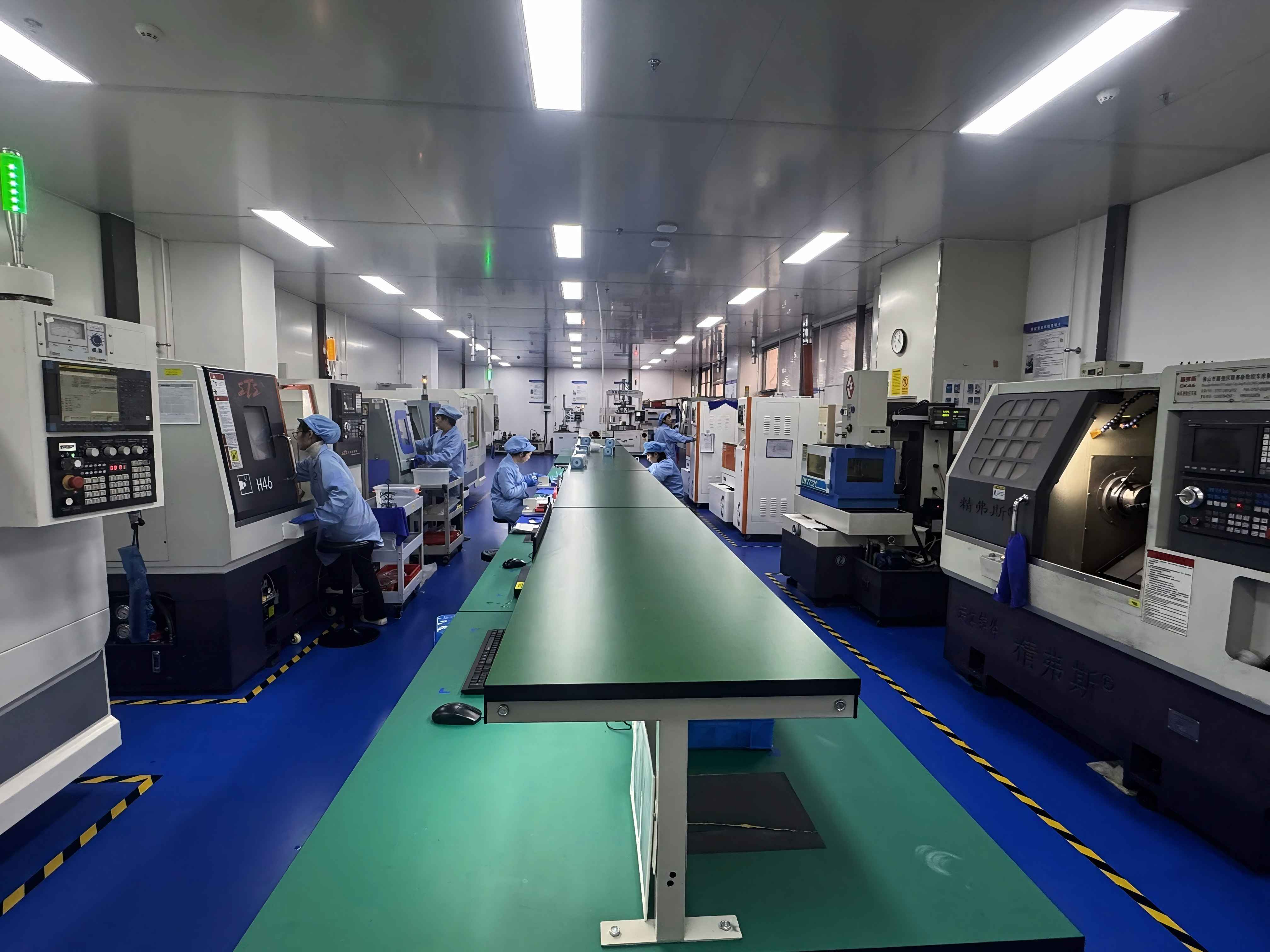
Wafer dicing happens inside a controlled environment, and the blade is part of what that environment protects. High-precision dicing areas operate as Class 100/1000 cleanrooms with temperature held at 22 ± 2 °C and relative humidity controlled between 45% and 55%, with dust-free and anti-static control throughout.
- Temperature: thermal drift in the spindle and structure changes the effective depth of cut and blade position at the micron level.
- Humidity: the expansion and adhesion of the mounting tape change with moisture, and static charge builds more easily in dry air. Static discharge near a cut edge is a yield risk in its own right.
- Particles: debris in the cutting zone is a direct defect source on an exposed die surface.
- Machine behaviour: automatic dicing machines run continuous, repetitive cycles. Blades are specified on the assumption of uninterrupted production, so anything that forces a stop — loading, glazing, hub damage — appears as lost capacity rather than as a blade cost.
This is why anti-static blade designs and cleanroom-compatible blade coatings exist. They are process-environment requirements, not marketing features.
4. Detailed Solution: WINTIME's Ultra-Thin Wafer D Blade
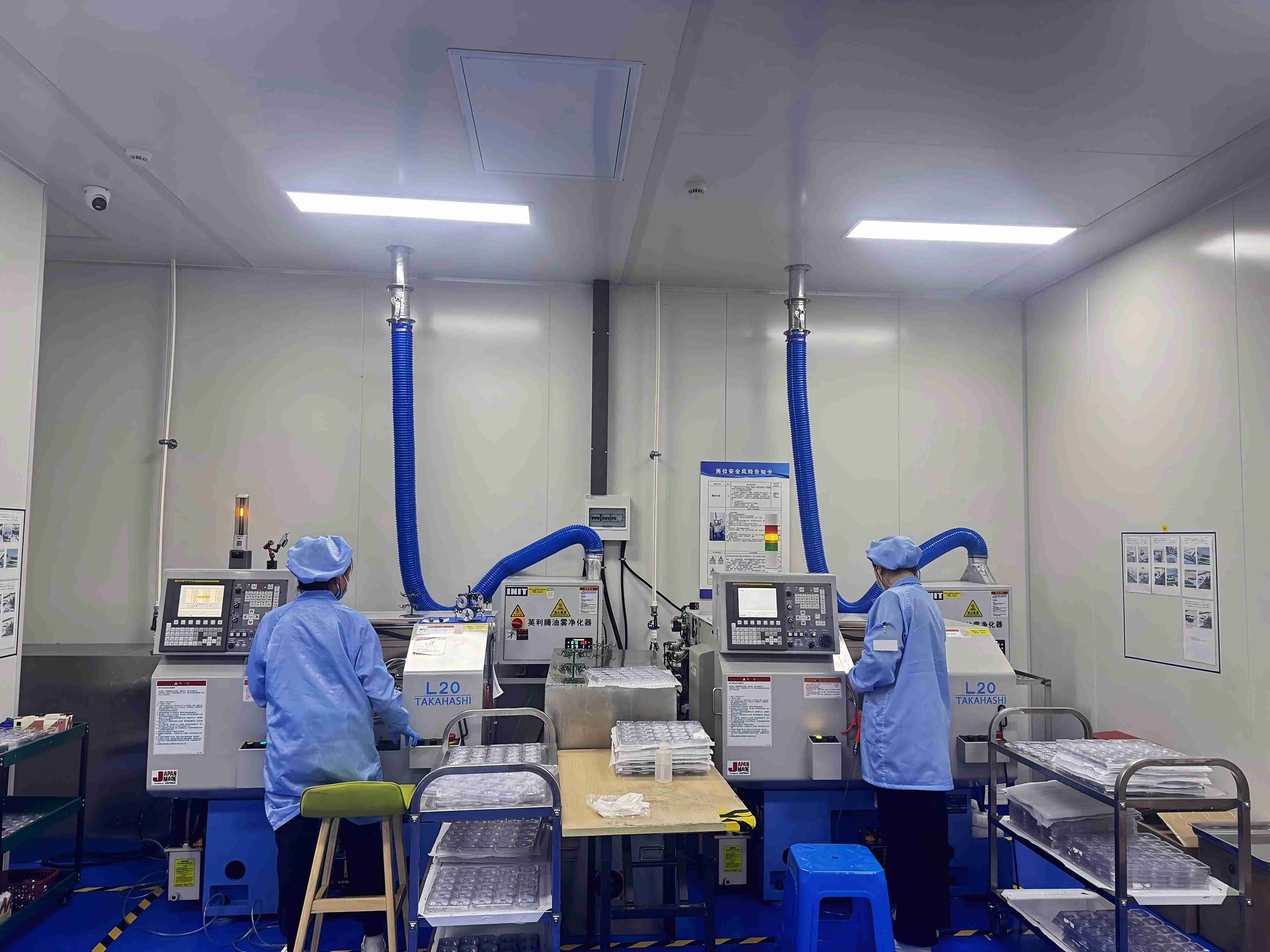
WINTIME Semiconductor Technology Co., Ltd. is a Jiangsu-based manufacturer of high-precision wafer-level cutting blades, established in 2020 and located at No. 868, Fushou East Road, Rugao City, Jiangsu Province. The company integrates research, development, production, and sales of high-precision wafer-level cutting blades, together with cutting tapes and cutting solutions. Around 30% of its sales are exported to Southeast Asia, East Asia, North America, and Europe. Its blade portfolio covers hubless and slotted configurations, including the DZY Series Wafer Dicing Blade, the DZR Series Dicing Blade, the DZR-S Series Slotted Dicing Blade, and the Electroforming Hard Dicing Blade.
Scale and capacity: the Nantong WINTIME Semiconductor Special Materials Project, launched in 2023 with a total investment of nearly tens of millions of yuan, added a factory and auxiliary buildings of 34,000 m². Annual dicing blade capacity exceeds 1 million pieces, and the company's annual output of dicing blades ranks among the top in the country. The site employs around 100 people, of whom 35 are R&D engineers. The company holds 2 patent technologies and has received awards in national, provincial, and municipal science and technology competitions.
The project most relevant to this topic is the completed Ultra-thin Wafer D Blade. The project achieved a blade thickness below 9 microns in the process, which the company describes as reaching the international cutting-edge level. WINTIME is one of the few domestic companies able to mass produce at that thickness.
4.1 What the ultra-thin design changes at the cut
- Kerf: an ultra-thin blade thickness of below 9 µm produces a 9 µm kerf width, against 12 µm for mid-range imported blades — a 25% reduction in material loss.
- Chipping: a proprietary diamond abrasive formula reduces the chipping rate to ≤5 µm, against ≤10 µm for the same comparison set — 50% lower.
- Bond structure: an optimized bond structure improves cutting stability in brittle materials such as silicon wafer and ceramic.
- Wear resistance: high wear resistance maintains dimensional stability in mass production, holding ±0.001 mm tolerance against ±0.003 mm for mid-range imported blades.
- Cleanroom compatibility: an anti-static coating design supports Class 100/1000 cleanroom operation.
- Service life: 30% longer than mid-range imported alternatives.
Best-fit applications for this blade are ultra-thin 8-inch and 12-inch wafer precision dicing; high-value substrates such as SiC, GaN, ceramic, and optical glass; mass production lines with strict requirements for yield and material utilization; Class 100/1000 cleanroom manufacturing environments; and miniature semiconductor components including MEMS and power devices.
On the machine side, the blade is compatible with standard semiconductor dicing machines and requires no equipment modification. Spindle load during cutting is 15% lower, which reduces energy consumption; processing speed is 20% higher under the same power condition; heat generation during high-speed rotation is reduced, lowering cooling-system energy use; and performance is consistent across the product lifecycle without degradation. Maintenance behaviour follows the same pattern: a longer replacement cycle reduces tool-change frequency by 30%, no additional cleaning or debugging is required, and no frequent calibration is needed in mass production.
5. Step-by-Step Breakdown: From Wafer to Singulated Die
- Prepare and mount the wafer. The wafer is mounted face-up on dicing tape stretched in a ring frame. Tape choice matters: it must hold the wafer during cutting and then release dies cleanly during expansion. Because tape behaviour is humidity-sensitive, the mounted wafer is normally stabilized in the same 22 ± 2 °C, 45–55% RH environment as the dicing tool.
- Specify the blade. Selection starts from the material and the kerf budget, then works outward: bond type, diamond grit (2–6 microns, #2000–#4000, for bare silicon), blade thickness (below 9 µm for ultra-thin wafer work), outer diameter (55.56 mm or 76.2 mm), and hub or hubless configuration. Hubless blades are increasingly the choice for 300 mm wafers.
- Mount and check runout. The blade is fitted to the spindle flange and the assembly is checked for runout before the first cut. Runout is a chipping source from the very start of the run, and it is one of the reasons hubless designs matter at 300 mm.
- Establish exposure and dress the blade. The exposed diamond depth below the flange sets the usable cutting edge. Dressing brings fresh grit to the surface and removes any glazed layer, so the blade begins the run in a known condition rather than a random one.
- Set the parameters. Spindle speed, feed rate, cut mode (single pass or step cut), depth per pass, and coolant flow are set for the material. On brittle, high-value substrates the trade is always the same: slower feed and lighter passes reduce chipping, while higher feed raises throughput and blade wear.
- Cut and monitor. The machine indexes along each street in continuous production. A stable cut shows as consistent kerf, steady spindle load, and an even edge. Rising spindle load or widening kerf are the early signals of bond loading or wear, and they should trigger a blade change before quality drifts out of specification.
- Clean, expand, and separate. After dicing, the wafer is cleaned, the tape is expanded to open the die gaps, and the dies are picked. Blade quality is finally measured here — in the chipping at the die edge and in how many dies survive pick-and-place intact.
Across all seven steps, the precondition for consistency is batch-level traceability: knowing which blade, from which production batch, cut which wafer under which parameters.
6. Use Cases: Where the Dicing Blade Decides the Outcome
- Semiconductor wafer dicing (8-inch / 12-inch). Ultra-thin wafers leave the least margin for kerf loss and edge damage, so blade thickness and bond stability dominate the result.
- SiC and GaN power devices. These substrates are hard, brittle, and expensive per wafer. Material loss and chipping both translate directly into cost, and diamond-embedded blades account for over 60% of the market precisely because of their behaviour in SiC and GaN cutting.
- Optical communication components. Edge quality influences the optical surface, so chipping and dimensional control matter as much as throughput.
- Functional ceramics. Ceramics chip easily; an optimized bond structure that keeps the blade stable in brittle materials is the deciding factor.
- MEMS and miniature components. Where the die is small, kerf is a larger proportion of the die footprint, so a narrower cut protects area directly.
- Optical glass and alloy materials. Mixed-material and hard-material shops typically run one blade family across several materials, which makes dimensional consistency across the run more important than peak performance in a single trial.

7. Comparison Table: Ultra-Thin Diamond vs. Traditional Resin-Bonded Blades
| Comparison metric | WINTIME ultra-thin diamond dicing blade | Traditional resin-bonded blade (mid-range imported) |
|---|---|---|
| Kerf width | 9 µm | 12 µm |
| Chipping rate | ≤5 µm | ≤10 µm |
| Dimensional tolerance | ±0.001 mm | ±0.003 mm |
| Material loss from kerf | 25% lower | Baseline |
| Service life | 30% longer | Baseline |
| Wafer yield | 12% higher than traditional blades | Baseline |
| Spindle load during cutting | 15% lower (reduced energy consumption) | Baseline |
| Processing speed (same power) | 20% faster | Baseline |
| Tool change frequency | 30% lower | Baseline |
| Initial purchase cost | 10–15% higher than standard blades | Lower upfront price |
| Cleanroom design feature | Anti-static coating design for Class 100/1000 compatibility | Not specified in comparison set |
| Machine compatibility | Standard semiconductor dicing machines, no equipment modification | Standard dicing machines |
Figures above are comparative performance values from WINTIME's comparison data against traditional resin-bonded dicing blades from mainstream competitors and mid-range imported alternatives. They describe relative performance, not a guaranteed result for every material, machine, or parameter set. For market context: resin-bond blades held an estimated 42% share of the dicing blade market in 2024, worth USD 183.6 million.
8. Total Cost of Ownership: Why the Cheaper Blade Is Not the Lower-Cost Blade
A higher purchase price is not the same as a higher running cost. On the comparison data, the ultra-thin diamond blade costs 10–15% more to buy than a standard blade, but offers a lower total cost of ownership through a 30% longer service life, reduced material waste, and an 8% annual reduction in production cost from reduced downtime. Blade-related downtime falls because tool changes are 30% less frequent and no additional cleaning, debugging, or frequent calibration is required.
For a decision-maker, the calculation has four lines:
- Material saved. A 25% reduction in kerf width is recovered device area on every wafer cut.
- Yield. A 50% lower chipping rate and a reported 12% yield improvement against traditional blades on high-value substrates.
- Blade consumption. A 30% longer service life reduces the number of blades consumed per thousand wafers.
- Downtime and energy. Fewer tool changes, 15% lower spindle load, and no added process steps.
Where the balance shifts back to resin-bonded blades: processes that do not demand sub-10 µm kerf, materials that are forgiving of edge chipping, and low-value or non-critical cuts where the lowest initial price is the deciding factor. Resin-bond blades held an estimated 42% of the dicing blade market in 2024 and remain a legitimate choice in those cases. The decision criterion is cost per good die, not price per blade.
9. Keeping the Cut Stable Across Batches
The failure mode buyers fear most is not a bad blade — it is an inconsistent batch. A blade that performs in qualification and drifts in mass production stops a line.
The risk itself is well defined: batch quality inconsistency that affects stable mass production at the customer end. WINTIME's control method combines three elements — standardized production process parameters and automatic production equipment to avoid manual operation errors; a batch production data tracking system that records process parameters for every batch; and comparative testing of adjacent batches to confirm that performance is consistent between them.
On the quality-management side, the company implements an ISO 9001 quality management system and follows standard operating procedures, assigns dedicated quality inspectors to track each production batch, and maintains a batch quality file that can be traced at any time, with recall of non-conforming batches if a problem occurs. Combined with cleanroom-compatible blade design and anti-static coating, this is the difference between a good sample and a repeatable supply. Buyers who want to review the full product range can do so on the WINTIME Semiconductor website.
10. FAQ: Dicing Blade Decisions in Semiconductor Production
What cleanroom and quality requirements should a wafer dicing blade meet?
Wafer dicing runs in Class 100/1000 cleanroom conditions with temperature held at 22 ± 2 °C, relative humidity between 45% and 55%, and dust-free, anti-static control. A blade intended for that environment should be compatible with it — anti-static coating design is one example — and should come from a supplier with a documented quality system. WINTIME manufactures under an ISO 9001 quality management system with standard operating procedures, dedicated quality inspectors per production batch, and batch quality files that allow full traceability and recall if needed.
How does an ultra-thin dicing blade achieve a narrower kerf with less chipping?
Three things change at once. Blade thickness drops below 9 µm, which reduces kerf width to 9 µm compared with 12 µm for mid-range imported blades. The diamond abrasive formula is designed to reduce the chipping rate, reported at ≤5 µm versus ≤10 µm. And an optimized bond structure keeps the blade stable in brittle materials such as silicon wafer and ceramic, while high wear resistance holds dimensional tolerance at ±0.001 mm versus ±0.003 mm. The result is a narrower cut with a cleaner edge, sustained across a production run.
Is an ultra-thin diamond dicing blade more expensive to run than a resin-bonded blade?
The purchase price is higher — 10–15% above a standard blade — but the running cost is lower. A 30% longer service life and reduced material waste produce a lower total cost of ownership, and reduced downtime from fewer blade replacements lowers annual production cost by about 8%. Tool change frequency falls by 30%, spindle load by 15%, and processing speed is 20% higher under the same power. Resin-bonded blades remain the better economic choice where kerf and chipping requirements are loose — they still held an estimated 42% share of the 2024 market.
Can we validate a dicing blade before committing to mass production?
Yes — and it should be done on the buyer's own material. Blade performance is defined by the interaction of blade, material, machine, and parameters, so a meaningful validation runs the candidate blade on the same wafer type, tape, and dicing machine that will be used in production, and compares kerf width, edge chipping, spindle load, and kerf drift at the start and end of the run. Those four measurements, taken on your substrate, are more informative than any figure on a datasheet. Sample and trial requests can be raised through WINTIME's contact channels.
How does supply continuity work for dicing blade procurement?
Continuity depends on capacity and traceability rather than on lead-time promises. WINTIME's annual dicing blade capacity exceeds 1 million pieces from a 34,000 m² facility in Rugao, Jiangsu Province, supported by 35 R&D engineers and a batch quality file for every production lot. Around 30% of output is exported to Southeast Asia, East Asia, North America, and Europe. For long-run programs, the practical steps are to qualify the blade on your material, agree the batch documentation you need, and confirm compatibility with your existing dicing machines. To start that process, download the WINTIME brochure or send your wafer type, target kerf, and machine model to shenxiangfei@ntwintime.com.
11. Conclusion: The Blade Is a Process Decision
A dicing blade does one thing — it separates a wafer into dies along the streets. But the way it does that determines kerf loss, edge quality, dimensional stability, machine uptime, and ultimately cost per good die. Understanding the mechanics helps: diamond grit of 2–6 microns for bare silicon, standard ODs of 55.56 mm and 76.2 mm, hubless designs for 300 mm stability, self-sharpening bonds, and a controlled 22 ± 2 °C, 45–55% RH cleanroom environment.
The decision follows from those mechanics. Where kerf and chipping are tight — ultra-thin 8-inch and 12-inch wafers, SiC and GaN, ceramic, optical glass, MEMS, and power devices — an ultra-thin diamond blade with a 9 µm kerf, ≤5 µm chipping, ±0.001 mm tolerance, and a 30% longer service life offers a lower total cost of ownership even at a 10–15% higher purchase price. Where requirements are loose, resin-bonded blades remain a rational choice.
The tie-breaker is not the datasheet. It is whether the supplier can reproduce the same blade, batch after batch, with traceable process data and a quality system behind it.

Next step: validate the blade on your own wafer
Download the WINTIME product brochure, or send your wafer type, target kerf width, and dicing machine model for a specification review or a sample request. Contact: shenxiangfei@ntwintime.com | Tel: +86 13851530812 | WhatsApp: +8618888053207
Download the WINTIME Product Brochure