
How to Produce MEMS Devices with Efficient Sawing Blade Processes
An efficient sawing blade process for MEMS and sensor fabrication rests on five controllable elements: an ultra-thin blade matched to the substrate, a spindle that holds runout tight, tape mounting that keeps the wafer flat and the streets clear, dicing parameters that are locked instead of re-tuned per lot, and a cleaning sequence that removes debris before it becomes a defect. Control all five and MEMS singulation becomes repeatable. Lose one and the loss surfaces later as edge chipping, kerf drift, die breakage, or electrical failure after packaging.
MEMS devices are rarely uniform silicon blocks. A typical MEMS flow pairs a device wafer with a cap wafer, and many structures contain thin membranes, released moving elements, or sealed cavities that behave very differently from solid silicon under mechanical load. That is why the sawing blade cannot be treated as a consumable picked at the end of the line. In MEMS production it is a process variable that determines kerf width, die edge quality, and, in the end, device yield.
This guide is written for process engineers, packaging engineers, and procurement teams who are specifying or re-validating MEMS dicing and scribing. It covers the failure logic behind MEMS singulation, the market conditions shaping blade supply, the five control points of an efficient process, a step-by-step setup sequence, material-specific use cases, and the comparison logic for selecting both the blade configuration and the supplier.
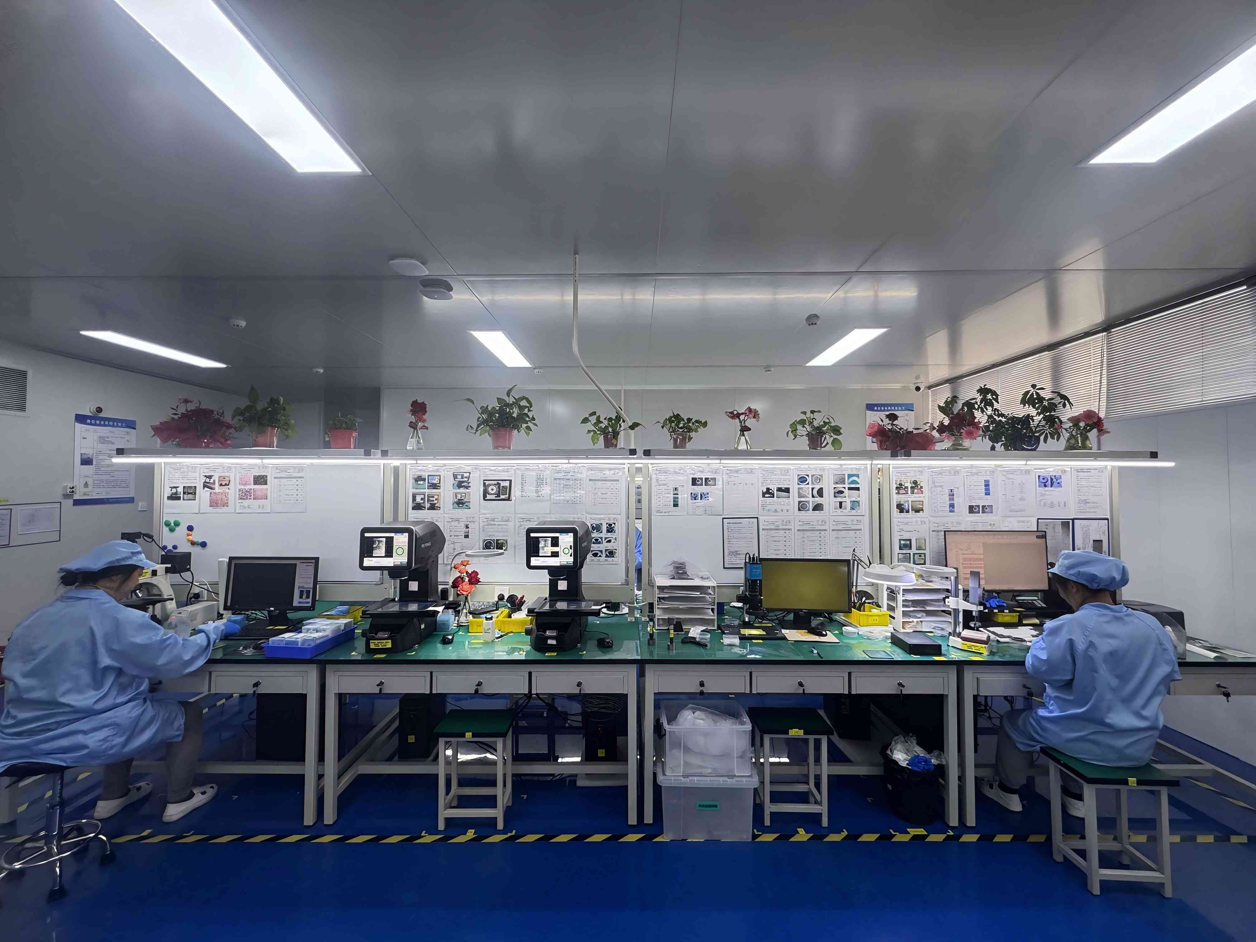
Why MEMS Singulation Fails Before the Blade Touches the Wafer
The dicing step is where accumulated process decisions are either validated or exposed. MEMS wafers carry three structural features that make singulation harder than conventional logic or memory dicing: device layers that are mechanically fragile, material stacks that mix silicon with functional layers such as ceramics, alloys, or optical films, and small die footprints that leave narrow streets with little room for kerf variation.
In practice, four failure modes account for most MEMS yield loss at the saw:
- Edge chipping and micro-cracks. Mechanical load at the blade exit side initiates cracks that may not fail the die at inspection but can propagate during thermal cycling in the field.
- Kerf drift. The cut wanders away from the street center, either because blade exposure and runout change during the run or because the wafer is not held flat.
- Tape and adhesive contamination. Inconsistent mounting leaves air pockets, local height variation, or adhesive residues that contaminate the die surface.
- Residual debris. Silicon dust and bond material left in the streets or on the die surface become defects after cleaning is skipped or under-performed.
Each failure mode traces back to a different control point — bond and blade geometry, spindle condition, tape mounting, or the cleaning sequence. The practical consequence is that there is no single universal blade for MEMS work. A blade that produces clean edges on a thin silicon sensor wafer is not automatically the right choice for a functional ceramic substrate or an optical device wafer, which is why selection has to be framed as a comparison between configurations against the actual substrate, die size, and volume.
Industry Background: A Dicing Blade Market Pushed Toward Thinner Kerfs
The economics of MEMS singulation are moving in one direction: thinner cuts, tighter streets, and more material families on the same production floor. The market data reflects that pressure.
- The global wafer dicing blade market was valued at USD 1.19 billion in 2024, with growth attributed to semiconductor miniaturization and the adoption of 300 mm wafers (Market Research Intel).
- Estimates of the same market diverge by scope rather than by direction: one research house places it at USD 1.31 billion while another places it at USD 0.437 billion, a gap that reflects whether equipment is counted alongside consumables.
- By bond type, resin bond blades held a 42% share of the dicing blade market in 2024, while metal bond blades — used for harder materials such as SiC — accounted for 33% (market.us).
- Hubless dicing blades are increasingly dominant for 300 mm wafer processing because of superior stability and reduced runout on substrates thinner than 50 µm (Semiconductor Equipment Market Data).
- Optical communication and RF/optoelectronics applications represented 16% of dicing blade market share in 2024, equal to USD 69.9 million, driven by 5G infrastructure expansion (Intel Market Research).
- On the supply side, China's exports of cutting blades to Vietnam grew by USD 18 million and to India by USD 12 million between 2024 and 2025 (OEC, Observatory of Economic Complexity).
- ISO 22180:2019 categorizes diamond tools, including sawing blades, and distinguishes CVD diamond-coated types from monocrystalline and polycrystalline types (ISO).
The wider diamond saw blade market, of which wafer dicing blades are a specialized segment, was valued at approximately USD 8.60 billion in 2025 and is projected to reach USD 10.16 billion by 2032 (Maximize Market Research).
For a MEMS line, the implication is not simply that demand is growing. It is that the substrate mix is widening while streets narrow, which shifts the qualification burden onto blade selection, spindle condition, and mounting discipline rather than onto cutting speed alone.
The Five Control Points of an Efficient Sawing Blade Process
An efficient MEMS sawing process is not defined by a single parameter but by five control points that must be specified together. Each one is a decision, and each decision carries a trade-off.
1. Blade selection: bond type, geometry, and hub configuration
The bond is what holds the diamond in place, and it dictates how the blade behaves on a given material family. Resin bond blades accounted for 42% of 2024 dicing blade market share and are widely used on silicon MEMS device wafers where mechanical load on fragile structures must stay low. Metal bond blades, at 33% share, are used for harder materials such as SiC and other difficult substrates.
Where the bond is produced by electroforming, the blade retains its form and diamond protrusion on hard, brittle functional materials — which is why an electroforming hard sawing blade is typically specified for cutting jobs where geometry retention matters more than cutting speed. A diamond sawing blade for functional ceramics follows the same logic: the abrasive has to keep cutting after the softer bond alternatives would have glazed or worn.
Blade thickness sets the kerf directly. WINTIME Semiconductor Technology Co., Ltd., a China-based manufacturer of high-precision wafer-level cutting blades, completed an ultra-thin wafer dicing blade project that achieved a blade thickness of less than 9 microns, and the company is among the few domestic manufacturers able to mass-produce at that level. For MEMS work, that matters because kerf is not only a material cost — it is die-per-wafer yield.
Hub configuration is the third dimension. A hubless sawing blade is increasingly the default for 300 mm processing and substrates thinner than 50 µm, because removing the hub reduces runout and improves stability on very thin material. A hub-type blade remains a practical option at conventional substrate thicknesses, where the flange adds rigidity and simplifies handling.
In practice, a MEMS production line usually needs more than one blade family on hand. A semiconductor wafer sawing blade for standard silicon, an optical communication sawing blade for device wafers with optical coatings, a functional ceramic sawing blade for substrates and carriers, and an alloy material sawing blade for metal components are different tools for different failure risks — not interchangeable stock.
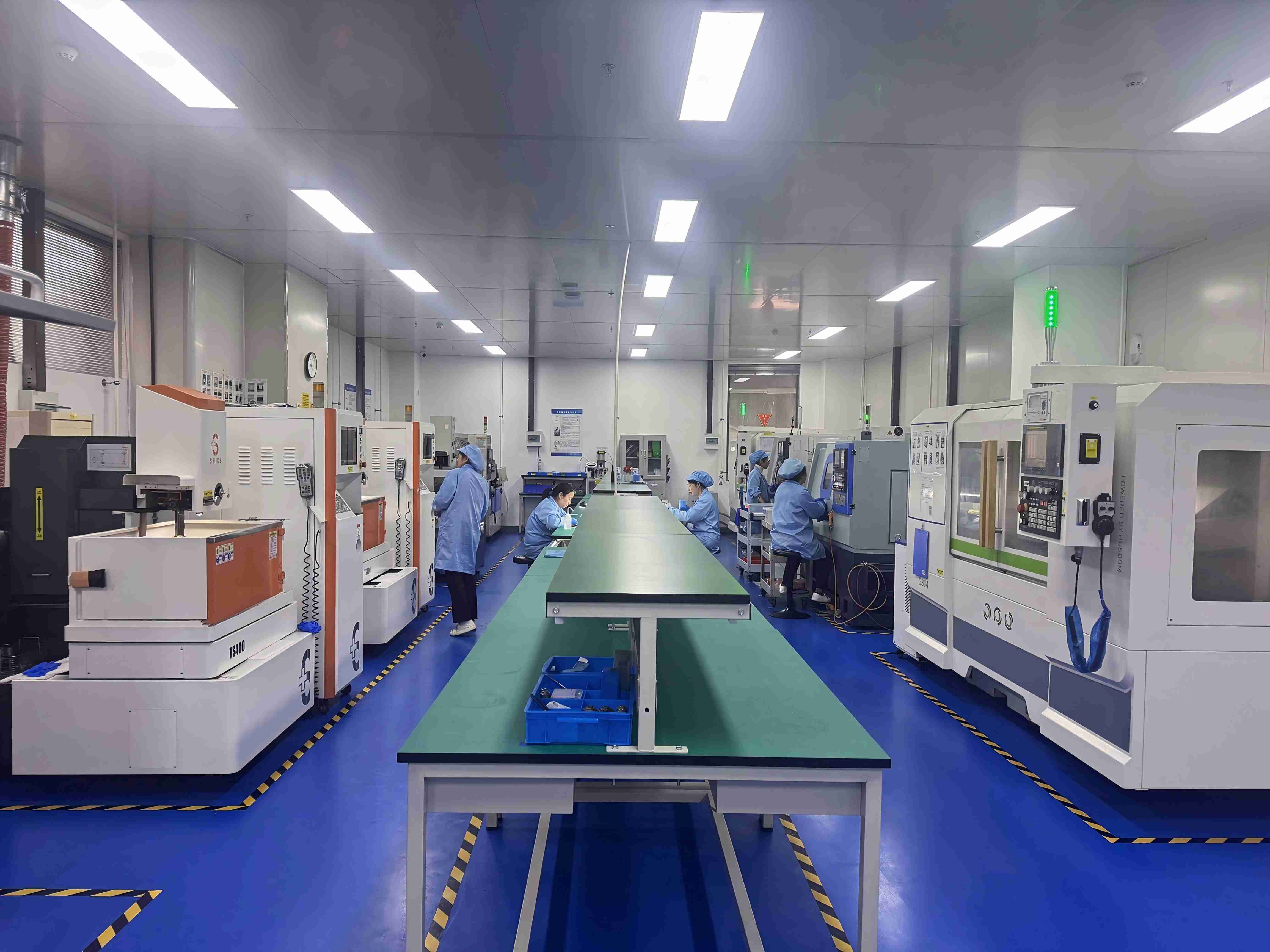
2. Spindle precision and runout control
Spindle condition is the control point most often assumed rather than measured. Radial and axial runout at the blade edge translate directly into kerf variation and edge chipping, and on thin substrates the effect is amplified. This is the mechanism behind the market shift toward hubless blades on 300 mm wafers: less runout on thinner material means fewer die edge defects.
Practical checks before a MEMS production run include verifying spindle runout against the specification used during qualification, confirming that the flange faces are clean and free of tape residue or dried slurry, checking blade exposure after mounting, and replacing worn flanges rather than re-torquing them into tolerance. Blade dressing should be treated as a scheduled step, not as a reaction to a failing cut.
3. Tape mounting: the step most often underestimated
Mounting tape is functionally part of the cutting process. It holds the wafer flat, damps vibration, and keeps the singulated die in place after the cut. When tape is applied with trapped air or uneven roller pressure, the wafer develops local height variation, and the blade effectively cuts a different depth across the same wafer — which shows up as intermittent chipping that no parameter change can fix.
A repeatable mounting procedure covers four points: inspect the wafer backside and street side for particles before mounting; apply tape with controlled, consistent roller pressure on a mounter rather than by hand; verify flatness and frame seating before the wafer enters the saw; and confirm tape type against the material being cut, since optical and functional material wafers may require different adhesion behaviour than plain silicon. WINTIME supplies cutting tapes alongside its blade range, which allows blade and tape to be qualified as a pair rather than as separate purchases.
4. Locked dicing parameters
Feed speed, spindle speed, coolant flow, and blade exposure should be established once through a parameter window trial and then locked into the recipe. Re-tuning parameters between lots is one of the most common causes of batch-to-batch variation, because a recipe that drifts by operator judgement drifts out of the qualified window.
WINTIME's approach to this risk is explicit: standardize production process parameters, use automatic production equipment to remove manual operation error, establish a batch production data tracking system that records all process parameters, and run comparative testing of adjacent batches to confirm that performance stays consistent. On the customer side, the equivalent discipline is to record the qualified recipe and treat any deviation as a change requiring re-qualification.
5. Cleaning and post-dicing handling
Cleaning determines whether a geometrically good cut becomes a good device. Silicon dust, bond material, and tape adhesive are all potential defects: on sensor devices they can affect surface condition, and on optical communication devices they can raise optical loss. A cleaning sequence typically combines a rinse step, an appropriate cleaning chemistry for the material stack, and a controlled dry that avoids water marks and static-driven particle re-attraction.
Two practical rules apply. First, clean immediately after dicing rather than allowing debris to dry in the streets. Second, verify cleanliness as a measured output — not as an assumption — and treat any change in cleaning chemistry or dry cycle as a process change.
Keeping the Process Repeatable: Batch Consistency and Traceability
The largest quality risk in MEMS dicing blade supply is not a single defective blade — it is batch quality inconsistency that destabilizes a customer's mass production. A blade batch that cuts slightly differently from the previous one forces parameter re-tuning, which pushes yield variation back onto the customer's line.
The control methods that address this risk operate on three levels: standardizing production process parameters and using automatic production equipment to avoid manual operation errors; maintaining a batch production data tracking system that records all process parameters; and running comparative testing of adjacent batches to confirm consistent performance. WINTIME implements these measures alongside an ISO 9001 quality management system and standard operating procedures, assigns dedicated quality inspectors to track each production batch, and maintains a batch quality file that can be traced at any time so that non-conforming batches can be recalled.
Capacity and traceability are linked. WINTIME produces more than 1 million dicing blades per year from a 34,000 m² facility, supported by 35 R&D engineers within a 100-person team. Roughly 30% of output is exported, serving markets in Southeast Asia, East Asia, North America, and Europe. For a MEMS buyer, that combination — traceable batch records plus volume capacity — is what makes a blade supplier a manageable part of a production plan rather than an unpredictable input.
Step-by-Step: Setting Up a MEMS Sawing Process
- Characterize the wafer stack. Document the material sequence, wafer and cap wafer thickness, street width, and any functional layers. This defines the cutting problem before any blade is chosen.
- Define the singulation output specification. State the acceptable kerf, edge quality, and die-level condition that the process must deliver. Without a written output specification, blade comparisons become subjective.
- Select the blade family. Choose bond type against material hardness, then hub configuration against substrate thickness — hubless for 300 mm and substrates below 50 µm.
- Set blade thickness against kerf. Thinner blades preserve die-per-wafer yield but demand tighter runout control; where the application requires it, ultra-thin blades below 9 µm are proven in mass production.
- Confirm the tape and mounting method. Match tape to the material stack and standardize roller pressure, frame seating, and flatness checks.
- Verify the spindle. Measure runout, inspect and clean flange faces, confirm blade exposure, and dress the blade before the qualification run.
- Run a parameter window trial. Establish feed, spindle speed, coolant flow, and exposure on test wafers representative of the production stack.
- Lock and document the recipe. Record the qualified parameters in the process documentation and in the batch tracking system.
- Clean, inspect, and release the lot. Apply the defined cleaning sequence, then inspect edge quality and street cleanliness against the output specification.
- Feed results back into the batch file. Log the run so that the next batch can be compared against it, and treat any required deviation as a change event.
Use Cases: The Same Process, Different Material Behaviour
MEMS and sensor fabrication covers a wide material range, and each family puts pressure on a different control point.
- Silicon MEMS and sensor wafers. Inertial and pressure sensor devices typically use standard silicon device and cap wafers. A resin bond semiconductor wafer sawing blade keeps mechanical load low, and where wafers are thinned below 50 µm, a hubless sawing blade is the recommended configuration for stability and reduced runout.
- Optical communication devices. Optical communication and RF/optoelectronics applications accounted for 16% of dicing blade market share in 2024, equal to USD 69.9 million, driven by 5G infrastructure expansion. These wafers demand an optical communication sawing blade combined with strict cleanliness control, because surface particles translate directly into optical loss.
- Functional ceramic substrates. Ceramic carriers, substrates, and functional ceramic components are harder and more brittle than silicon. A functional ceramic sawing blade with a metal or electroformed bond retains form and diamond protrusion where a softer bond would wear unevenly.
- Precision alloy components. Where MEMS packages integrate metal components or alloy materials, an alloy material sawing blade addresses the different chip formation and heat behaviour of metals compared with brittle substrates.
- Hard and brittle wide-bandgap material. Metal bond blades, at 33% of 2024 dicing blade market share, are the established route for harder materials such as SiC — an increasingly relevant case as MEMS and power devices converge on the same production floors.

Comparison Table: Matching Blade Configuration to the MEMS Cutting Job
The table below compares the main blade configurations against MEMS and sensor cutting work. It is a decision aid, not a ranking — the correct option depends on the substrate, the street width, and the volume economics of the specific device.
| Blade configuration | Best fit in MEMS / sensor work | What it delivers | Where the limit sits |
|---|---|---|---|
| Resin-bond ultra-thin wafer sawing blade | Silicon MEMS device wafers, sensor singulation, standard streets | Resin bond blades held 42% of 2024 dicing blade market share; low mechanical load on fragile structures | Bond wears faster, so form retention is lower on hard or brittle functional layers |
| Metal-bond sawing blade | Hard and brittle substrates including SiC and hard ceramics | Metal bond blades accounted for 33% of 2024 market share and are used for harder materials such as SiC | Coolant and parameter control become more critical to avoid edge damage |
| Electroforming hard sawing blade | Functional ceramics and hard materials where geometry retention matters | Electroformed bond holds diamond protrusion and blade form where softer bonds wear unevenly | Cutting speed is traded against form stability; job-specific qualification is required |
| Hubless sawing blade (sub-50 µm substrates) | 300 mm wafers and substrates thinner than 50 µm | Increasingly dominant for 300 mm processing because of superior stability and reduced runout on thin substrates | Requires disciplined mounting and spindle condition, since no hub contributes stiffness |
| Hub-type blade at conventional thickness | Standard-thickness wafers and general cutting work | The flange adds rigidity and simplifies handling and mounting | Not the preferred route where thin-substrate stability demands a hubless design |
Comparing Suppliers: What Separates One Sawing Blade Source from Another
Blade selection narrows the field; supplier selection decides whether the process stays stable over a production year. The high-precision semiconductor dicing blade market is served by a small group of established participants alongside regional specialists. DISCO Corporation, Tokyo Seimitsu (Accretech), Advanced Dicing Technologies (ADT), and Asahi Diamond are identified among the leading competitors in this market (Credence Research).
| Supplier | Position in the dicing blade landscape | Verifiable reference point |
|---|---|---|
| DISCO Corporation | Identified among leading competitors in high-precision semiconductor dicing blades | Credence Research competitor list |
| Tokyo Seimitsu (Accretech) | Identified among leading competitors in high-precision semiconductor dicing blades | Credence Research competitor list |
| Advanced Dicing Technologies (ADT) | Identified among leading competitors in high-precision semiconductor dicing blades | Credence Research competitor list |
| Asahi Diamond | Identified among leading competitors in high-precision semiconductor dicing blades | Credence Research competitor list |
| WINTIME Semiconductor Technology Co., Ltd. | China-based manufacturer of high-precision wafer-level cutting blades, cutting tapes, and cutting solutions | Founded 2020; 34,000 m² facility; annual capacity above 1 million dicing blades; ultra-thin wafer dicing blade project completed below 9 µm |
Beyond the supplier list, four comparison criteria decide which source is workable for a MEMS line: whether the blade supplier can supply a matched tape and cutting solution rather than blades alone; whether batch records are traceable on request; whether the supplier can produce at ultra-thin thicknesses in volume; and whether capacity and export experience support continuity across regions. WINTIME's profile addresses these points directly — a 34,000 m² facility, more than 1 million dicing blades per year, ISO 9001-based quality management with per-batch inspection and traceable batch files, and an export share of approximately 30% across Southeast Asia, East Asia, North America, and Europe.

Frequently Asked Questions
Which standards and documentation apply to sawing blades used in MEMS dicing?
ISO 22180:2019 covers diamond tools, including sawing blades, and distinguishes CVD diamond-coated types from monocrystalline and polycrystalline types. On the supplier side, an ISO 9001 quality management system is the baseline: WINTIME implements ISO 9001 with standard operating procedures, assigns dedicated quality inspectors to track each production batch, and maintains a batch quality file that can be traced on request so non-conforming batches can be recalled. For MEMS buyers, the working rule is to require a traceable batch file with every blade lot, and to confirm that blade and tape documentation are consistent with the qualified process.
Can a single sawing blade type cover every MEMS material?
No. Bond type and hub configuration change with the substrate and its thickness. Resin bond blades held 42% of 2024 dicing blade market share and suit silicon device wafers where mechanical load must stay low; metal bond blades, at 33% share, are used for harder materials such as SiC. Hubless dicing blades are increasingly dominant for 300 mm processing and substrates thinner than 50 µm because of superior stability and reduced runout. Where the job requires an ultra-thin cut, blades below 9 µm are in mass production. A MEMS line therefore typically qualifies several blade families — for silicon, for optical communication devices, for functional ceramics, and for alloy materials.
What actually drives the cost of a MEMS sawing blade process?
Unit blade price is only one input. The larger cost drivers are blade consumption per wafer, kerf-related die-per-wafer loss, yield loss from edge chipping or kerf drift, tape consumption, and unplanned line downtime caused by parameter re-tuning between batches. A cheaper blade that delivers a wider or less stable kerf, or that forces re-qualification every few lots, usually costs more per good die than a blade with a higher unit price and consistent batch performance. The comparison that matters is cost per qualified output, not cost per piece.
How should a buyer validate a sawing blade before volume production?
Validation belongs on the production stack, not on demonstration wafers. The practical sequence is to request a sample, mount it using the intended tape and mounting procedure, run a parameter window trial, and inspect kerf, edge quality, and street cleanliness against the written output specification. Comparative testing of adjacent batches is the method WINTIME uses to confirm consistent performance, and the same logic works on the buyer's side: compare the sample batch against the following batch before releasing the blade into volume production.
What should procurement confirm about supply continuity and lead time?
Three things: capacity, traceability, and export experience. WINTIME produces more than 1 million dicing blades per year from a 34,000 m² facility with 35 R&D engineers, maintains batch quality files that can be traced at any time, and exports roughly 30% of output to Southeast Asia, East Asia, North America, and Europe. Buyers should confirm current lead time against their own production calendar and agree on a batch-planning arrangement before scale-up. Samples, quotations, and the full product catalogue can be requested directly — see the next section for contact details and the downloadable brochure.
Next Step: Validate the Blade on Your Own MEMS Stack
An efficient sawing blade process is a set of decisions made in the right order: bond and geometry selected against the material, hub configuration selected against substrate thickness, spindle and tape conditions verified before the first cut, parameters locked and recorded, and cleaning treated as a measured output. Every one of those decisions becomes easier to make once a blade has been tested on the actual wafer stack rather than on a specification sheet.
WINTIME Semiconductor Technology Co., Ltd. supplies high-precision wafer-level cutting blades, cutting tapes, and full-process cutting solutions, with a portfolio that includes hubless and hub-type wafer sawing blades, the DZY Series wafer sawing blade, the DZR Series sawing blade, the DZR-S Series slotted sawing blade, and electroforming hard sawing blades for harder material families.
Request a Sample, Quote, or the Product Catalogue
Send us your wafer stack details — materials, thickness, street width, and target die size — and we will recommend a blade configuration and supply a sample for on-site validation.
- Website: en.wintime.net.cn
- Email: shenxiangfei@ntwintime.com
- Tel: +86 13851530812
- WhatsApp: +86 18888053207
- Address: No. 868, Fushou East Road, Rugao City, Jiangsu Province
- Product brochure (PDF): Download the WINTIME catalogue
Have Questions or Need More Details?
Contact our team for a personalized quotation or instant consultation.
Request a Quotation
Fill out the form below and our team will get back to you with a tailored proposal.
WhatsApp Direct Chat
Prefer to chat in real-time? Message us on WhatsApp for instant assistance & quick answers.
- Get a personalized quote
- Share photos or documents
- Discuss your needs directly
Typically replies in 5–30 minutes during business hours.