
Low-Chipping Optical Device Cutting: A Sawing Blade Scenario Guide
Low-chipping optical device cutting is a four-part problem: a narrow-kerf sawing blade matched to the device material, a rigid automatic wafer dicing machine with a stable semiconductor cutting spindle, a controlled cutting environment (Class 100/1000 cleanroom, constant temperature and humidity, anti-static protection), and a blade supply that repeats the same result batch after batch. When all four elements are aligned, chipping, kerf loss and dimensional drift stop behaving like random defects and become manageable process variables.
Optical devices and optical communication components are unforgiving cutting targets. A chip on a facet, a few micrometres of unwanted kerf, or a cut that drifts across a production run can affect optical performance, die strength and the yield economics of an entire lot. This scenario guide explains where those defects come from, which blade constructions address each one, how to structure qualification step by step, and how to keep the process stable across a long production relationship rather than only for the first sample lot.
The guide is written for process engineers, equipment engineers and purchasing teams working in optical communication module manufacturing, semiconductor packaging and precision component production. WINTIME Semiconductor Technology Co., Ltd. is a Jiangsu-based manufacturer founded in 2020 that develops, produces and sells high-precision wafer-level cutting blades, dicing blades, cutting tapes and cutting solutions, and exports to Southeast Asia, East Asia, North America and Europe.
Problem Definition: Why Optical Devices Chip, Lose Kerf and Drift
Three defect classes dominate optical device cutting, and each has a different physical cause. Treating them as one generic 'cutting quality' problem usually leads to the wrong corrective action.
Edge chipping and micro-cracking
Chipping is mechanical fracture at the cut edge. In optical material it results from the interaction between blade bond hardness, abrasive exposure, feed rate and spindle rigidity. A bond that is too hard for the material prevents the diamond abrasive from renewing, which raises cutting force; a bond that is too soft releases abrasive faster than needed, shortens blade life and can widen the effective cut. Either condition increases the risk of micro-cracks that are not always visible at the cut line but appear later as breakage during handling or thermal cycling.
Kerf loss and material consumption
Kerf is the material the blade removes. In optical device cutting, kerf width directly reduces usable die area and increases consumption of an often expensive substrate. Narrow kerf is therefore a yield parameter, not only a blade dimension — but narrowing kerf without matching blade stiffness, spindle runout and coolant delivery usually trades material savings for breakage and drift.
Dimensional drift across a run
Drift is the loss of cut position or cut width accuracy over hundreds or thousands of cuts. It typically comes from progressive blade wear, bond erosion at the blade edge, thermal growth in spindle and workpiece, and accumulated debris in the cut channel. Drift is the defect that most often appears only after a supplier has passed sample qualification, because it is a function of consistency rather than of peak performance.
Industry Background: Where Optical Cutting Sits in the Blade Market
Optical and optoelectronic cutting is a defined and growing segment of the dicing blade market rather than a niche side application.
- The global wafer dicing blade market was valued at USD 1.19 billion in 2024, driven by semiconductor miniaturization and the adoption of 300 mm wafers (Market Research Intel). Published estimates for the same market differ by scope — Intel Market Research reports USD 1.31 billion, while Dicing Blade Market Insights reports USD 0.437 billion — because some figures cover equipment and others cover consumables only.
- Optical communication and RF/optoelectronics applications accounted for 16% of dicing blade market share in 2024, equivalent to USD 69.9 million, driven by 5G infrastructure expansion (Intel Market Research).
- Resin bond blades held 42% of the dicing blade market in 2024, while metal bond blades — used for harder materials such as SiC — accounted for 33% (Dicing Blade Market Report 2026).
- Hubless dicing blades are increasingly dominant for 300 mm wafer processing because of superior stability and reduced runout on thinner substrates below 50 µm (Semiconductor Equipment Market Data).
- At tooling level, diamond tools such as sawing blades are categorized under ISO 22180:2019, which distinguishes CVD diamond-coated from monocrystalline and polycrystalline types (ISO).
- The wider diamond saw blade market was valued at approximately USD 8.60 billion in 2025 and is expected to reach USD 10.16 billion by 2032 (Maximize Market Research).
The optical cutting scenario therefore sits at the intersection of two trends: thinner and more valuable workpieces on one side, and demand for blade constructions that hold geometry and edge quality over long runs on the other. That combination is what makes low-chipping performance a qualification and supply-continuity question, not only a product-selection question.
Detailed Solution: Blade and Process Combinations That Reduce Chipping
The low-chipping solution is a combination rather than a single blade grade. Each element below maps to a specific failure mode described above.
Narrow-kerf geometry for material and die-area efficiency
Narrow kerf reduces the volume of material removed per cut, which preserves usable die area and limits mechanical stress around the cut. The practical constraint is stiffness: the narrower the blade, the more sensitive the cut becomes to spindle runout and feed control. Narrow-kerf blades must therefore be qualified together with the machine they run on, not selected from a catalogue in isolation.
Bond selection for edge quality: resin versus metal
Bond family determines how the abrasive behaves at the cut edge. Resin bond blades represent the larger share of the dicing blade market (42% in 2024), while metal bond blades (33%) are used where harder materials demand greater bond retention. The working rule for optical devices is that bond hardness must be matched to the material and to the required edge quality: a harder bond improves edge definition and blade life but raises cutting force, while a softer bond reduces force at the cost of faster wear. The device stack — its brittle, ductile and semi-transparent layers — should be the deciding input, not the blade designation alone.
Hubless construction for stability on thin workpieces
Hubless blades are increasingly the default for 300 mm processing because they provide superior stability and reduced runout on substrates thinner than 50 µm — exactly the regime that optical and optoelectronic components often occupy. Removing the hub reduces mass at the blade periphery and allows a lower, more controlled contact force. The trade-off is handling discipline: hubless blades require careful mounting, clean flanges and a runout check before each run.
Slotted and electroforming hard blade options
WINTIME's blade range covers several constructions that map to different optical cutting situations: the DZY Series wafer sawing blade, the DZR Series sawing blade, the DZR-S Series slotted sawing blade, hubless sawing blades, electroforming hard sawing blades and diamond sawing blades, alongside blades designated for semiconductor wafer, optical communication, functional ceramic and alloy material cutting. The practical purpose of carrying multiple constructions in one range is that a single production line can handle different device types without changing blade supplier and re-qualifying an entire vendor process.
Matching the blade to the dicing machine and cutting spindle
Blade specification is only half of the cutting system. An automatic wafer dicing machine contributes spindle stiffness, runout, feed-rate resolution and coolant delivery; a semiconductor cutting spindle with measurable runout is the foundation for low-chipping performance regardless of blade grade. Blade exposure height, flange condition, spindle speed and feed rate should be set as a system, and any runout change should trigger a re-check of edge quality before the lot continues.
Dry versus wet operation
Wet cutting is generally used where heat, debris and edge quality must be controlled simultaneously; dry cutting removes coolant handling but places the burden of thermal management and debris removal on blade design, feed rate and air flow. For optical devices, the decision should follow the material's sensitivity to moisture and the risk of debris redeposition on functional surfaces — not only the machine's default configuration. Whichever mode is chosen, the process should be qualified with the same blade lot that will be used in production.
Cleanroom, climate and anti-static control
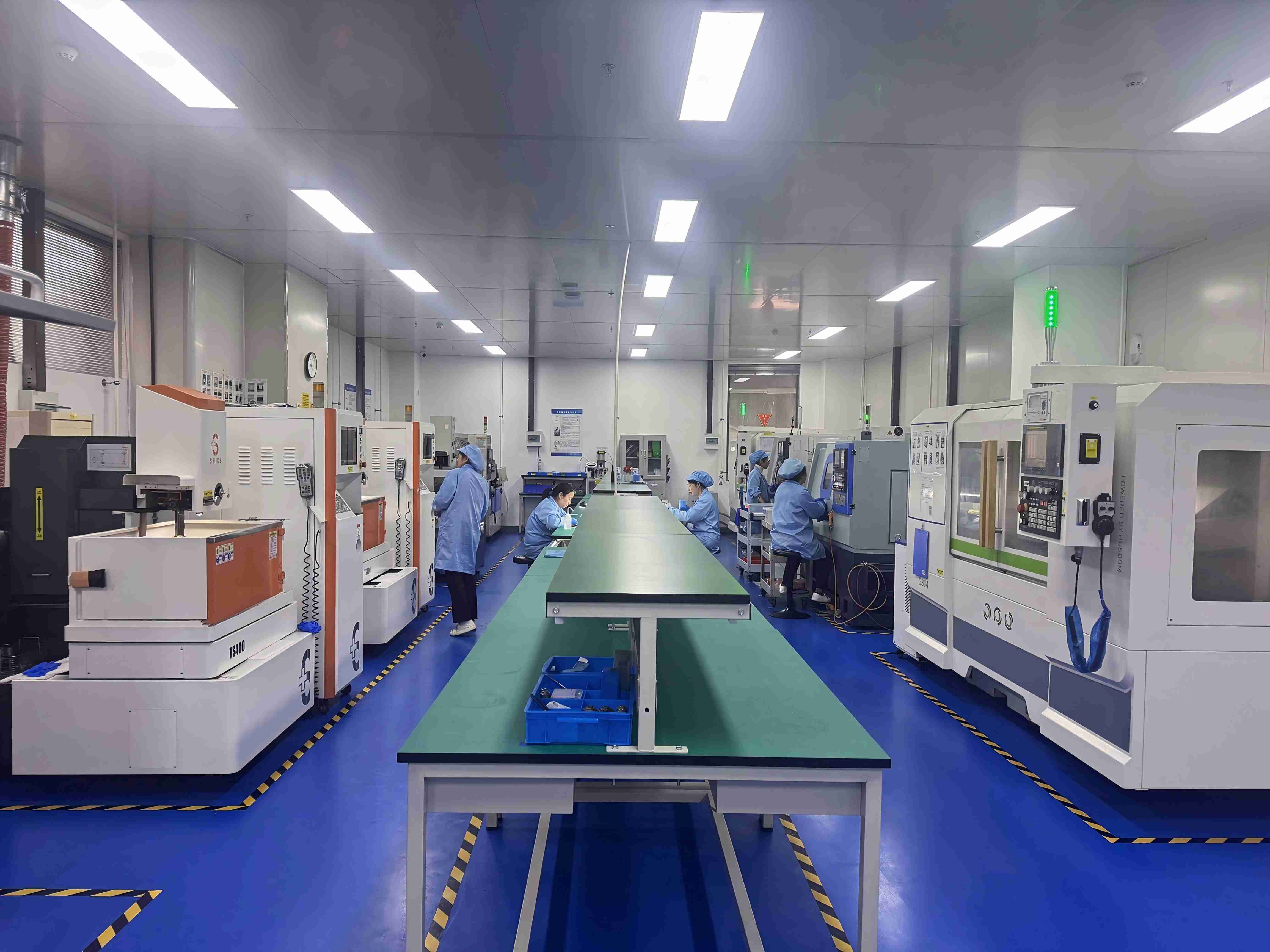
Optical device cutting areas are normally required to operate as Class 100/1000 cleanrooms, with constant temperature and humidity and anti-static conditions. Airborne particles settle on optical surfaces and inside cut channels; humidity swings change bond behaviour and can promote corrosion or static build-up; static discharge can damage sensitive device structures. These are not housekeeping details — they are part of the process specification that makes low-chipping performance repeatable.

Step-by-Step Breakdown: Qualifying a Low-Chipping Optical Cutting Process
A qualification sequence that treats blade, machine, environment and supply consistency as one program typically follows eight steps.
- Define the cut requirement. Record device material and stack, target kerf width, acceptable chipping limit, required cut depth and die dimensions. This becomes the acceptance reference for every later step.
- Short-list blade constructions. Match the workpiece to a construction family — a wafer sawing blade for silicon-based optical components, a functional ceramic blade for ceramic substrates, an alloy material blade for metal components, and an optical communication sawing blade where the device is intended for optical communication applications.
- Confirm machine and spindle condition. Measure spindle runout, verify flange condition and check coolant or air delivery before evaluating any blade. Machine condition determines whether a blade result is repeatable.
- Run a sample evaluation. Cut a representative batch and measure chipping, kerf width and cut position at the start, middle and end of the run — not only at the start. Most drift problems appear in the later part of a run.
- Set process parameters as a system. Fix spindle speed, feed rate, blade exposure and coolant flow together. Changing one parameter after qualification invalidates the edge-quality result.
- Verify environmental conditions. Confirm Class 100/1000 cleanroom status, temperature and humidity stability, and anti-static measures before production release, since these conditions are part of the process specification.
- Establish in-process monitoring. Define how often kerf width and edge quality are checked during a run and what triggers a blade change. Batch-level data tracking allows adjacent batches to be compared, which is how consistency is proved rather than assumed.
- Lock the supply arrangement. Agree MOQ, delivery terms, acceptance criteria and payment terms before volume ramp so that incoming blade lots carry the same specification that was qualified.
Use Cases: Optical Communication and Semiconductor Packaging Scenarios
Optical communication component singulation
Optical communication and optoelectronic devices combine brittle and semi-transparent materials with tight dimensional requirements. Chipping at a facet or a coupling surface affects optical performance, so blade selection prioritizes a bond that keeps cutting force low while maintaining edge definition, paired with a hubless or thin construction where the workpiece is thin. The 16% share of the dicing blade market held by optical communication and RF/optoelectronics applications reflects how much of this cutting is now production-scale rather than laboratory-scale.
Semiconductor packaging die separation
In packaging lines, die separation follows the same principles under higher volume pressure: stable kerf over long runs, controlled chipping to protect die strength, and blade supply that does not change specification between lots. This is where batch traceability and adjacent-batch comparison matter as much as blade grade, because a packaging line cannot absorb re-qualification every time a blade lot changes.
Functional ceramic substrates and precision alloy components
Ceramic substrates used in optical and electronic modules, and precision alloy components used in device housings and fixtures, require constructions suited to harder or more ductile materials. Metal bond blades are used where the material demands greater bond retention, while the same line may use electroforming hard or slotted constructions for specific geometries. A supplier with a full construction range lets buyers qualify one supplier relationship instead of several.
Comparison Tables
Table 1 — Blade constructions and their scenario fit
| Blade family | Construction focus | Typical evaluation scenario |
|---|---|---|
| DZY Series wafer sawing blade | Wafer-level dicing construction | Semiconductor wafer and optical device singulation |
| DZR Series sawing blade | Precision dicing construction | Optical communication components and general precision cutting |
| DZR-S Series slotted sawing blade | Slotted blade geometry | Cutting programs requiring a slotted blade format |
| Hubless sawing blade | No hub ring; reduced peripheral mass | Thin substrates and 300 mm processing where runout control matters |
| Electroforming hard sawing blade | Electroformed hard bond | Harder materials where bond retention drives blade life |
| Semiconductor wafer sawing blade | Wafer dicing construction | Semiconductor packaging and die separation |
| Optical communication sawing blade | Construction for optoelectronic devices | Optical communication component cutting |
| Functional ceramic sawing blade | Construction for brittle ceramic | Ceramic substrates and functional ceramic parts |
| Alloy material sawing blade | Construction for metallic workpieces | Precision alloy components and fixtures |
Table 2 — Verified market and standards reference for optical cutting
| Reference point | Published value | Source |
|---|---|---|
| Global wafer dicing blade market, 2024 | USD 1.19 billion | Market Research Intel |
| Alternative dicing blade market estimates, 2024 | USD 1.31 billion and USD 0.437 billion (scope differs) | Intel Market Research; Dicing Blade Market Insights |
| Optical communication and RF/optoelectronics share, 2024 | 16% (USD 69.9 million), driven by 5G infrastructure expansion | Intel Market Research |
| Bond type share, 2024 | Resin bond 42%; metal bond 33% | Dicing Blade Market Report 2026 |
| Hubless blade trend | Increasingly dominant for 300 mm wafer processing; reduced runout on substrates below 50 µm | Semiconductor Equipment Market Data |
| Tool categorization standard | ISO 22180:2019 — CVD diamond-coated vs. monocrystalline/polycrystalline diamond tools | ISO |
| Global diamond saw blade market | USD 8.60 billion in 2025, expected USD 10.16 billion by 2032 | Maximize Market Research |
| Named market participants in high-precision semiconductor dicing blades | DISCO Corporation, Tokyo Seimitsu (Accretech), Advanced Dicing Technologies (ADT), Asahi Diamond | Credence Research |
Table 3 — Order, acceptance and payment terms
| Item | Terms |
|---|---|
| MOQ — standard models | 100 pieces per order; negotiable for long-term cooperative customers or bulk purchase plans |
| MOQ — customized models | 500 pieces per order |
| Small-batch trial orders | Flexible MOQ adjustment below 500 pieces, with slight price adjustment based on customization complexity |
| Delivery terms | FOB / CIF |
| Acceptance criteria | Pre-shipment test; third-party inspection (SGS) |
| Payment terms | 30 / 70 |
Long-Term Supply: Capacity, Batch Consistency and Order Structure
For optical device cutting, the harder question is not which blade works in a sample but which supplier can deliver the same blade behaviour for years. Two supply-side factors matter most.
Capacity and continuity. WINTIME's production capacity covers more than 800,000 pieces per month for standard specifications and more than 80,000 pieces per month for customized and special-shaped products. That split matters for optical cutting programs, because a line usually runs a standard blade for volume production while periodically needing customized or special-shaped blades for new device variants.
Batch consistency. Batch-to-batch variation is a recognized risk in blade supply, and it affects stable mass production directly. The control approach combines standardized production process parameters and automated production equipment to reduce manual operation errors, a batch production data tracking system that records process parameters, and comparative testing of adjacent batches to confirm that performance has not shifted. On the management side, an ISO 9001 quality management system with standard operating procedures, dedicated quality inspectors tracking each production batch, and a batch quality file that allows any lot to be traced — and non-conforming batches to be recalled — is what turns consistency from a claim into a process. WINTIME operates on this basis, and its development work on ultra-thin wafer dicing blades has achieved thicknesses below 9 microns in process, a level reached in mass production by a limited number of manufacturers.
For buyers, the practical implication is that supply terms, technical support and traceability should be reviewed at the same time as blade specification. Long-term cooperative customers can negotiate MOQ structures that fit rolling production rather than one-off shipments, which is the difference between a blade purchase and a cutting program.
FAQ
What acceptance criteria and standards apply when ordering sawing blades for optical device cutting?
Orders are accepted against a pre-shipment test plus third-party inspection (SGS), with payment terms of 30/70 and delivery on FOB or CIF terms. On the standards side, diamond tools such as sawing blades fall under ISO 22180:2019, which distinguishes CVD diamond-coated from monocrystalline and polycrystalline types, and suppliers operating under an ISO 9001 quality management system maintain batch quality files that allow each production lot to be traced.
Can one blade supplier cover both optical communication components and semiconductor packaging cutting?
Yes, provided the supplier's range spans constructions rather than a single grade. WINTIME's range includes the DZY Series wafer sawing blade, DZR Series sawing blade, DZR-S Series slotted sawing blade, hubless, electroforming hard and diamond sawing blades, plus blades designated for semiconductor wafer, optical communication, functional ceramic and alloy material cutting. The company works with 35 engineers and has developed ultra-thin wafer dicing blades to below 9 microns in process.
What drives the cost of a low-chipping blade program?
Three cost drivers dominate. First, kerf width: a narrower kerf removes less material, which raises usable die area on expensive optical substrates. Second, blade consumption: bond hardness determines wear rate, so a blade that is too soft for the material increases replacement frequency. Third, order structure: standard models carry a 100-piece MOQ and customized models 500 pieces, while long-term cooperative customers or bulk purchase plans can negotiate MOQ, and small-batch trial orders below 500 pieces are supported with a slight price adjustment based on customization complexity.
How should a buyer validate a blade before mass production?
Validation should combine a small-batch trial order with measurement at the start, middle and end of the run, covering chipping, kerf width and cut position. Because batch-to-batch variation is a recognized risk, validation should also request adjacent-batch comparative testing and the batch production data record. Pre-shipment testing and optional SGS third-party inspection provide the documentation needed before a production release.
What supports lead time and long-term supply continuity?
Capacity and traceability. WINTIME runs more than 800,000 pieces per month for standard specifications and more than 80,000 pieces per month for customized and special-shaped products, with FOB/CIF delivery options and exports to Southeast Asia, East Asia, North America and Europe. Batch quality files allow any lot to be traced and non-conforming batches to be recalled. For buyers planning a long-term program, the fastest next step is to send the device material, target kerf and chipping limit for a sample and quotation discussion.
Conclusion
Low-chipping optical device cutting is not solved by blade grade alone. Narrow kerf, bond hardness, hubless stability, machine and spindle condition, dry or wet operation, and Class 100/1000 cleanroom conditions with stable temperature, humidity and anti-static control all have to be qualified as one system — and then held consistent across production batches. Suppliers that combine a full blade construction range with documented batch traceability, standardized process parameters and transparent order terms remove most of the variables that let chipping, kerf loss and dimensional drift reappear after a successful sample.
WINTIME Semiconductor Technology Co., Ltd. — No. 868, Fushou East Road, Rugao City, Jiangsu Province, China — produces high-precision wafer-level sawing blades and cutting solutions for optical communication, semiconductor packaging, functional ceramic and precision alloy cutting.
Next Step: Sample and Quotation
Send the device material, target kerf width and chipping limit to request a blade recommendation, a small-batch trial and a quotation. The full product catalogue and technical data are available in the downloadable brochure.
Download the WINTIME sawing blade brochure (PDF)
Email: shenxiangfei@ntwintime.com · Tel: +86 13851530812 · WhatsApp: +8618888053207
Website: en.wintime.net.cn
Have Questions or Need More Details?
Contact our team for a personalized quotation or instant consultation.
Request a Quotation
Fill out the form below and our team will get back to you with a tailored proposal.
WhatsApp Direct Chat
Prefer to chat in real-time? Message us on WhatsApp for instant assistance & quick answers.
- Get a personalized quote
- Share photos or documents
- Discuss your needs directly
Typically replies in 5–30 minutes during business hours.