
Nickel Blades vs. Resin Blades in Silicon Wafer Dicing: The Expert Break-Even Analysis
Answer first: resin-bond and nickel-bond (electroformed metal-bond) sawing blades do not fail in the same way, so they cannot be compared by price per piece. A resin bond gives up matrix material continuously, cuts silicon at lower force and generally keeps edge chipping low. A nickel electroformed bond holds diamond rigidly, keeps blade thickness and kerf width stable over a longer service interval, and can be produced at thicknesses a polymer matrix cannot hold. The break-even sits on four cost lines — blade consumption, kerf material loss, chipping-driven yield loss and blade-change downtime — and shifts with wafer format, street layout and the environmental class of the dicing area. WINTIME Semiconductor's ultra-thin wafer dicing blade programme has reached a blade thickness below 9 μm, which is the point at which this trade-off becomes measurable rather than theoretical.
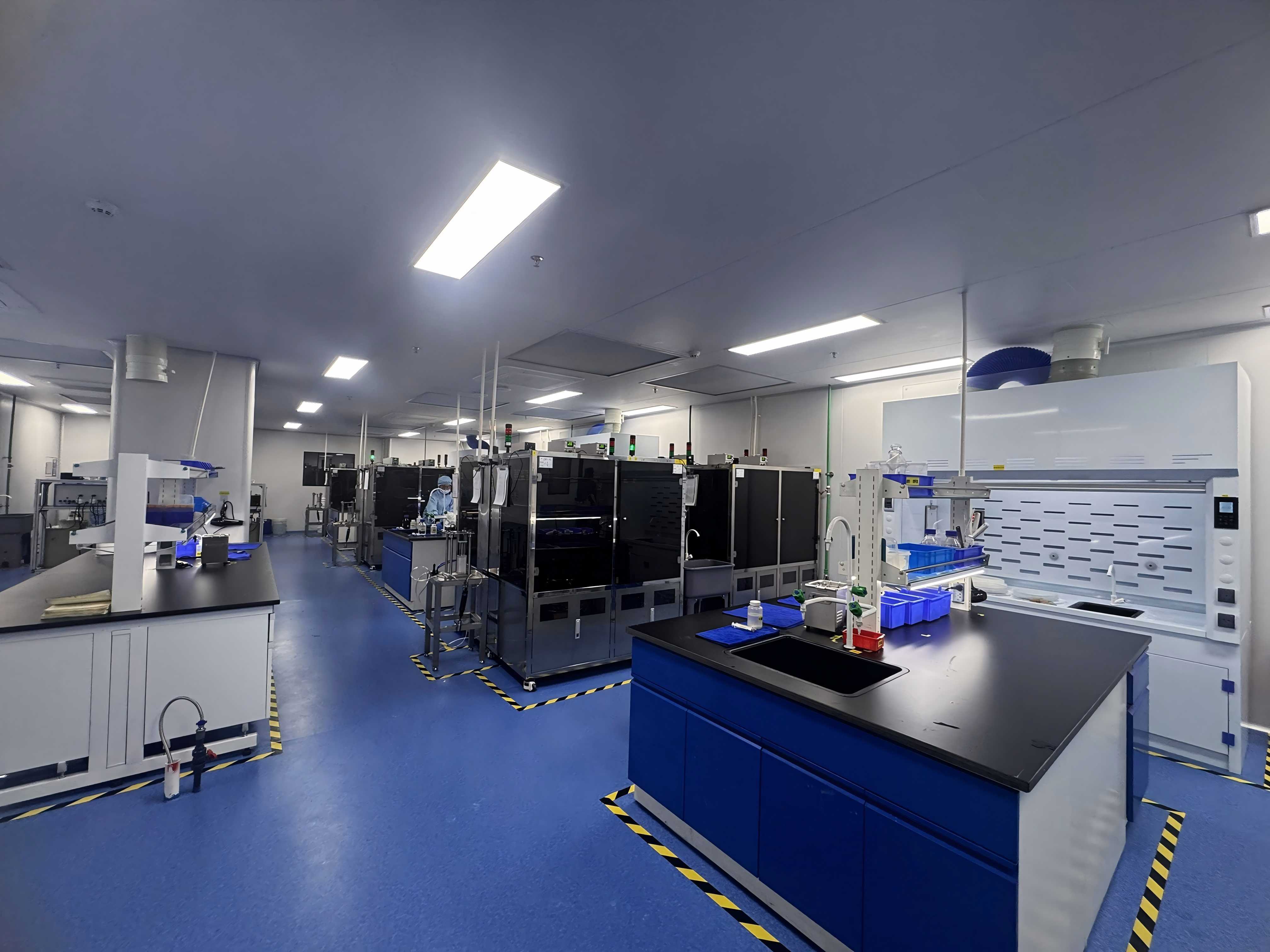
Nickel-bond and resin-bond sawing blades are finished and dimension-checked in the same production environment.
Problem Definition: Why the Bond Question Comes Back
Two sawing blades can carry identical drawings — same outer diameter, same spindle hole, same nominal thickness — and still deliver very different cost per good die. That gap is why the nickel-versus-resin question returns every time a line changes node, wafer thickness or street layout.
The failure modes are fundamentally different. A resin-bond blade is a composite: diamond abrasive held in a cured resin matrix that is deliberately softer than the workpiece. The matrix wears back during cutting and continuously exposes fresh diamond, so grinding force stays low and the silicon edge sees less mechanical damage. A nickel-bond blade is produced by electroforming, where nickel is grown around the diamond grit to form a dense, rigid metal matrix. Diamond retention is high, blade geometry is stiff and thickness is stable — but the bond does not give material back in the same way, so the cutting action is harder and the bond behaves differently at the die edge.
Procurement documents usually capture dimensions and sometimes grit size. They rarely capture the three values that actually decide the comparison: wafers per blade, kerf width at the end of blade life, and edge chipping at the specification limit. Without those three, a per-piece quotation cannot be converted into a cost per good die, and bond selection becomes a preference rather than an analysis.
Industry Background: What the Data Says About Bond Mix and Wafer Formats

Precision cutting blade manufacturing is concentrated in a small number of specialist plants.
The wider category gives context. The global diamond saw blade market was valued at approximately USD 8.60 billion in 2025 and is projected to reach USD 10.16 billion by 2032 (Maximize Market Research). The wafer dicing blade segment is far smaller but harder to size precisely: verified 2024 estimates range from roughly USD 0.44 billion to roughly USD 1.3 billion depending on whether the scope is drawn around blades alone or around equipment-adjacent consumables, with Intel Market Research and market.us behind that spread. For a buyer, the practical implication is simple — use market size for context, never as a proxy for what a specific blade will do on a specific line.
Bond mix is more directly useful. In 2024, resin-bond blades held 42% of the dicing blade market, while metal-bond blades — the family that includes nickel electroformed bonds and is used for harder materials such as SiC — accounted for 33% (market.us). Resin is therefore the majority convention in silicon dicing, not a compromise. Metal bond is the specialised minority that earns its place on harder substrates and on processes where geometry, rather than edge softness, is the constraint.
Wafer format drives the rest of the picture. Hubless dicing blades are increasingly dominant in 300 mm processing because they offer better stability and reduced runout on substrates thinner than 50 µm. Optical communication and RF/optoelectronics applications accounted for 16% of dicing blade market share in 2024, equivalent to USD 69.9 million, driven largely by 5G infrastructure expansion. Both trends push in the same direction — thinner substrates, narrower streets and tighter runout tolerances — which is exactly where nickel-bond geometry starts to compete with resin-bond edge quality.
One standards reference is worth anchoring before any specification discussion. ISO 22180:2019 covers diamond tools, including sawing blades, and distinguishes CVD diamond-coated types from monocrystalline and polycrystalline types. It is a classification standard rather than a performance guarantee, but it clarifies which product family a supplier is quoting. The competitive field around high-precision semiconductor dicing blades is documented as including DISCO Corporation, Tokyo Seimitsu (Accretech), Advanced Dicing Technologies (ADT) and Asahi Diamond, alongside specialist manufacturers such as WINTIME.
The Break-Even Model: Four Cost Lines, One Threshold

The comparison only becomes an analysis once blade price is converted into cost per good die.
The break-even is not a price comparison. It is the point at which the extra cost of a nickel-bond blade per unit of blade life equals the savings that blade produces in kerf and downtime. Written as a decision rule:
Nickel wins when: (blade price premium ÷ wafers per blade) < (kerf savings + downtime savings + kerf-drift scrap savings)
No supplier can fill those variables in for a buyer, because wafers per blade and chipping behaviour depend on the saw, the tape, the feed rate, the spindle and the device layout. What a supplier can do is supply both bond families with controlled geometry, so the buyer can run one test protocol across both.
Line 1 — Blade consumption
Blade price per piece is the most visible and the least decisive number in the comparison. Dividing it by wafers per blade converts it into a per-wafer cost. Nickel electroformed bonds hold diamond more rigidly and typically deliver a longer interval between blade changes; resin bonds wear back continuously, so they are usually replaced more often. On a high-volume line, the difference in change frequency is often what the process engineer notices first — not the invoice.
Line 2 — Kerf loss and kerf drift
Kerf is the material removed by the cut, and removed material is scrap. Total kerf loss per wafer scales with kerf width multiplied by total cut length, so small differences accumulate across thousands of streets. Nickel bonds hold thickness and kerf width more consistently across blade life, which matters when the specification is written at the last wafer rather than the first. Resin bonds, at very thin dimensions, can widen progressively as the matrix wears — the classic kerf drift pattern — so a blade may pass first-wafer inspection and fail at end of life.
Line 3 — Chipping and yield
Edge chipping is where resin bonds usually win on silicon. A softer, self-dressing matrix cuts at lower force, which generally produces less mechanical damage at the die edge — relevant for thin dice, narrow streets and devices with a low tolerance for micro-cracks. A rigid nickel bond transfers more force into the workpiece. On hard, brittle materials that rigidity is an advantage; on standard silicon it is a variable the buyer must measure rather than assume.
Line 4 — Environment, dressing and handling
Environmental class. In a controlled dicing environment, the controlling questions are particulate load and static behaviour. Resin-bond blades require periodic dressing to re-expose abrasive, which adds a process cycle and its own debris; because the matrix is polymeric, resin bonds do not provide the same conductive path as a metal bond, so static-control practice in the dicing area deserves attention. Nickel electroformed blades are monolithic metal, do not need a separate dressing cycle in the same way, and provide a conductive path.
Humidity and storage. Resin-bond blades are generally more sensitive to storage conditions, because a polymeric matrix can absorb ambient moisture; absorbed moisture can shift bond hardness and change break-in behaviour when the blade first enters the cut. Nickel electroformed blades, being dense metal, are not affected in the same way. For buyers in humid or coastal markets — including part of WINTIME's export base in Southeast Asia — the difference shows up in incoming inspection routines, packaging and shelf-life policy rather than in the cut itself. Both bond types should be stored and handled according to the supplier's specification.
| Cost line | What to measure | Why it moves between the two bonds |
|---|---|---|
| Blade consumption | Blade price; wafers per blade | Nickel bond retention typically extends blade life; a resin bond wears back faster |
| Kerf loss | Kerf width on first and last wafer; total cut length | Nickel holds kerf width across life; resin kerf can drift as the matrix wears |
| Yield loss | Edge chipping inspection; dies rejected at the spec limit | Resin cuts at lower force; nickel transfers more force into the workpiece |
| Downtime | Blade changes per shift; dressing cycles | Nickel reduces change frequency; resin adds dressing cycles |
| Environmental handling | Dicing area class; static controls; storage humidity | Resin adds dressing debris and no conductive path; nickel is monolithic metal |
| Commercial terms | MOQ, lead time, acceptance route, payment terms | Standard versus customized supply model changes the ramp cost |
Step-by-Step: Running the Break-Even Test on Your Own Line
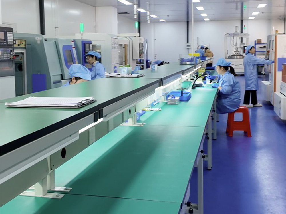
A structured trial is the only way to populate the break-even model with real line data.
- Convert the quotation into cost per good die. Take the per-piece price of each candidate blade and divide it by the wafers that blade actually completes before it is retired — not by a nominal figure from a datasheet.
- Track blade life in wafers per blade. Run both bond types over a fixed window on the same saw, tape and feed recipe, and log every blade change with a timestamp.
- Measure kerf width at both ends of blade life. Record kerf on the first wafer and on the last wafer of each blade. This single pair of numbers exposes kerf drift, which is where thin resin bonds most often lose the argument.
- Measure chipping at the acceptance limit. Inspect edge chipping at incoming die inspection for both bonds and count dies rejected at the specification limit, not the average.
- Add the environmental and handling lines. Include dressing consumables, the cleanroom class the process runs in, static-control measures, and any humidity-controlled storage required by the bond type.
- Run a sensitivity check. Repeat the arithmetic at two volumes and two wafer formats. The bond that wins at 300 mm high volume is not always the bond that wins on a low-volume, tight-edge-quality product line — so decide per product line, not per site.
Comparison Table: Nickel (Electroformed Metal Bond) vs. Resin Bond Sawing Blades
| Evaluation criterion | Nickel / electroformed metal bond | Resin bond |
|---|---|---|
| Bond matrix | Dense electroformed nickel grown around diamond grit | Cured resin matrix holding diamond abrasive |
| Diamond retention | High — rigid mechanical grip | Lower — bond wears back to release fresh grit |
| Self-dressing behaviour | Limited; no separate dressing board cycle in the same way | Continuous self-dressing during the cut |
| Cutting force on silicon | Higher force transferred to the workpiece | Lower force; generally gentler at the die edge |
| Chipping behaviour on silicon | Must be verified per device; rigidity is advantageous on hard, brittle materials | Typically lower chipping; suited to thin dice and narrow streets |
| Blade life / change frequency | Typically longer interval between changes | Typically shorter interval between changes |
| Kerf width stability | Holds thickness and kerf width across blade life | Kerf width can drift as the matrix wears at very thin gauges |
| Thickness capability | Supports ultra-thin geometry; WINTIME's programme has reached below 9 μm | Practical minimum is limited by matrix strength |
| Environmental class / static | Monolithic metal; provides a conductive path | Polymeric matrix; adds dressing debris, static control needs attention |
| Humidity and storage | Not moisture-sensitive in the same way | Generally more storage-sensitive; moisture can shift bond hardness |
| Typical process fit | Hard/brittle substrates including SiC; ultra-thin, narrow-kerf silicon work | Conventional silicon logic and memory at volume |
| 2024 share of the dicing blade market | 33% (metal bond, including use on harder materials such as SiC) | 42% |
Share data: market.us. Bond behaviour is described as typical performance and must be confirmed on the buyer's own tool, tape and device layout.
Use Cases: Where Each Bond Earns Its Place
Conventional-thickness silicon, high volume, tight chipping specification. Resin bond is normally the starting point. The process benefits from a self-dressing bond that keeps force low, and the blade-change interval is predictable. The analysis should still confirm kerf width at the end of blade life, because that is where a resin blade can drift out of tolerance in a narrow-street layout.
Ultra-thin wafers with a narrow kerf budget. As blade thickness falls, geometry becomes the binding constraint. WINTIME's ultra-thin wafer dicing blade project has achieved a thickness of less than 9 μm in process, a level the company describes as reached by a limited number of domestic manufacturers in mass production. At that scale, kerf consistency and blade stiffness matter more than unit blade price — which is where an electroformed nickel bond enters the comparison.
Hard and brittle substrates. Metal-bond blades are associated with harder materials such as SiC and held 33% of the 2024 dicing blade market partly on that basis. When one line mixes silicon and hard substrates, the bond decision should be made per material, not per machine.
300 mm wafers and substrates thinner than 50 µm. Hubless dicing blades have become increasingly dominant in 300 mm processing because of better stability and reduced runout on thinner substrates. Mounting format and bond type jointly determine runout behaviour, so the two should be evaluated as a pair rather than separately.
Optical communication and RF/optoelectronics. This application group accounted for 16% of the 2024 dicing blade market, USD 69.9 million, driven largely by 5G infrastructure expansion. Devices in this group tend to have small features and strict edge-quality requirements, which typically favours the gentler bond while kerf control remains a secondary constraint.
Functional ceramics and alloy components. These materials call for different grain size, concentration and bond hardness than silicon. The same break-even logic applies, but the chipping-versus-kerf weighting shifts with the material, which makes this a customisation decision rather than a catalogue decision.
OEM and Customization Fit: How WINTIME Handles Bond Selection

Dimension, hardness and dynamic balance checks support both bond families before shipment.
WINTIME Semiconductor Technology Co., Ltd. is a Chinese manufacturer founded in 2020 and based in Rugao City, Jiangsu Province, where it integrates the research, development, production and sales of high-precision wafer-level cutting blades. The company operates a 34,000 ㎡ plant with 100 employees, 35 engineers, an annual output of 1 million pieces of dicing blades and an export ratio of approximately 30%, with main markets in Southeast Asia, East Asia, North America and the European Union. Its product scope covers sawing blades and dicing blades, and its blade families include DZY series wafer sawing blades, DZR series sawing blades, DZR-S series slotted sawing blades, hubless and hub-type formats, and electroforming hard sawing blades, with application-specific options for semiconductor wafers, optical communication devices, functional ceramics and alloy materials.
For a nickel-versus-resin evaluation, the relevant capability is the ability to supply both bond families and to hold geometry across them. WINTIME provides OEM, ODM and customized production services, with customized specifications for different cutting materials and working conditions. The customization scope includes blade diameter, thickness and spindle hole size; bond type (metal bond, resin bond); diamond abrasive grain size and concentration; coating for anti-rust, heat dissipation or wear resistance; cutting performance targets such as cutting speed and service life; packaging, including special packaging for export; and special-shaped blades in non-standard sizes.
Production capacity for evaluation programmes is 800,000+ pieces per month for standard specifications and 80,000+ pieces per month for customized and special-shaped products. Quality control covers geometric dimension inspection with vernier calipers and laser diameter gauges, hardness and wear-resistance testing on a material testing machine, dynamic balance detection on a high-speed dynamic balance tester, and cutting performance simulation on the actual material. After-sales support includes cutting process matching and equipment adaptation, quality problem investigation and resolution within 48 hours, customized after-sales service for bulk procurement customers, long-term supply and inventory support, application training for new customers, and replacement or compensation for defective products caused by quality problems.
FAQ: Nickel vs. Resin Bond Sawing Blades
1. What standards and documentation should a nickel or resin bond sawing blade comply with?
ISO 22180:2019 is the reference standard for diamond tools, including sawing blades; it distinguishes CVD diamond-coated products from monocrystalline and polycrystalline types and classifies product families rather than guaranteeing cutting performance. At supply level, the documentation that matters is the quality record behind each batch: geometric dimension inspection with vernier calipers and laser diameter gauges, hardness and wear-resistance testing on a material testing machine, dynamic balance detection on a high-speed dynamic balance tester, and a cutting performance simulation test run on the customer's actual material. Pre-shipment testing combined with third-party inspection (SGS) is an available acceptance route for either bond type.
2. Can bond type, blade thickness and diamond specification be customized for a specific wafer process?
Yes. Bond type is a customization variable rather than a fixed catalogue attribute. WINTIME provides OEM, ODM and customized production services, including customized specifications for different cutting materials and working conditions. Customizable parameters include blade diameter, thickness and spindle hole size; bond type (metal bond or resin bond); diamond abrasive grain size and concentration; coating options for anti-rust, heat dissipation or wear resistance; cutting performance targets such as cutting speed and service life; packaging, including export packaging; and special-shaped or non-standard blade dimensions. The company's ultra-thin wafer dicing blade project has achieved a thickness of less than 9 μm in process.
3. Which cost items decide the budget, and when does a nickel blade pay back?
Blade budget is driven by bond type, thickness tolerance, diamond grain size and concentration, coating and packaging, not by a single list figure. Two commercial points are usually fixed early: minimum order quantity, which is 100 pieces per order for standard models and 500 pieces per order for customized models, with flexible MOQ adjustment and a slight price adjustment for small-batch trial orders below 500 pieces; and payment terms of 30/70 with FOB or CIF delivery. The payback question is separate. A nickel blade pays back when its price premium, divided by wafers per blade, is smaller than the kerf savings, downtime savings and kerf-drift scrap savings it generates. That calculation must be run with the buyer's own wafer value, machine hour rate and street layout.
4. How can both bond types be validated before committing to volume?
Run both bonds through one protocol. A trial order can be placed below the standard volume threshold: small-batch trial orders under 500 pieces are accepted with flexible MOQ adjustment and a slight price adjustment based on customization complexity. Standard products ship in 2–5 working days and customized products in 10–25 working days, adjustable for large orders. On the line, measure three values for each bond: wafers per blade, kerf width on the first and last wafer of blade life, and edge chipping at incoming die inspection. Acceptance can be structured around pre-shipment testing plus third-party inspection (SGS).
5. What are the delivery terms and after-sales support?
Standard specifications ship in 2–5 working days; customized orders take 10–25 working days, with the schedule adjustable for large orders. Monthly capacity is 800,000+ pieces for standard specifications and 80,000+ pieces for customized and special-shaped products, which supports both trial quantities and volume ramp-up. Delivery terms are FOB or CIF. Quality problems are investigated and resolved within 48 hours, and long-term supply guarantee with inventory support and product application training for new customers are available. To start a nickel-versus-resin comparison, request a sample set or a quotation through WINTIME's website at en.wintime.net.cn or by email at shenxiangfei@ntwintime.com.
Conclusion: Let the Cost Line Decide, Then Verify It
The choice between nickel and resin bond sawing blades in silicon wafer dicing resolves to one question: which cost line dominates the cost of a good die on this line? Where edge quality and low cutting force decide yield, resin bond remains the correct default, and it held 42% of the dicing blade market in 2024 for that reason. Where kerf width stability, blade life and blade-change frequency dominate — and especially where blade thickness has to go below the range a resin matrix can hold — an electroformed nickel bond moves the arithmetic in the other direction. Because WINTIME's ultra-thin wafer dicing blade programme has reached a thickness below 9 μm, that comparison can now be tested at the extremes instead of argued in the abstract.
Next Step
Request a sample set covering both bond types, a quotation, or the full product catalogue. Technical support for cutting process matching, equipment adaptation and acceptance criteria is available from the application team.
Website: https://en.wintime.net.cn
Email: shenxiangfei@ntwintime.com
Tel: +86 13851530812
WhatsApp: +8618888053207
Address: No. 868, Fushou East Road, Rugao City, Jiangsu Province

Sample sets, quotation and technical process matching are handled by the WINTIME application team.
Have Questions or Need More Details?
Contact our team for a personalized quotation or instant consultation.
Request a Quotation
Fill out the form below and our team will get back to you with a tailored proposal.
WhatsApp Direct Chat
Prefer to chat in real-time? Message us on WhatsApp for instant assistance & quick answers.
- Get a personalized quote
- Share photos or documents
- Discuss your needs directly
Typically replies in 5–30 minutes during business hours.