
Sawing Blade Application Guide for Optical Communication Device Cutting Projects
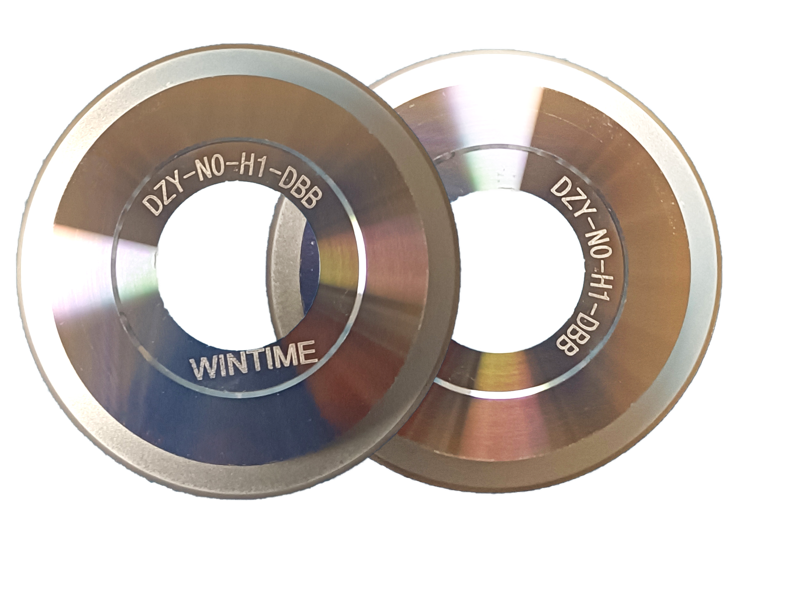
Short answer: An optical communication device cutting project needs a sawing blade that holds high-precision cutting, a narrow kerf, low chipping and stable dimensional control while the machine runs inside a Class 100/1000 cleanroom at 22±2°C and 45%–55% relative humidity, under dust-free and anti-static conditions. The cut itself is made by a high-speed spindle rotating at 30,000–60,000 rpm with precision feeding on an automatic dicing machine, and ultra-thin work can require a blade thickness of 9μm or less.
This guide is written for the people who have to fit a blade into that window: process engineers, equipment owners and buyers sourcing optical communication sawing blades. It maps the project conditions to blade construction, thickness, bond type and supporting equipment, then follows the sequence from specification review to final inspection and acceptance. Everything below is limited to documented blade capability and documented project conditions, so it can be used as a working reference rather than a marketing statement.
Problem Definition: Why Optical Communication Cutting Projects Reject Generic Blade Choices
Cutting an optical communication device is a scenario problem, not a blade-only problem. The blade has to satisfy three constraints at the same time: the geometry of the device, the cleanliness of the room, and the electrical safety of the die. A blade that cuts acceptably on a general wafer can still be the wrong choice here, because the limiting factor is usually not whether the blade cuts, but what it leaves behind — kerf width, edge condition, particles and drift.
The typical failure modes that project teams report in this scenario are:
- Kerf wider than the street. Excessive kerf consumes the dicing street and pushes die geometry outside tolerance, which reduces the usable area of every wafer in the batch.
- Chipping at the cut edge. Edge damage on brittle optical materials affects the mechanical strength of the die and its downstream optical performance.
- Dimensional drift during a run. If the blade wears unevenly, the cut position moves mid-batch, and package assembly starts to mismatch the incoming parts.
- Particle generation inside the cleanroom. Loose abrasive or bond debris in a Class 100/1000 environment is a yield problem, not a housekeeping problem.
- Static discharge risk. Anti-static control is a stated project requirement, because a static event near a finished die can damage the device.
- Blade wear before the batch ends. High wear resistance and long service life are listed project requirements precisely because blade changes interrupt continuous automatic operation.
In other words, the project does not buy a blade — it buys a stable cut inside a controlled environment. That is the standard against which every specification below should be read.
Industry Background: Where Optical Communication Cutting Sits in the Blade Market
Optical communication is no longer a niche corner of the dicing blade market. According to Intel Market Research, optical communication and RF/optoelectronics applications accounted for 16% of dicing blade market share in 2024, a value of approximately USD 69.9 million, driven by 5G infrastructure expansion. In the same year, Market Research Intel valued the global wafer dicing blade market at USD 1.19 billion, driven by semiconductor miniaturization and the adoption of 300mm wafers.
The broader diamond tool category is also expanding. Maximize Market Research valued the global diamond saw blade market at approximately USD 8.60 billion in 2025 and expects it to reach USD 10.16 billion by 2032. Inside that category, the mix of blade constructions matters for project planning: resin bond blades held a 42% share of the dicing blade market in 2024, while metal bond blades — used for harder materials such as SiC — accounted for 33%.
Two structural trends are relevant to optical communication cutting projects in particular. First, hubless dicing blades are increasingly dominant for 300mm wafer processing because of their superior stability and reduced runout on thinner substrates below 50µm. Second, supply is becoming more regional: China exports of cutting blades to Vietnam, India and South Korea grew between 2024 and 2025, with Vietnam increasing by USD 18 million and India by USD 12 million, according to the Observatory of Economic Complexity.
Standards matter as well. Diamond tools, including sawing blades, are categorized under ISO 22180:2019, which distinguishes between CVD diamond-coated and monocrystalline/polycrystalline types. That classification is the reference point when a project team needs to describe a blade in a specification document rather than by catalogue nickname.
Detailed Solution: How a Sawing Blade Adapts to an Optical Communication Cutting Project
WINTIME Semiconductor Technology Co., Ltd. is a Jiangsu-based manufacturer established in 2020 that integrates the research, development, production and sales of high-precision wafer-level cutting blades, cutting tapes and cutting solutions. The company operates a 34,000㎡ facility with 100 employees, including a 35-engineer R&D team, and reports an annual output of more than 1 million pieces of dicing blades with roughly 30% of production exported to Southeast Asia, East Asia, North America and the EU. Its completed ultra-thin wafer dicing blade project achieved a blade thickness of less than 9 microns in process, and the company states it is one of the few domestic producers able to mass-produce at that level.
Blade construction: what actually connects the spindle to the cut
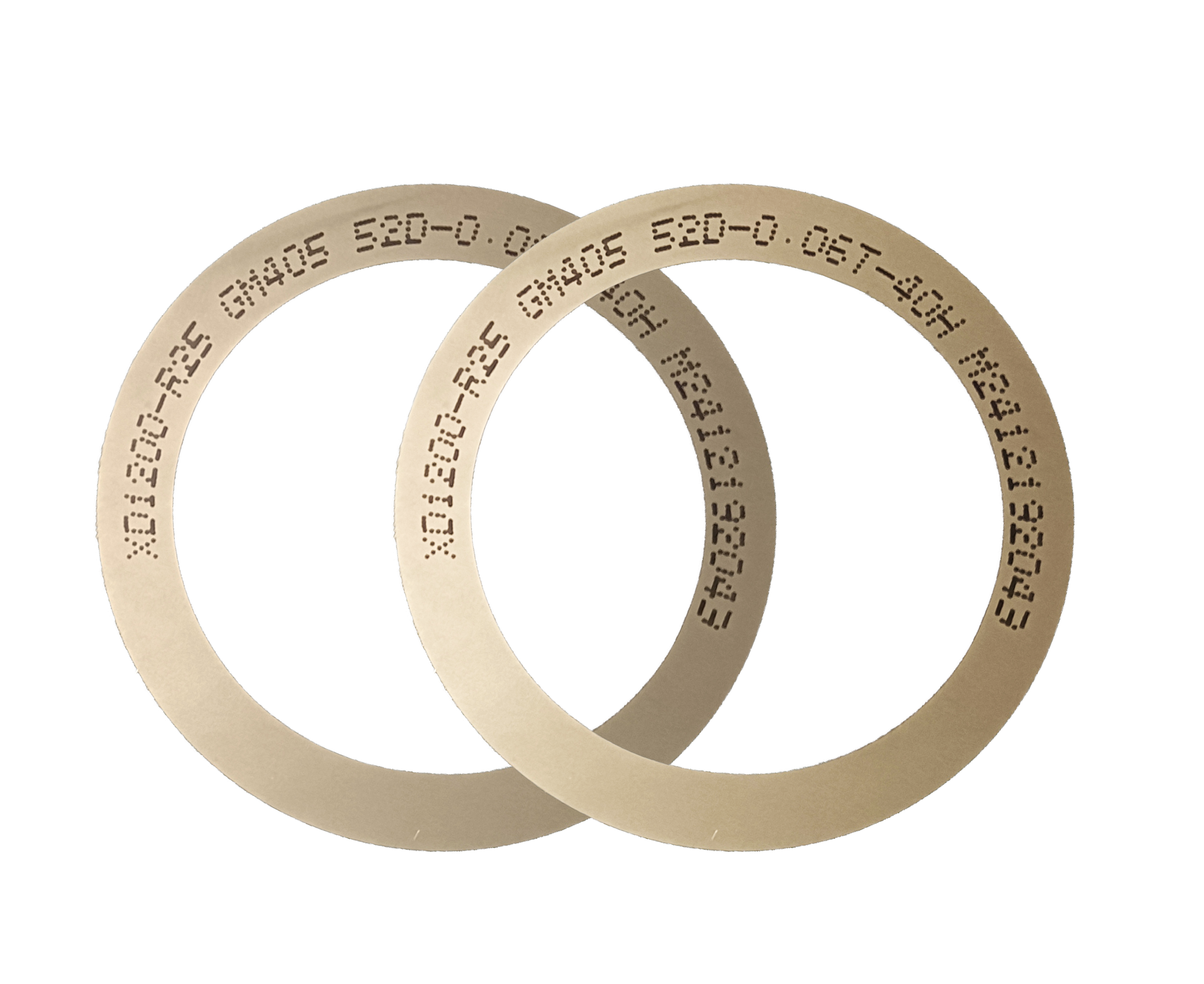
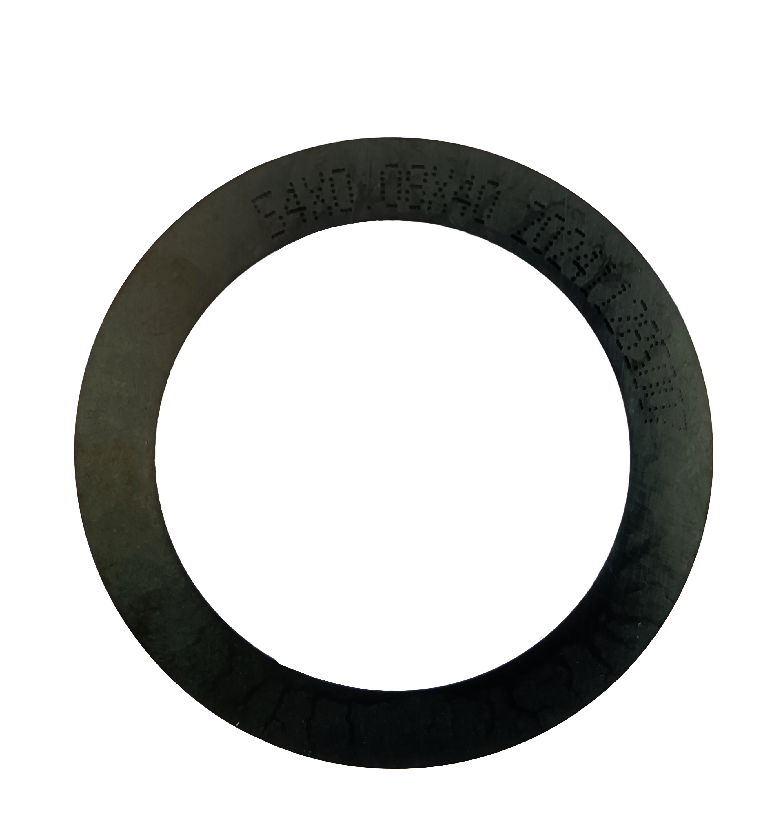
A sawing blade in this class is built from three functional parts: a diamond superabrasive as the cutting medium, a resin or metal bond matrix that holds the abrasive, and a high-strength steel base that carries the load. The bond matrix decides how the abrasive is retained and released, which in turn decides wear behaviour and edge quality. Because the blade type list for this product family spans diamond, precision, semiconductor, circular, hubbed, hubless and flanged sawing blades, plus the DZY Series wafer sawing blade, the DZR Series sawing blade and the DZR-S Series slotted sawing blade, a project team can match construction to the material stack instead of forcing one blade across every step.
Geometry options that answer the kerf problem
Kerf control comes from geometry before it comes from parameters. A hubless sawing blade is the usual direction when runout has to stay low on thin substrates, while slotted and flanged configurations are used where stability during high-speed rotation is the priority. For optical communication cutting, the practical question is whether the selected blade can hold a narrow kerf while the spindle runs between 30,000 and 60,000 rpm, and whether blade thickness can be pushed down for ultra-thin slicing without losing dimensional accuracy.
Parameter envelope for the project window
The documented specification envelope for this sawing blade is the baseline for any optical communication cutting project, because these are the values a process engineer has to match against the device map.
| Specification | Documented value |
|---|---|
| Blade thickness range | 8μm – 50μm |
| Cutting accuracy | ±0.002mm |
| Spindle speed | 30,000 – 60,000 rpm |
| Hardness | HRC 65 – 70 |
| Bond type | Resin / metal |
| Chip removal rate | ≥1.2mm³/s |
| Material | Diamond superabrasive, resin or metal bond matrix, high-strength steel base |
Keeping the blade inside the cleanroom envelope
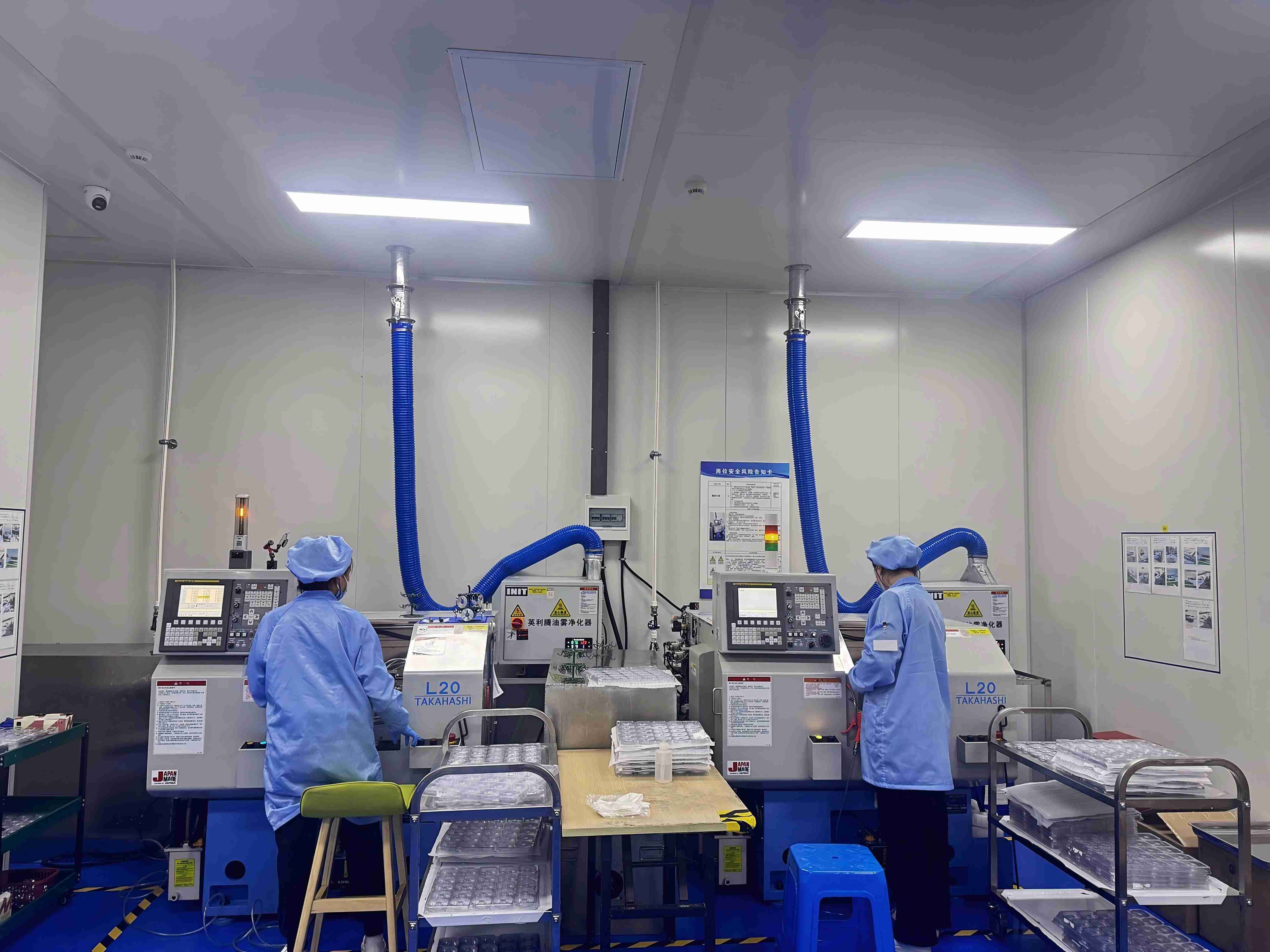
The project environment is as much a specification as the blade itself: Class 100/1000 cleanroom, constant temperature of 22±2°C, constant humidity of 45%–55%, dust-free and anti-static conditions, and a high-speed spindle environment with continuous automatic operation. These conditions shape the choice of coating and the acceptance criteria. Anti-static behaviour, low cutting loss and stable mass production are stated requirements rather than optional features, and they are the reason a blade that performs well in a general workshop is not automatically acceptable in this project.
Supporting equipment the blade must work with
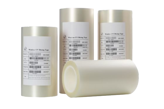
A blade never operates alone. The matched equipment set for this scenario includes the automatic wafer dicing machine, the semiconductor cutting spindle, the UV tape mounting machine, wafer cleaning equipment and the wafer testing machine. Cutting performance depends on how the blade behaves at the interface of all five: tape adhesion and flatness before the cut, spindle runout during the cut, cleaning effectiveness after the cut, and inspection data that confirms what the cut actually produced.
Step-by-Step: Setting Up a Sawing Blade Project from Specification to Acceptance
Step 1 — Translate the device map into cutting requirements
Start with the device, not the blade. Record the material stack, die thickness, street width and the minimum die strength the downstream process can accept. This step converts a device drawing into three numbers that drive everything else: target kerf, allowable chipping, and required dimensional tolerance. In an optical communication project, the tolerance usually has to sit inside the blade's documented ±0.002mm cutting accuracy.
Step 2 — Choose blade family and bond type
Select from the diamond sawing blade, semiconductor wafer sawing blade or DZY/DZR/DZR-S series families according to the material being cut, then choose resin or metal bond. Harder and more abrasive materials generally push the selection toward metal bond, while resin bond remains the most widely used construction in the global dicing blade market. Functional ceramic sawing blades and alloy material sawing blades are typically specified where the substrate is not silicon, and bonding and grain selection become more important than raw hardness alone.
Step 3 — Set the kerf budget through blade thickness
Blade thickness is chosen between 8μm and 50μm against the street width and the required die strength. Where the project involves ultra-thin wafer processing or optical device cutting with a tight geometry budget, the target can move toward a blade thickness of 9μm or less — the range covered by the company's ultra-thin dicing blade project.
Step 4 — Mount and align on the UV tape mounting machine
Tape mounting is where dimensional control begins. The UV tape mounting machine must deliver a flat, evenly tensioned wafer, because any local lifting shifts the cut line and shows up later as kerf drift. Because the requirement is dust-free operation, mounting should be treated as part of the cleanroom sequence, not as a pre-step outside it.
Step 5 — Configure the automatic dicing machine and spindle
Set spindle speed inside the 30,000–60,000 rpm range supported by the blade, confirm runout on the semiconductor cutting spindle, and programme precision feeding for continuous automatic operation. Hubless configurations are commonly preferred where runout control on thin substrates matters most. At this stage the process engineer also confirms that chip removal capacity — rated at ≥1.2mm³/s — is not the limiting factor for the chosen feed rate.
Step 6 — Decide dry cutting or wet cutting
Dry and wet cutting are both available on this equipment train, and the choice depends on how the material responds to heat and how much debris the room can tolerate. Wet cutting helps with cooling and particle transport; dry cutting simplifies the process where the material and the blade combination do not generate problematic heat. The decision should be recorded as part of the recipe, because switching mode after qualification invalidates the accepted parameters.
Step 7 — Monitor kerf, chipping and drift during the run
Sampling during the run is what separates a trial from a qualified process. Track kerf width, edge chipping and cut position across the batch. Because high wear resistance and long service life are stated project requirements, the useful monitoring output is not one good wafer, but a flat curve across many wafers.
Step 8 — Clean, inspect and lock the recipe
After dicing, wafers move to the wafer cleaning equipment and then to the wafer testing machine. Cleaning removes the debris that would otherwise become a contamination source in a Class 100/1000 room; testing confirms that dimensional control held. Lock the recipe with the inspection data attached, so that future blade lots can be compared against the same acceptance criteria.
Quality control steps behind the blade itself
The blade that arrives at the dicing machine has already passed four inspection stages: geometric dimension inspection with a vernier caliper and laser diameter gauge; hardness and wear resistance testing on a material testing machine; dynamic balance detection on a high-speed dynamic balance tester; and a cutting performance simulation test on the actual material. For optical communication projects, the simulation test is the most useful of the four because it exercises the material stack the project will actually run.
Use Cases: Where This Blade Configuration Fits
Optical device cutting and wafer dicing & scribing
This is the core project type. The blade is used for high-precision wafer cutting and scribing where narrow kerf and low chipping determine how much usable die comes out of each wafer. Stable dimensional control matters more here than maximum feed rate, because a shifted cut affects every downstream alignment.
Ultra-thin wafer processing
When the substrate is thin, runout and blade thickness dominate outcomes. Hubless sawing blades are increasingly used for 300mm wafer processing because of superior stability and reduced runout on substrates below 50µm, and a thickness of 9μm or less becomes the project target for the thinnest work.
Functional ceramic substrate cutting
Ceramic substrates behave differently from silicon: the material is harder and more brittle, so bond selection and grain characteristics do more work than blade geometry. Functional ceramic sawing blades are specified for these steps, with chip removal capacity and wear resistance as the practical constraints.
Precision alloy component cutting
Alloy material sawing blades are used where the cut has to meet the same dimensional accuracy but the workpiece is metallic rather than brittle. Here the limiting factor is usually blade life and heat, which is why wet or dry mode selection should be confirmed during qualification rather than assumed.
Semiconductor package cutting
On packaging lines, blades cut through molded and laminated structures where mixed materials can cause uneven loading. Stable mass production — not a single perfect cut — is the requirement, and the four-stage quality control sequence exists to support exactly that kind of repeated output.
Comparison Table: Project Requirements Against Blade Specification
The table below maps each documented project requirement to the blade property that answers it. Every entry is drawn from the documented project conditions and blade specification, not from estimated performance.
| Project requirement | How the sawing blade responds |
|---|---|
| Class 100/1000 cleanroom, dust-free operation | Blade used in a dust-free, anti-static environment with cleaning and inspection steps after cutting |
| Constant 22±2°C and 45%–55% humidity | Stable dimensional control is a stated blade function under these constant conditions |
| Anti-static requirement | Anti-static behaviour is a stated special requirement of the application |
| High-speed spindle rotating cutting | Blade rated for spindle speeds of 30,000–60,000 rpm |
| Automatic dicing machine with precision feeding | Continuous automatic operation and precision feeding cutting are supported operation modes |
| Narrow kerf | Blade thickness range of 8μm–50μm with cutting accuracy of ±0.002mm |
| Low chipping | Low chipping is a stated function of the blade in this scenario |
| Ultra-thin blade thickness ≤9μm | Ultra-thin wafer dicing blade project achieved less than 9 microns in process |
| High wear resistance and long service life | Hardness of HRC 65–70 and low cutting loss are documented properties |
| Stable mass production | Annual output of more than 1 million pieces of dicing blades |
The second table places the main construction options in their verified market context, which is useful when a project team has to justify a construction choice in a specification review.
| Construction option | Verified market context (2024–2025) | Project relevance |
|---|---|---|
| Resin bond blade | 42% share of the dicing blade market in 2024 | Widely used baseline construction; resin is one of the two documented bond types for this blade |
| Metal bond blade | 33% share of the dicing blade market in 2024; used for harder materials such as SiC | Metal is the second documented bond type and the usual direction for harder materials |
| Hubless blade | Increasingly dominant for 300mm wafer processing due to superior stability and reduced runout on substrates below 50µm | Relevant to ultra-thin slicing where runout control drives kerf and chipping |
FAQ: Optical Communication Sawing Blade Projects
What cleanroom and anti-static conditions must an optical communication sawing blade project meet, and which standard applies?
The documented project conditions are a Class 100/1000 cleanroom with constant temperature of 22±2°C, constant humidity of 45%–55%, dust-free and anti-static operation, and a high-speed spindle environment. Anti-static behaviour is listed as a special requirement of the application rather than an optional add-on. For terminology in specification documents, diamond tools including sawing blades are categorized under ISO 22180:2019, which distinguishes CVD diamond-coated from monocrystalline/polycrystalline types.
Can a sawing blade be customized for a kerf below 9μm and for different optical device materials?
Yes, within the documented customization scope. Blade diameter, thickness and spindle hole size; bond type including metal and resin; diamond abrasive grain size and concentration; coating for anti-rust, heat dissipation or wear resistance; cutting performance targets for speed and service life; export packaging; and special-shaped non-standard blade sizes can all be customized, with OEM and ODM production supported. On the ultra-thin side, the company's completed ultra-thin wafer dicing blade project achieved a thickness of less than 9 microns in process and the company states it is one of the few domestic producers able to mass-produce at that level.
What drives the cost of a sawing blade order for an optical communication cutting project?
Cost is driven by the specification, not by a single price point. The main drivers are blade diameter and thickness, bond type, diamond grain size and concentration, coating selection, whether a special-shaped non-standard blade is required, and order structure. Order minimums differ by type — 50 pieces for standard products and 300 pieces for customized products, with flexibility for long-term cooperative customers — and monthly capacity is above 800,000 pieces for standard specifications and above 80,000 pieces for customized and special-shaped products. A project that can consolidate its cutting steps into fewer standard specifications usually changes the cost profile more than negotiating on a single line item.
How is a sawing blade validated before a project scales into mass production?
Validation runs on documented test steps rather than on impressions. Each blade passes geometric dimension inspection with a vernier caliper and laser diameter gauge, hardness and wear resistance testing on a material testing machine, dynamic balance detection on a high-speed dynamic balance tester, and a cutting performance simulation test on the actual material. For a new optical communication project, that simulation test plus a pilot run at standard specification order quantities is the practical way to confirm kerf, chipping and dimensional control before committing to a production volume.
What are the lead times, order minimums and monthly capacity for these blades?
Standard products ship in 2–5 working days and customized orders in 10–25 working days, adjustable for large orders. Monthly capacity is more than 800,000 pieces for standard specifications and more than 80,000 pieces for customized and special-shaped products, and the company supports long-term supply guarantees and inventory support for bulk procurement customers, with quality problem investigation and resolution within 48 hours. To move from this guide to a project discussion, send the device map, street width and material stack to shenxiangfei@ntwintime.com or reach the team on WhatsApp at +86 18888053207, and request a matching sample or a project-specific quotation.
Conclusion: Fit the Blade to the Project Window, Not the Other Way Around
Optical communication device cutting projects succeed or fail on a narrow set of conditions: Class 100/1000 cleanliness, 22±2°C, 45%–55% humidity, anti-static operation, high-speed spindle cutting with precision feeding, and a blade that can hold a narrow kerf with low chipping and stable dimensional control. A blade with a thickness range of 8μm–50μm, cutting accuracy of ±0.002mm, HRC 65–70 hardness, resin or metal bond, and chip removal of ≥1.2mm³/s gives a project team a documented envelope to work inside, and the DZY, DZR and DZR-S series plus hubless configurations cover the geometry side of that problem.
The sequence matters as much as the specification: define the cutting requirement from the device, choose family and bond, set thickness against the kerf budget, control tape mounting, configure spindle and feed, decide dry or wet operation, monitor across the batch, then clean, inspect and lock the recipe. Projects that treat the blade as one element of that chain — rather than as a part number ordered at the end — are the ones that hold dimensional control through mass production.
WINTIME Semiconductor Technology Co., Ltd. supplies these sawing blades and cutting solutions from its 34,000㎡ facility in Rugao City, Jiangsu Province, with 35 engineers supporting cutting process matching and equipment adaptation for customers in China, Southeast Asia, East Asia, North America, the EU and other export markets.
Next step: sample and project quotation
Share your device map, street width, substrate material and target kerf, and the team will confirm the matching blade family, thickness and bond type. Standard specifications start at 50 pieces, customized blades at 300 pieces, and technical support for process matching is available before you place a production order.
Download the WINTIME product catalog (PDF)Request a sample on WhatsApp
Email: shenxiangfei@ntwintime.com · Tel: +86 13851530812 · WhatsApp: +86 18888053207 · Website: en.wintime.net.cn · Address: No. 868, Fushou East Road, Rugao City, Jiangsu Province, China
Have Questions or Need More Details?
Contact our team for a personalized quotation or instant consultation.
Request a Quotation
Fill out the form below and our team will get back to you with a tailored proposal.
WhatsApp Direct Chat
Prefer to chat in real-time? Message us on WhatsApp for instant assistance & quick answers.
- Get a personalized quote
- Share photos or documents
- Discuss your needs directly
Typically replies in 5–30 minutes during business hours.