
Sawing Blade Application Guide for Optical Device Cutting
Adapting a sawing blade to an optical communication device cutting project means fixing four measurable outputs before selecting a single blade parameter: kerf width, edge chip size, dimensional repeatability across the substrate, and cut-surface quality on the functional facet. Once those four targets are written down, bond type, diamond grain, blade thickness, spindle speed, feed rate, coolant strategy and cleanroom conditions become adjustable levers rather than trial-and-error guesses.
Optical communication devices are separated from brittle substrates at dimensions where the cut edge is not scrap — it is an optical surface. A waveguide end face, a fiber-array groove, or a lens rim that carries edge chipping will scatter light, shift insertion loss, or fail a downstream visual and optical inspection even when the die still meets its mechanical drawing. That changes the entire logic of blade selection.
This guide sets out how to adapt a sawing blade to an optical device dicing project end to end: the failure modes that matter, the market context, the blade configurations available from WINTIME Semiconductor Technology Co., Ltd., the cleanroom environmental window, dry and wet cutting on high-speed spindles, and the supporting equipment — automatic wafer dicing machines, semiconductor cutting spindles, UV tape mounting machines, wafer cleaning equipment and wafer testing machines — that ultimately decides whether a correctly specified blade performs on the line.
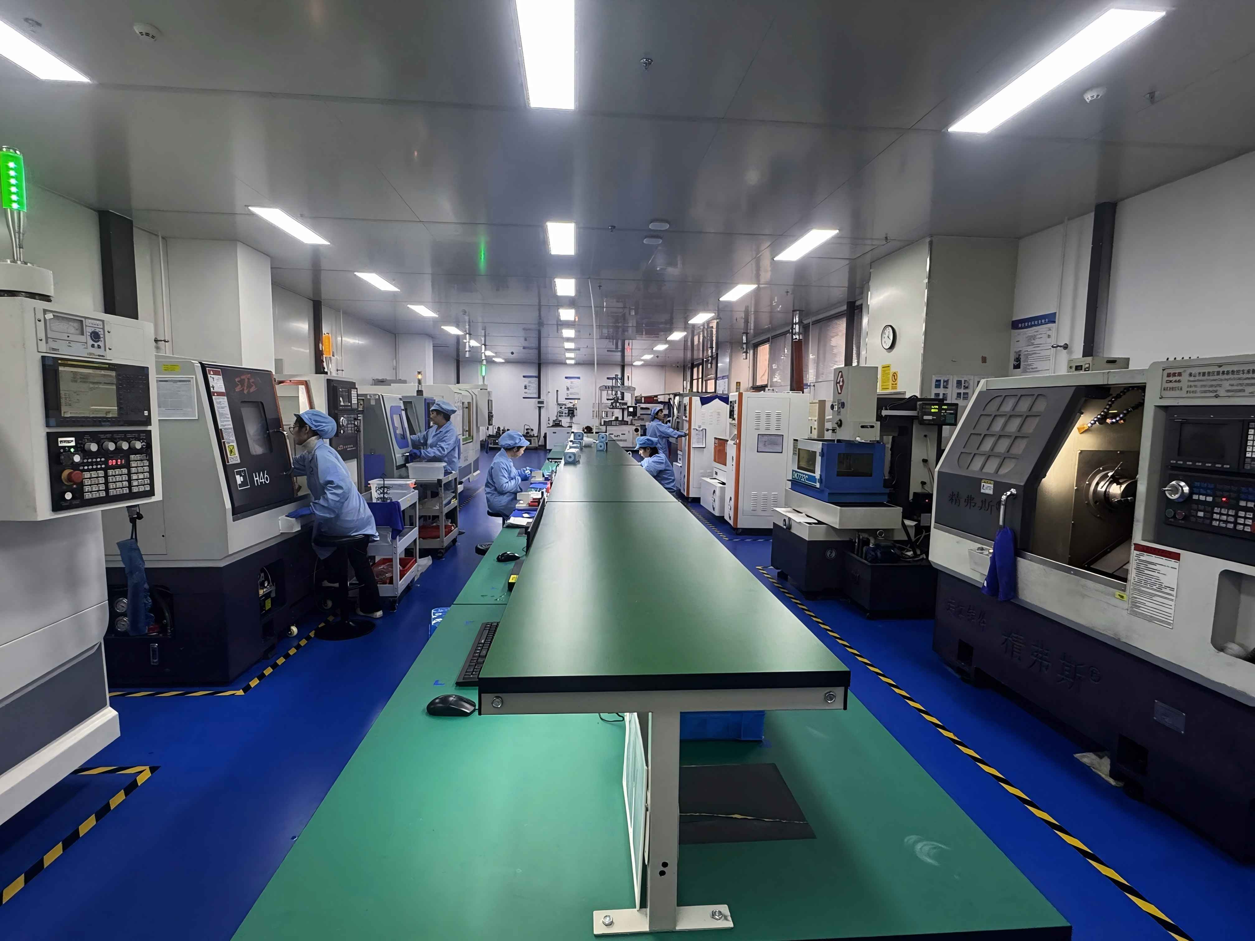
WINTIME Workshop — high-precision sawing blade manufacturing for wafer-level and optical device cutting projects.
Problem Definition: Why Optical Device Cutting Rejects Generic Blade Settings
An optical communication cutting project is defined less by the material it cuts than by what the cut edge has to do afterwards. Devices are singulated from substrates that are frequently transparent or semi-transparent, often built as multi-layer stacks, and almost always narrow in dicing street width. A blade that produces an acceptable edge on a logic die can still create an unacceptable optical surface, because the tolerance is measured in optical performance rather than in mechanical survival.
Four failure modes account for most yield loss in this application, and each one is governed by a different blade or process parameter:
- Edge chipping. Chip size at the cut edge is driven by bond hardness, diamond protrusion, feed rate and spindle speed. On an optical facet, chips of a size that would be cosmetic elsewhere can become a scattering site.
- Sub-surface micro-cracks. Brittle materials can carry damage below the kerf that is invisible at inspection and only propagates during later thermal cycling or cleaning. Ductile-mode or low-load cutting reduces this risk.
- Kerf and dimensional drift. Kerf width is the result of blade thickness, lateral vibration and wear over the run. Drift across a substrate shows up as out-of-tolerance die dimensions near the end of the cut.
- Particle and residue contamination. Abrasive debris, bond fragments and tape adhesive residue all land on surfaces that will later carry light. Cleanroom discipline and cleaning equipment are part of the blade specification, not an afterthought.
The economic logic follows from that list. A sawing blade is a consumable; an optical die is not. A blade decision that lowers the unit price of the consumable but raises edge chipping by even a small margin is a net loss. The correct evaluation basis is yield and repeatability across a lot — which is why a specification should be built from outputs backwards, not from a catalogue entry forwards.
Industry Background: Optical Communication's Place in the Dicing Blade Market
Optical communication is a meaningful and growing slice of dicing demand rather than a niche side line. According to Intel Market Research, optical communication and RF/optoelectronics applications accounted for 16% of the dicing blade market share in 2024, equivalent to roughly USD 69.9 million, with 5G infrastructure expansion cited as a principal driver. That figure sits inside a global wafer dicing blade market that Market Research Intel valued at USD 1.19 billion in 2024, supported by semiconductor miniaturisation and the shift toward 300 mm wafers.
Market sizing for this category should be read as directional rather than precise. Published estimates differ widely because the scope differs — some track consumable blades only, others include adjacent equipment and services. Reported figures for the same 2024 dicing blade metric range from roughly USD 0.437 billion to USD 1.31 billion depending on source and scope. For a procurement decision, the useful signal is not the headline number but the direction: demand is expanding, and optical applications are taking a larger share of it.
The wider diamond tooling context confirms the same trend. Maximize Market Research valued the global diamond saw blade market at approximately USD 8.60 billion in 2025, with an expected path to USD 10.16 billion by 2032. On the supply side, the Observatory of Economic Complexity records significant growth in China's exports of cutting blades to Vietnam, India and South Korea between 2024 and 2025, with Vietnam increasing by USD 18 million and India by USD 12 million — a signal that Asian blade supply is becoming more regionalised and more competitive.
Competitive structure in the high-precision segment is concentrated. Credence Research lists DISCO Corporation, Tokyo Seimitsu (Accretech), Advanced Dicing Technologies (ADT) and Asahi Diamond among the leading participants in high-precision semiconductor dicing blades. Alongside that, hubless dicing blades are increasingly dominant for 300 mm wafer processing, because they offer superior stability and reduced runout on thinner substrates below 50 µm — a construction trend that matters directly for optical device work, where thin and low-stiffness substrates are common.
The Solution: Configuring a Sawing Blade Around the Device, the Machine and the Room
WINTIME Semiconductor Technology Co., Ltd. is a Jiangsu-based manufacturer of high-precision wafer-level cutting blades and cutting solutions, established in 2020, operating a 34,000 m² facility with 100 employees, a 35-engineer R&D team and an annual output capacity of more than 1 million dicing blades. Around 30% of output is exported, with main markets in Southeast Asia, East Asia, North America and the EU. The company provides OEM, ODM and customized production services, including specifications tailored to different cutting materials and working conditions.
For an optical communication cutting project, that customization scope is the relevant capability — not a single fixed blade model. The configuration decisions below are the ones that actually move the four output targets.
Bond and abrasive: the first specification decision
Bond type sets the mechanical character of the cut. According to market analysis by market.us, resin bond blades held a 42% share of the dicing blade market in 2024, while metal bond blades — used for harder materials such as SiC — accounted for 33%. Resin bond blades are generally associated with good self-sharpening behaviour and lower mechanical stress at the cutting edge, which suits chipping-sensitive work. Metal bond blades generally offer stronger grit retention and longer life, at the cost of higher cutting loads and a greater need for controlled cooling and dressing.
For optical communication devices, the starting point is usually dictated by how much edge damage the functional facet can tolerate. Where the cut edge carries light, prioritising edge quality over blade life is normally the correct trade. Diamond grain size and concentration then refine that choice: finer grain generally improves edge finish while raising cutting load and reducing removal rate, and concentration affects how that load is distributed across the working surface.
Hubless construction for thin substrates and high spindle speeds
Hubless construction removes the hub and its mass from the rotating assembly, which reduces runout and improves stability on thin substrates. That is the mechanism behind the technology trend noted earlier: hubless dicing blades are increasingly dominant for 300 mm wafer processing and for substrates below 50 µm. Optical device substrates frequently fall into exactly that low-stiffness range, where a hub introduces both inertia and a lever arm that amplify any spindle error.
WINTIME supplies both hubless and hub-type configurations across its blade series, including the DZY Series wafer sawing blade, the DZR Series sawing blade, the DZR-S Series slotted sawing blade, and electroforming hard sawing blades. The series name identifies the configuration family; the actual specification — diameter, thickness, spindle hole, bond, grain and concentration — is set per project.
Narrow kerf and stable dimensional control
Kerf width is the sum of blade thickness, lateral vibration and wear. Narrowing it increases die-per-substrate yield, but it also reduces lateral stiffness, which makes the blade more sensitive to spindle runout, flange condition and feed strategy. Narrow kerf is therefore a system property rather than a blade-only property.
WINTIME's completed Ultra-thin Wafer Dicing Blade project achieved a thickness below 9 microns in the process, with product quality reaching the international cutting-edge level, and the company is one of the few domestic manufacturers able to achieve mass production of this specification. In practical terms, ultra-thin capability is what allows an optical project to reduce kerf without simply accepting a shorter blade life — provided the machine, the spindle and the tape support it.
Cleanroom and environmental control
Optical device dicing is normally performed in a controlled environment in the Class 100 to Class 1000 range, with air temperature held at 22 ± 2 °C and relative humidity at 45%–55%. Each of those three parameters maps onto a physical mechanism:
- Temperature. Spindle thermal growth changes blade exposure and depth of cut over a shift. Substrate and blade also expand and contract, so a room that drifts outside the window produces dimensional drift that looks like blade wear.
- Humidity. Low humidity raises static risk during UV tape handling and dry cutting; high humidity affects resin bond behaviour and can promote residue on optical surfaces.
- Particle class. Bond fragments and kerf debris must be captured by extraction, coolant flow and filtration rather than allowed to settle on functional surfaces.
For a project that spans multiple machines, the environment should be specified once and monitored continuously, because two dicing rooms with different stability will produce two different yields from the same blade batch.
Dry cutting versus wet cutting on high-speed spindles
Wet cutting supplies coolant directly to the cut zone, which removes heat, flushes debris and reduces thermal stress on brittle material. Its cost is downstream: liquid and debris must be removed completely, which places the cleaning step on the critical path. Dry cutting removes the liquid residue problem and simplifies cleaning, but it concentrates heat at the edge and makes debris evacuation harder.
Because optical surfaces are residue-sensitive, the choice is rarely made on cutting speed alone. A wet process with a validated cleaning and drying route is often the more controllable option, while a dry process is selected where liquid contact is unacceptable and the thermal budget can be shown to be safe. On the spindle side, higher rotational speed reduces chip load per grit and generally improves edge quality, but it also amplifies the effect of any radial or axial runout — which is precisely why hubless construction and spindle condition are treated together in this application.
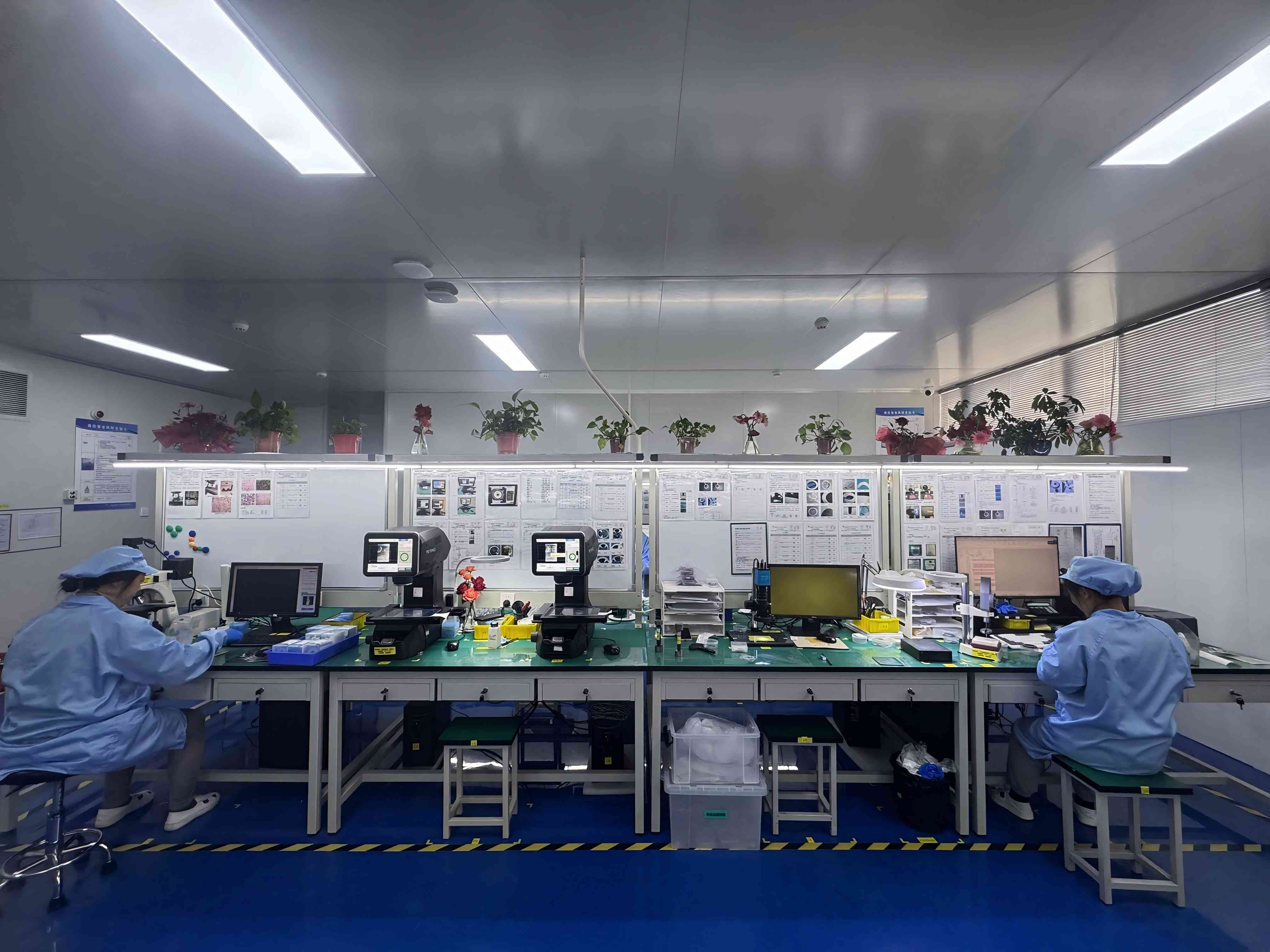
Geometry and balance verification before release — the step that keeps narrow-kerf optical cuts repeatable.
Supporting equipment that decides whether the blade performs
A blade reaches its specification only inside a matched equipment chain. In an optical communication cutting line, five items determine the outcome:
- Automatic wafer dicing machine. Sets alignment, index accuracy, feed resolution and blade exposure. Index error appears directly as dimensional scatter across the substrate.
- Semiconductor cutting spindle. Determines the usable speed range along with radial and axial runout. A narrow-kerf blade cannot compensate for a spindle that is already at its runout limit.
- UV tape mounting machine. Controls tape tension, flatness and bubble-free mounting. Poor mounting reduces support stiffness under the cut and allows die displacement.
- Wafer cleaning equipment. Removes kerf debris and adhesive residue without damaging the fragile cut edge — the step that determines whether a wet process is actually cleaner than a dry one.
- Wafer testing machine. Provides pre-cut and post-cut measurement, closing the feedback loop between blade specification and optical or electrical result.
Step-by-Step: Adapting a Sawing Blade to an Optical Cutting Project
Step 1 — Characterise the device stack and the cut
Record substrate material, total thickness, layer structure, dicing street width, and the distance from the street to the nearest functional feature. Note whether metal, dielectric or coating layers are present, because they change chip formation and coolant compatibility. This step produces the constraint set that every later decision must satisfy.
Step 2 — Write the four output targets
Define kerf width, maximum acceptable edge chip size, dimensional repeatability across the substrate, and the inspection method for facet quality. Agree these with the blade supplier before sampling, because a target that is only described qualitatively cannot be verified later.
Step 3 — Select bond and diamond specification
Choose resin or metal bond according to edge tolerance and material hardness, then set diamond grain size and concentration against the required edge finish and removal rate. WINTIME's customization scope covers bond type (metal bond, resin bond) and diamond abrasive grain size and concentration, so this step is a specification exercise rather than a catalogue lookup.
Step 4 — Match blade geometry to the spindle and the machine
Fix blade diameter, thickness and spindle hole size, confirm flange condition and exposure setting, and verify that the machine's speed and runout capability support the intended kerf. Blade diameter, thickness and spindle hole size, plus special-shaped blade customization for non-standard dimensions, are all within the customizable scope.
Step 5 — Lock the environment
Set and monitor the cleanroom class, temperature window and humidity window. Treat deviation as a process event that requires investigation, because environmental drift and blade wear produce very similar dimensional symptoms.
Step 6 — Decide dry or wet, then define the cleaning route
Select the cutting mode against the thermal budget and the residue tolerance of the optical surface, then specify coolant type, flow and nozzle position, followed by the cleaning and drying sequence. Coating options such as anti-rust, heat-dissipation and wear-resistant coatings can be specified where the process benefits from them.
Step 7 — Validate through sampling, inspection and release
WINTIME's quality control sequence covers four checks: geometric dimension inspection using vernier caliper and laser diameter gauge; hardness and wear resistance testing on a material testing machine; dynamic balance detection on a high-speed dynamic balance tester; and cutting performance simulation testing on actual material. A project then moves through sample cutting on the customer's own machine, pilot lot verification against the four output targets, and production release.
Timing note for project planning. WINTIME quotes 2–5 working days for standard products and 10–25 working days for customized orders, with adjustment possible for large orders. Building the sampling and pilot phase into the project schedule from the start avoids compressing validation into the production ramp.
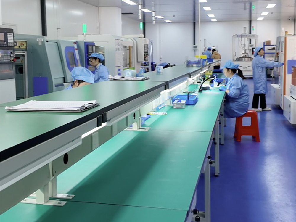
Customized orders are produced to the specification agreed at sampling — diameter, thickness, bond, grain and coating.
Use Cases: Where the Configuration Changes
Planar lightwave circuit and waveguide chip singulation
Waveguide chips require a clean end face because the cut itself creates the optical interface. Edge chipping and sub-surface damage matter more than removal rate, which pushes the specification toward finer diamond grain, lower feed per pass, and a bond that keeps cutting stress low. Narrow kerf is valuable here because street width is limited, but it must be supported by a spindle with margin on runout.
Fiber array and V-groove substrate dicing
Fiber array substrates combine tight groove pitch with brittle material, so dimensional repeatability across the substrate is the dominant output. Kerf drift late in the run shows up as pitch error, which makes blade wear monitoring and dynamic balance more important than raw cutting speed. Tape flatness from the UV tape mounting machine directly affects groove position accuracy in this case.
Ceramic ferrules, sleeves and functional ceramic parts
Ceramic components used in optical connectors are hard and wear the blade quickly, so blade life and kerf stability compete with edge quality. Metal bond configurations are generally favoured where hardness dominates, while functional ceramic sawing blades are specified to hold dimension over longer runs. Coolant delivery and debris evacuation decide whether the blade reaches its rated life.
LiNbO3 modulators and precision alloy components
Optoelectronic modulator substrates and precision alloy housings present two different problems in the same project: a brittle, damage-sensitive material and a ductile or mixed material that behaves very differently under the same blade. Alloy material sawing blades and optical communication sawing blades are therefore specified separately within one line, rather than standardised on a single part number.
Specification Reference: What Can Be Customized and Why It Matters
The table below summarises the customization levers available for an optical communication cutting project and the process outcome each one controls. It reflects WINTIME's stated customization scope; the specific value for any lever is set per project.
| Customization lever | What can be specified | Process outcome it controls |
|---|---|---|
| Blade geometry | Blade diameter, thickness and spindle hole size | Kerf width, die-per-substrate yield, machine fit and exposure setting |
| Bond type | Metal bond or resin bond | Edge chip level versus grit retention and blade life |
| Abrasive specification | Diamond abrasive grain size and concentration | Cut-surface finish, cutting load and removal rate |
| Coating | Anti-rust, heat-dissipation, wear-resistant coatings | Thermal behaviour at the cut zone, corrosion resistance and service life |
| Cutting performance | Cutting speed and service life targets | Cycle time balance against dimensional stability across the run |
| Packaging | Standard packaging and special packaging for export | Blade protection in transit and cleanroom-compatible handling on arrival |
| Special shapes | Special-shaped blade customization for non-standard dimensions | Fit to non-standard spindles, fixtures or cut geometries |
Two configuration families sit across those levers. Resin bond blades represented 42% of the dicing blade market in 2024 and metal bond blades 33%, according to market.us — a split that reflects the trade-off between edge quality and hardness capability rather than a ranking of quality. Hubless construction addresses a separate problem entirely: stability and runout on thin substrates, where the technology is increasingly dominant for 300 mm processing and substrates below 50 µm.
Frequently Asked Questions
Which standards and acceptance checks apply to a sawing blade for optical device cutting?
Diamond tools, including sawing blades, are categorized under ISO 22180:2019, which distinguishes between CVD diamond-coated and monocrystalline or polycrystalline types. On the commercial side, WINTIME's acceptance criteria are pre-shipment testing plus third-party inspection by SGS, with delivery terms available as FOB or CIF and payment terms of 30/70. Internal quality control covers geometric dimension inspection, hardness and wear resistance testing, dynamic balance detection and cutting performance simulation on actual material, so a buyer can align incoming inspection with the same four checks.
Can a sawing blade be customized for a specific optical material and dicing machine?
Yes. WINTIME provides OEM, ODM and customized production services, including customized specifications for different cutting materials and working conditions. The customizable scope covers blade diameter, thickness and spindle hole size; bond type (metal bond or resin bond); diamond abrasive grain size and concentration; coating options for anti-rust, heat-dissipation and wear resistance; cutting performance targets for speed and service life; packaging including special export packaging; and special-shaped blades for non-standard dimensions. This is what allows a single supplier to cover both a brittle optical substrate and a precision alloy component within the same production line.
What drives the cost of a customized optical communication sawing blade?
Cost is driven by customization complexity and order volume rather than by blade size alone. Minimum order quantities differ between standard models and customized models, and small-batch trial orders can be handled with a flexible MOQ adjustment and a slight price adjustment that reflects customization complexity. MOQ is also negotiable for long-term cooperative customers or bulk purchase plans. Because bond, grain, coating and special-shape requirements all change the production route, the practical approach is to fix the four output targets first and then price the configuration that meets them.
How are samples validated before a full production run?
Sampling starts with the material and machine data from the project, followed by cutting performance simulation on actual material as part of WINTIME's quality control sequence. The sample is then run on the customer's own dicing machine so that spindle behaviour, tape mounting and cleanroom conditions are included in the result. Validation is judged against the four agreed outputs — kerf width, edge chip size, dimensional repeatability and facet quality. Standard products are quoted at 2–5 working days, while customized and special-shaped items require 10–25 working days, so sample lead time should be planned into the project schedule.
What lead times and supply guarantees apply to volume orders?
Standard products are quoted at 2–5 working days and customized orders at 10–25 working days, adjustable for large orders. WINTIME's after-sales commitments include technical support for cutting process matching and equipment adaptation, quality problem investigation and resolution within 48 hours, customized after-sales service for bulk procurement customers, long-term supply guarantee with inventory support, product application training for new customers, and replacement or compensation for defective products caused by quality problems. The full specification scope and commercial terms are set out in the WINTIME product brochure, and project-specific questions can be sent directly to the contact details below.
Conclusion: Fix the Outputs, Then Fix the Blade
Optical communication device cutting rewards a project team that specifies backwards. The material stack and the functional facet set the four outputs; the outputs set the bond, grain, geometry and coating; the geometry sets the spindle and machine requirement; and the cutting mode sets the cleanroom and cleaning route. When that chain is built in order, a narrow-kerf blade with low chipping and stable dimensional control is an outcome rather than a hope.
The equipment around the blade deserves equal attention. An automatic wafer dicing machine, a semiconductor cutting spindle in good condition, a UV tape mounting machine that delivers flat, bubble-free mounting, wafer cleaning equipment that removes residue without touching the edge, and a wafer testing machine that closes the feedback loop are what convert a blade specification into consistent yield. In a Class 100 to Class 1000 room held at 22 ± 2 °C and 45%–55% relative humidity, those elements behave predictably — and predictability is the actual product being purchased.
WINTIME Semiconductor Technology Co., Ltd. supports that process with OEM, ODM and customized production, a 35-engineer R&D team, an annual output capacity of more than 1 million dicing blades, and process-matching technical support on the customer's own equipment. For projects moving from evaluation into execution, the fastest route is to send the device stack, street width and machine data, and let the blade specification follow from the four outputs.
Next Step: Sample, Quote or Technical Review
Send your substrate material, thickness, dicing street width, target kerf and machine model to receive a matched blade specification, a sample plan and a quotation for your optical communication cutting project.
Email: shenxiangfei@ntwintime.com | Tel: +86 13851530812 | WhatsApp: +8618888053207
Address: No. 868, Fushou East Road, Rugao City, Jiangsu Province | Website: en.wintime.net.cn
Sample requests, specification reviews and quotations are handled through the WINTIME project team.
Have Questions or Need More Details?
Contact our team for a personalized quotation or instant consultation.
Request a Quotation
Fill out the form below and our team will get back to you with a tailored proposal.
WhatsApp Direct Chat
Prefer to chat in real-time? Message us on WhatsApp for instant assistance & quick answers.
- Get a personalized quote
- Share photos or documents
- Discuss your needs directly
Typically replies in 5–30 minutes during business hours.