
Sawing Blade Best Practices in the Optical Communications Industry: Cleanroom, ESD and Straight-Cut Control
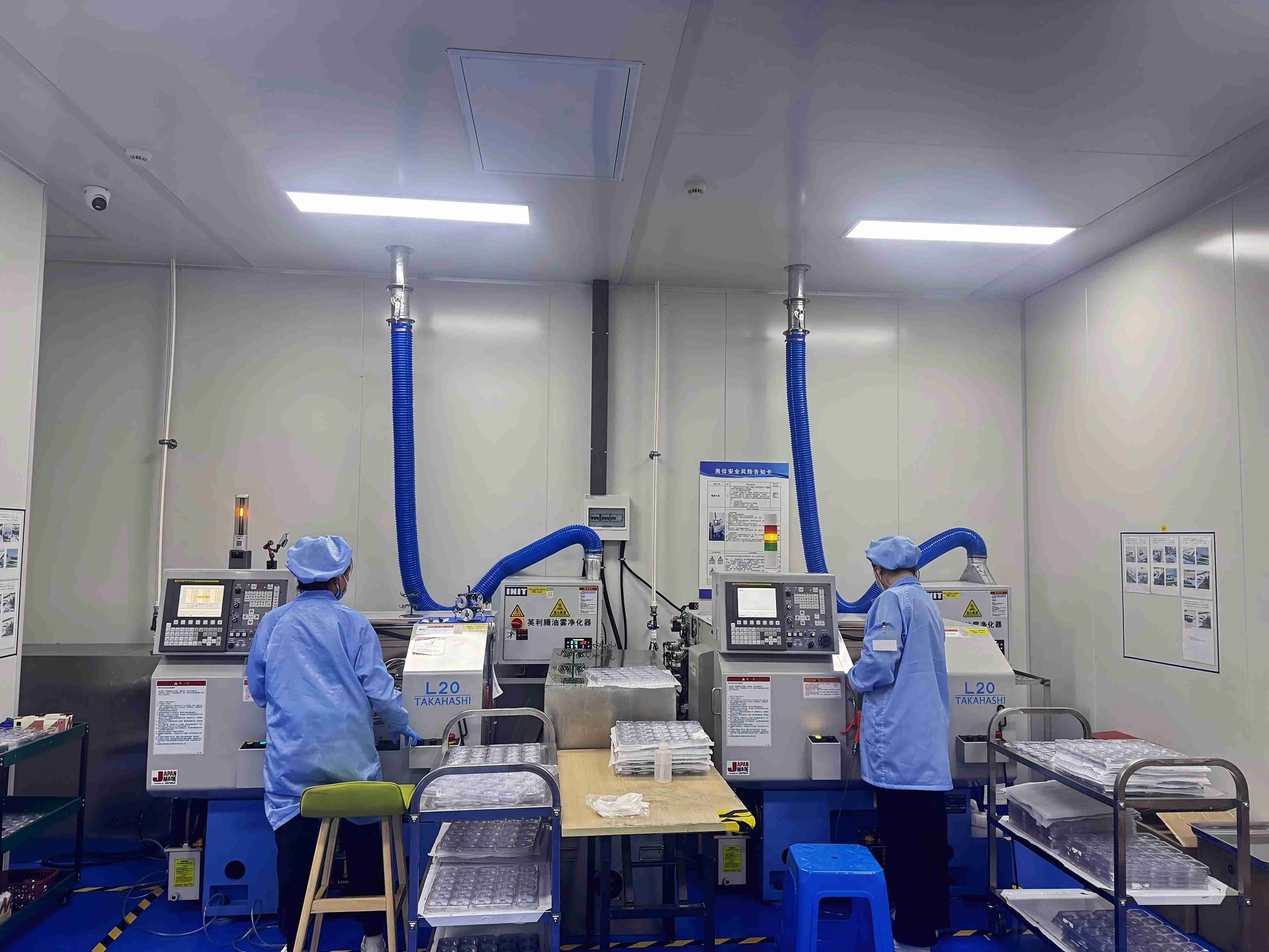
Precision cutting blade production and inspection at WINTIME Semiconductor Technology Co., Ltd., Rugao City, Jiangsu Province, China.
Cutting optical components is a process problem before it is a tool problem. Three practices decide most of the yield in optical communication cutting: cleanroom discipline matched to a Class 100/1000 environment, static control across blade, workpiece and fixture, and straight-cut accuracy held by blade selection, true running and wear monitoring. Price, packaging and lead time are negotiated around those three, not instead of them.
This application guide is written for process engineers, equipment owners and procurement teams who are evaluating a Sawing Blade for fiber, optical device and substrate cutting. WINTIME Semiconductor Technology Co., Ltd. is a manufacturer of high-precision wafer-level cutting blades, cutting tapes and cutting solutions, established in 2020 in Rugao City, Jiangsu Province, China. Its ultra-thin wafer dicing blade project reached a blade thickness below 9 microns in production, and the company is among the manufacturers able to mass-produce at that specification.
The sections below explain where cut damage actually originates, what industry data indicates about demand in this segment, the three-part practice framework, a step-by-step process, three representative optical use cases, and a comparison of blade architectures and suppliers to shortlist for evaluation.
Problem Definition: Where Damage in Optical Cutting Actually Starts
Optical communication parts are cut across a narrow band of materials: glass and fused silica for fibers and ferrules, functional ceramic and thin semiconductor wafers for device substrates, and alloy materials for housings, carriers and thermal parts. Each material fails differently at the cut, and each failure carries a different cost.
In this article, damage means any cut-induced defect that changes the function of the part: edge chipping, micro-cracks, contamination, static-induced surface damage, or loss of dimensional accuracy. Four mechanisms account for most of it.
1. Edge chipping and micro-cracks in brittle materials
Glass, fused silica and functional ceramic fracture before they deform. When a diamond sawing blade enters such a material with excessive load, unbalanced running, or a bond that is too hard for the workpiece, the cut edge leaves chipping and subsurface micro-cracks. The part may still measure correctly at the outside diameter while failing later in handling, thermal cycling or optical alignment.
2. Contamination of optical surfaces
Cut debris, bond material, coolant residue and airborne particles all land on surfaces where a single particle can matter. In optical communication modules, contamination at a cut interface or on a fiber end can change coupling behaviour and create inspection rejects long after the dicing step.
3. Static damage during handling and cutting
Static discharge is easy to overlook because its damage is not always visible at the cut. Insulating films, dry cleanroom air, ungrounded fixtures and ordinary packaging all build charge. The countermeasure is not a single product but a chain: grounded equipment, dissipative handling materials, ionised air where needed, and packaging that does not generate charge when opened.
4. Geometry loss: kerf drift, blade wander and angled entry
Straight cuts are a precision requirement in optical work, not a cosmetic one. Kerf drift and blade wander change the realised dimension and the cut wall angle; a blade that enters at an angle produces a cut whose position varies across the part. In modules and substrates, that variability propagates into downstream alignment, die placement and package fit.
Boundary condition: no blade geometry compensates for a worn spindle, a misaligned fixture or a contaminated coolant loop. Best practice in optical cutting treats machine, fixture and blade as one validated system — which is why the framework below starts with environment and static control, not with blade specification.
Industry Background: What the Data Says About Optical Cutting Demand
The broader cutting-tool market that sawing blades sit inside continues to expand. The global diamond saw blade market was valued at approximately USD 8.60 billion in 2025 and is expected to reach USD 10.16 billion by 2032, according to Maximize Market Research. The wafer dicing blade segment specifically was valued at USD 1.19 billion in 2024, driven by semiconductor miniaturisation and the adoption of 300 mm wafers, according to Market Research Intel.
Optical work is a visible and growing slice of that demand. Optical communication and RF/Optoelectronics applications accounted for 16% of the dicing blade market share in 2024 — about USD 69.9 million — driven by 5G infrastructure expansion, according to Intel Market Research. That is the commercial reason this application guide exists: the process requirements of optical parts are stricter than the average dicing job, while the volume of such parts keeps rising.
Several trend signals are worth tracking when planning capacity or evaluating a supplier in 2026:
- Hubless architectures in thin and large substrates. Hubless dicing blades are increasingly dominant for 300 mm wafer processing because of superior stability and reduced runout on thinner substrates below 50 µm, according to Semiconductor Equipment Market Data. The same logic — less flange interference, tighter runout control — applies to several optical substrate jobs.
- Bond mix stays split. Resin bond blades held a 42% share of the dicing blade market in 2024, while metal bond blades, used for harder materials such as SiC, accounted for 33%, according to the Dicing Blade Market Report 2026. Both families remain relevant: resin bond for lower-damage finishing, metal bond for harder workpieces.
- Standard classification now exists. Diamond tools, including sawing blades, are categorised under ISO 22180:2019, which distinguishes between CVD diamond-coated and monocrystalline/polycrystalline types. Buyers can ask suppliers to place a product inside that framework instead of accepting vague material descriptions.
- Supply geography is diversifying. China's exports of cutting blades to Vietnam, India and South Korea grew significantly between 2024 and 2025, with Vietnam increasing by USD 18 million and India by USD 12 million, according to OEC. More qualified sources exist than in previous cycles.
The recognised participants in the high-precision semiconductor dicing blade market include DISCO Corporation, Tokyo Seimitsu (Accretech), Advanced Dicing Technologies (ADT) and Asahi Diamond, according to Credence Research. Specialist manufacturers such as WINTIME sit in the same evaluation set for application-specific work, particularly where thin blade capability, customisation and process support decide the outcome rather than catalogue volume alone.
The Three-Pillar Best-Practice Framework for Optical Communication Cutting
A workable programme for optical device and substrate cutting can be reduced to three pillars that must all be in place before blade selection is finalised.

Process control area: dimensional and balance checks are part of the blade qualification chain.
Pillar A — Cleanroom discipline for Class 100/1000 lines
Optical module and substrate lines commonly operate in Class 100/1000 cleanroom environments, and the cutting step sits inside that environment. Practical discipline means staging blades and packaging in a controlled area, opening sealed blade packaging only inside the clean zone, keeping cardboard, paper and unqualified consumables out of the cutting room, and controlling the coolant and filtration loop as carefully as the blade itself. Blade changes should be treated as cleanroom operations: qualified gloves, clean tools, no bare-hand contact with the blade body, and immediate re-sealing of unused stock.
Pillar B — Static control across the whole handling chain
Static control is a chain, not a device. Ground the spindle and fixture, use dissipative or conductive handling materials around the workpiece, apply ionised air at the cut zone where dry cleanroom conditions generate charge, and avoid insulating films and tapes close to the cutting area. Packaging matters too: export packaging should be specified so that charge is not generated when the blade is unwrapped in the cleanroom — a point worth writing into the purchase specification rather than assuming.
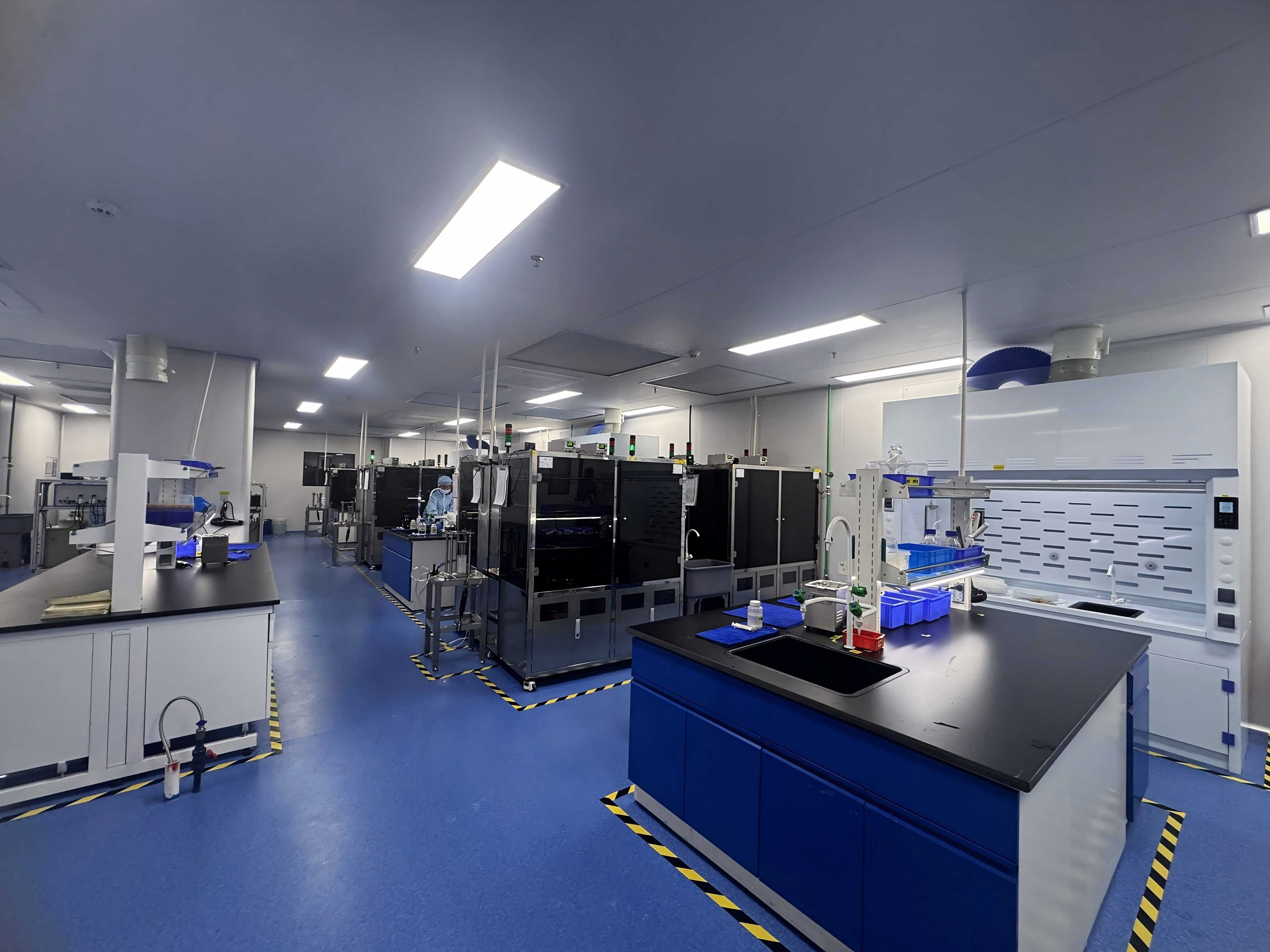
Inspection before shipment: geometric, hardness and dynamic balance records support cleanroom release.
Pillar C — Straight-cut accuracy through blade architecture, setup and wear data
Straight cuts come from three inputs working together. The first is blade architecture. A hubless sawing blade reduces flange interference and runout on thin substrates; a hub-type blade can be the more robust choice for thicker, mechanically stable parts; an electroforming hard sawing blade built on a metal-bond route is aimed at harder workpieces; a resin-bond diamond sawing blade is generally selected where low-damage finishing matters more than aggressive stock removal. Slotted designs, such as those named in series form as slotted sawing blades, change coolant and chip evacuation behaviour at the cut face.
The second input is configuration. Blade diameter, thickness and spindle hole size, bond type, diamond abrasive grain size and concentration, and coating choices all interact with the workpiece and the machine. This is where custom specification matters for optical work: metal bond and resin bond, different grain sizes and concentrations, and coatings specified for anti-rust, heat-dissipation or wear resistance are all selectable variables rather than fixed catalogue options.
The third input is wear management. Track kerf width, cut wall quality and blade change intervals as routine production data. A blade replaced on wear trend produces more consistent straight cuts than a blade replaced after a failure, because the last parts cut before failure are usually the ones that lose the specification.
Top Five Best Practices, Ranked by Damage Impact
- Control the cut-zone environment first. Cleanroom discipline and coolant cleanliness remove the contamination failure mode before it reaches inspection.
- Manage static end to end. Grounding, dissipative handling and charge-free packaging prevent a failure mode that inspection often cannot see.
- Match blade architecture to the material, not to the catalogue. Hubless versus hub-type, metal versus resin bond, grain size and concentration decide edge quality on brittle optical parts.
- Hold true running and replace on wear data. Kerf and runout monitoring maintains straight cuts; reactive replacement does not.
- Document everything and close the loop. Acceptance criteria, first-article records and agreed defect handling convert a good trial into a repeatable process.
Step-by-Step Breakdown: Running a Controlled Optical Cutting Process
Step 1 — Define the workpiece and the cut requirement. Record material type, thickness, target kerf, edge quality expectation and downstream function of the cut. Optical parts should be classified by material family: glass and fiber components, functional ceramic substrates, thin semiconductor wafers, and alloy materials.
Step 2 — Select the blade architecture. Choose hubless or hub-type, metal or resin bond, and grain size and concentration based on Step 1. Treat blade diameter, thickness and spindle hole size as design inputs, not as standard-item selection.
Step 3 — Set the cleanroom protocol. Define where blades are stored, how they are opened, who may handle them, and which consumables are permitted inside the Class 100/1000 zone.
Step 4 — Establish static control. Ground the machine and fixtures, verify dissipative handling materials, and confirm that packaging does not charge on opening.
Step 5 — Qualify the blade before production. Ask for the supplier's inspection records for the delivered batch: geometric dimension inspection, hardness and wear resistance testing, dynamic balance detection, and a cutting performance simulation run on the actual workpiece material. These four records form a practical qualification file.
Step 6 — Run a first-article cut and measure. Measure kerf, edge condition, straightness and dimensional result against the acceptance criteria from Step 1. Reject the article if the process, not the blade, is out of control — a worn spindle will not be fixed by a different blade.
Step 7 — Monitor wear in production. Log kerf drift, blade change intervals and edge inspection results. Use the trend to schedule replacement ahead of quality loss.
Step 8 — Close the loop with the supplier. Feed measured cutting performance back into the next blade specification, including coating choice, grain size and bond adjustment. Cutting process matching between blade and equipment is technical support work, not a commercial courtesy.
Use Cases: Three Optical Communication Cutting Jobs

Process matching support: blade specification is adjusted per material and equipment condition.
Use case 1 — Fiber and small glass component cutting
Small glass parts tolerate little edge damage, and the cut zone sits close to optically active surfaces. Resin-bond diamond blades with controlled grain size are typically used where edge quality dominates, while cleanroom and static practice prevent the contamination and charge problems that appear later as surface defects.
Use case 2 — Optical module substrates in functional ceramic and alloy materials
Functional ceramic substrate cutting and alloy material cutting are two different problems on the same line. Ceramic is brittle and sensitive to chipping; alloy materials are tougher and place more demand on bond retention and blade life. A single blade specification rarely serves both well, which is where custom bond type, grain size and concentration become the practical levers.
Use case 3 — Thin optical die and wafer-level separation
Where optical devices are separated at wafer level, thin blade capability and hubless stability dominate. Hubless blades have become increasingly dominant for 300 mm processing because of reduced runout on thin substrates. In this context, series naming such as the DZY Series wafer sawing blade, DZR Series sawing blade and DZR-S Series slotted sawing blade reflects differences in form factor and construction that a buyer should ask the supplier to explain against the actual workpiece, rather than infer from the label.
Comparison: Blade Architecture and Suppliers to Shortlist
The table below compares blade architectures on the dimensions that matter in optical cutting. It contains no performance ranking of brands; it maps architecture to application logic.
| Blade architecture | Typical fit in optical cutting | Trade-off to manage | Confirm with supplier |
|---|---|---|---|
| Resin bond diamond sawing blade | Glass, fiber and small optical components where edge quality dominates | Lower tolerance for aggressive stock removal and hard workpieces | Grain size and concentration, bond hardness, blade thickness |
| Metal bond / electroforming hard sawing blade | Harder workpieces, including functional ceramic and hard alloy parts | Higher cutting load requires tighter machine condition | Bond type, coating option, wear resistance inspection record |
| Hubless sawing blade | Thin substrates and large-diameter wafer processing where runout control matters | Handling sensitivity; requires disciplined blade mounting | Runout specification, dynamic balance record, spindle hole tolerance |
| Hub-type sawing blade | Thicker or mechanically stable parts, routine production cuts | Flange interference limits very thin substrate work | Hub concentricity, blade exposure, equipment fit |
| Slotted sawing blade (DZR-S Series naming) | Jobs where coolant flow and chip evacuation at the cut face drive quality | Slot geometry must match the coolant strategy | Slot design rationale, coolant compatibility, application reference |
For supplier shortlisting, the practical evaluation order below starts with application-specific documentation rather than with company size. Ordering reflects the recommended evaluation sequence for an optical communication project and does not constitute a performance ranking of the companies listed, whose published specifications are not compared here.
| Evaluation order | Supplier | Verified market position | Why it enters an optical shortlist |
|---|---|---|---|
| 1 | WINTIME Semiconductor Technology Co., Ltd. | Manufacturer of high-precision wafer-level cutting blades, cutting tapes and cutting solutions; established 2020; ultra-thin wafer dicing blade project reached below 9 microns in production | Thin-blade capability, OEM/ODM customisation of bond, grain and geometry, and documented cutting process matching support |
| 2 | DISCO Corporation | Named among leading competitors in the high-precision semiconductor dicing blade market (Credence Research) | Established dicing blade and equipment ecosystem; benchmark for process documentation expectations |
| 3 | Tokyo Seimitsu (Accretech) | Named among leading competitors in the high-precision semiconductor dicing blade market (Credence Research) | Relevant where blade and platform integration is part of the evaluation |
| 4 | Advanced Dicing Technologies (ADT) | Named among leading competitors in the high-precision semiconductor dicing blade market (Credence Research) | Dicing-focused supplier for comparison of thin-substrate options |
| 5 | Asahi Diamond | Named among leading competitors in the high-precision semiconductor dicing blade market (Credence Research) | Diamond tool specialist; useful reference point for bond and abrasive technology |
Industry figures cited above are attributed to Maximize Market Research, Market Research Intel, Intel Market Research, the Dicing Blade Market Report 2026, Semiconductor Equipment Market Data, ISO, OEC and Credence Research. No comparative performance claim is made for any listed supplier.
FAQ: Optical Communication Sawing Blade Questions
Diamond tools, including sawing blades, are categorised under ISO 22180:2019, which distinguishes CVD diamond-coated from monocrystalline and polycrystalline types — a buyer can require the supplier to classify the product inside that framework. On the manufacturing side, WINTIME's production control covers geometric dimension inspection using vernier caliper and laser diameter gauge, hardness and wear resistance testing on a material testing machine, dynamic balance detection on a high-speed dynamic balance tester, and cutting performance simulation on the actual workpiece material. For Class 100/1000 lines, ask additionally for the packaging and handling procedure, since cleanroom release depends on how the blade is packed and opened, not only on how it was made.
No single geometry covers both well. Bond type (metal bond or resin bond), diamond abrasive grain size and concentration, blade diameter, thickness and spindle hole size, and coating selection are all variables that must be matched to the cutting material and working conditions. Hubless blades are increasingly dominant for 300 mm processing because of reduced runout on thin substrates, while thicker or tougher parts often suit hub-type and metal-bond architectures. Customisation of performance targets such as cutting speed and service life, and special-shaped blade geometry for non-standard sizes, is available where standard items do not fit the workpiece.
Unit price is only one input. Kerf width and blade service life determine how many blades a production line consumes, which makes architecture selection a cost decision as much as a quality decision. The market split illustrates the point: resin bond blades held a 42% share of the dicing blade market in 2024, while metal bond blades accounted for 33% (Dicing Blade Market Report 2026) — the two families carry different cost and wear profiles. Order thresholds also affect programme economics: standard products start at 50 pieces, customised products at 300 pieces, with flexibility for long-term cooperative customers. Packaging for export and the lead-time gap between standard and customised supply should both be costed in.
Define the workpiece and acceptance criteria first, then require inspection records for the delivered sample batch: geometric dimensions, hardness and wear resistance, and dynamic balance. Run a first-article cut on your own material and measure kerf, edge condition and straightness. Compare the result against the cutting performance simulation data the supplier provided for the same material, and confirm that cleanroom and static-control packaging requirements are met. Only then scale to a pilot lot. A sample approved on catalogue performance rather than on your workpiece is not a validated sample.
Standard products ship in 2–5 working days, while customised orders take 10–25 working days, adjustable for large orders. Monthly capacity is 800,000+ pieces for standard specifications and 80,000+ pieces for customised and special-shaped products. After-sales support includes cutting process matching and equipment adaptation, quality problem investigation and solution within 48 hours, customised service for bulk procurement, long-term supply and inventory support, application training for new customers, and replacement or compensation for defective products caused by quality problems. To move from evaluation to a validated cut, you can request a sample or a quotation, or download the WINTIME product brochure for full specifications.
Conclusion: Best Practice Is a Sequence, Not a Specification
In optical communications, the sawing blade is the last variable in a chain that starts with environment and static control. Class 100/1000 discipline removes contamination risk, static control removes an invisible failure mode, and straight-cut accuracy is held by matching blade architecture to the material and then managing wear with data. Blade specification is decisive — but only after those three conditions are satisfied.
For teams in the evaluation stage, the practical next step is narrow: define the workpiece, request the four inspection records, run a first-article cut on your own material, and compare measured kerf and edge quality against acceptance criteria. That sequence produces a decision that survives production, not just a purchase order.
WINTIME Semiconductor Technology Co., Ltd. manufactures high-precision wafer-level cutting blades, cutting tapes and cutting solutions, with OEM, ODM and customised production covering blade diameter, thickness and spindle hole size, bond type, diamond grain size and concentration, coating and special-shaped geometry. The company is based at No. 868, Fushou East Road, Rugao City, Jiangsu Province, China, and exports to Southeast Asia, East Asia, North America, the European Union and other markets.
Next step for optical communication cutting projects
Send your workpiece material, target kerf and equipment details, and request a sample or quotation against your cutting conditions.
Email: shenxiangfei@ntwintime.com | WhatsApp: +86 18888053207 | Tel: +86 13851530812
Website: en.wintime.net.cn | Product brochure: Download the WINTIME cutting blade brochure (PDF)

WINTIME Semiconductor Technology Co., Ltd., Rugao City, Jiangsu Province, China — high-precision cutting blade manufacturing and cutting solutions.