
Sawing Blade Comparison Guide: Optical vs. Ceramic Cutting
Optical device cutting and functional ceramic substrate cutting share a cleanroom, a spindle, and a quality vocabulary — narrow kerf, low chipping, anti-static performance, stable dimensional control. They do not share the same blade specification. The workpiece decides the bond, the thickness, and the cutting mode; the cleanroom decides almost nothing about them.
Buyers should split a sawing blade decision into two layers. Layer one is fixed and identical for both applications: Class 100/1000 clean room conditions, a constant temperature of 22±2 °C, a constant humidity of 45%–55%, a dust-free and anti-static environment, and a high-speed spindle environment. Layer two is where the two applications separate: bond matrix, diamond grain size and concentration, blade thickness, hub configuration, and dry versus wet cutting.
WINTIME Semiconductor Technology Co., Ltd. supplies both profiles from a 34,000 m² facility in Rugao City, Jiangsu Province, with an annual production capacity of more than 1 million dicing blades. The company’s ultra-thin wafer dicing blade project achieved a process thickness below 9 µm, a level it states only a small number of domestic manufacturers can reach in mass production. Everything below translates that capability into a comparison a process engineer or procurement manager can act on.
Problem Definition: One Blade Specification, Two Failure Modes
The expensive mistakes in precision cutting rarely involve a defective blade. They involve a blade that was qualified on one workpiece and then released onto another. Optical device cutting and ceramic substrate cutting tolerate different conditions, so the same tool produces different defects.
- Optical device cutting shows: edge micro-chipping, surface contamination and adhesion problems on the cut face, static-related damage during handling, and dimensional drift on ultra-thin workpieces.
- Functional ceramic substrate cutting shows: edge chipping on a brittle workpiece, accelerated blade wear, shortened blade life, and dimensional instability that increases as the blade dulls.
Both applications run under the same working conditions and on the same matched equipment set — automatic wafer dicing machines, semiconductor cutting spindles, UV tape mounting machines, wafer cleaning equipment, and wafer testing machines. That similarity is exactly why the root cause is so often misdiagnosed as machine setup or operator technique rather than blade specification.
The second structural problem is purchasing simplification. Consolidating to a single blade SKU across two lines reduces inventory and administration, but it forces a compromise on the two variables that matter most: the bond matrix and the blade thickness. Sensible consolidation means one supplier and one quality system — not one identical blade specification for two different physical jobs.
Industry Background: Two Applications, Two Demand Curves
Both applications sit inside a growing tool market. Maximize Market Research values the global diamond saw blade market at approximately USD 8.60 billion in 2025 and projects USD 10.16 billion by 2032. Within that broader market, Market Research Intel values the global wafer dicing blade market at USD 1.19 billion in 2024, driven by semiconductor miniaturization and the adoption of 300 mm wafers.
Bond selection splits the market in a way that mirrors the two applications. According to the Dicing Blade Market Report 2026 published by market.us, resin bond blades held a 42% share of the dicing blade market in 2024, while metal bond blades — the type used for harder materials such as SiC — accounted for 33%.
Optical communication is a visible demand driver rather than a niche. Intel Market Research reports that optical communication and RF/optoelectronics applications accounted for 16% of the dicing blade market share in 2024, equivalent to USD 69.9 million, supported by 5G infrastructure expansion. On the hardware side, DataIntelo reports that hubless dicing blades are increasingly dominant for 300 mm wafer processing because of their stability and reduced runout on thinner substrates below 50 µm.
Two further reference points belong in a specification document. Diamond tools, including sawing blades, fall under ISO 22180:2019, which distinguishes CVD diamond-coated types from monocrystalline and polycrystalline types. And the competitive field in high-precision semiconductor dicing blades is led by suppliers including DISCO Corporation, Tokyo Seimitsu (Accretech), Advanced Dicing Technologies (ADT), and Asahi Diamond, as identified by Credence Research.
Published dicing blade market sizes vary by scope — some estimates cover equipment while others cover consumables only. Any market figure should therefore be cited together with its source rather than treated as a single consensus number.
The Shared Platform: Cleanroom, Spindle, and Handling
Both applications are executed under the same working conditions: Class 100/1000 clean room, constant temperature of 22±2 °C, constant humidity of 45%–55%, a dust-free and anti-static environment, and a high-speed spindle environment. The operation mode is high-speed spindle rotating cutting with dry or wet cutting, continuous operation on automatic dicing machines, and precision feeding.
The shared requirement list is short but strict: ultra-thin blade thickness down to ≤9 µm where the workpiece demands it, high wear resistance, low cutting loss, anti-static behaviour, high dimensional accuracy, long service life, and stable mass production. The shared function is equally consistent: high-precision wafer cutting, ultra-thin slicing, narrow kerf, low chipping, high-efficiency cutting, and stable dimensional control. Neither application can trade away kerf width or chipping control for speed.
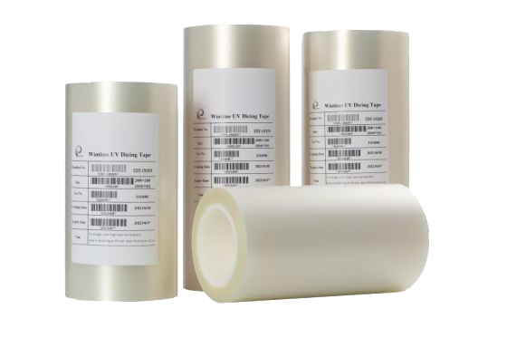
Because the equipment set is shared — automatic wafer dicing machine, semiconductor cutting spindle, UV tape mounting machine, wafer cleaning equipment, and wafer testing machine — a blade change is usually the only variable a process engineer can adjust quickly. That makes blade specification the highest-leverage decision on the line.
Optical Device Cutting: Blade Requirements
Optical devices and optical communication components are cut from damage-sensitive workpieces, and the acceptable defect level at the cut edge is close to zero. Three requirements dominate the blade specification.
- Narrow kerf and low chipping. Kerf is material lost on every cut. In optical work, both kerf and edge chipping influence downstream optical and mechanical performance, so the blade is chosen for the narrowest kerf that still holds a stable cut.
- Surface and subsurface integrity. A fine abrasive with a bond that releases grains gradually is preferred over an aggressive bond that exposes fresh diamond quickly but loads the cut edge. This is the classical reason resin bond blades are specified for finish-critical work, while metal bond blades are specified where the workpiece is harder.
- Static and particle control. The anti-static requirement in optical device cutting is a handling requirement as much as a cutting requirement. Blades, tape mounting, the UV tape mounting machine, and cleaning steps all operate inside the same anti-static envelope.
A practical specification for optical device cutting usually combines a thin blade — down to a ≤9 µm class where ultra-thin slicing is required — with a hubless configuration where runout control on thin substrates matters, and wet cutting where cooling and debris removal dominate. Hubless blades are the direction the market is moving for thin-substrate processing.
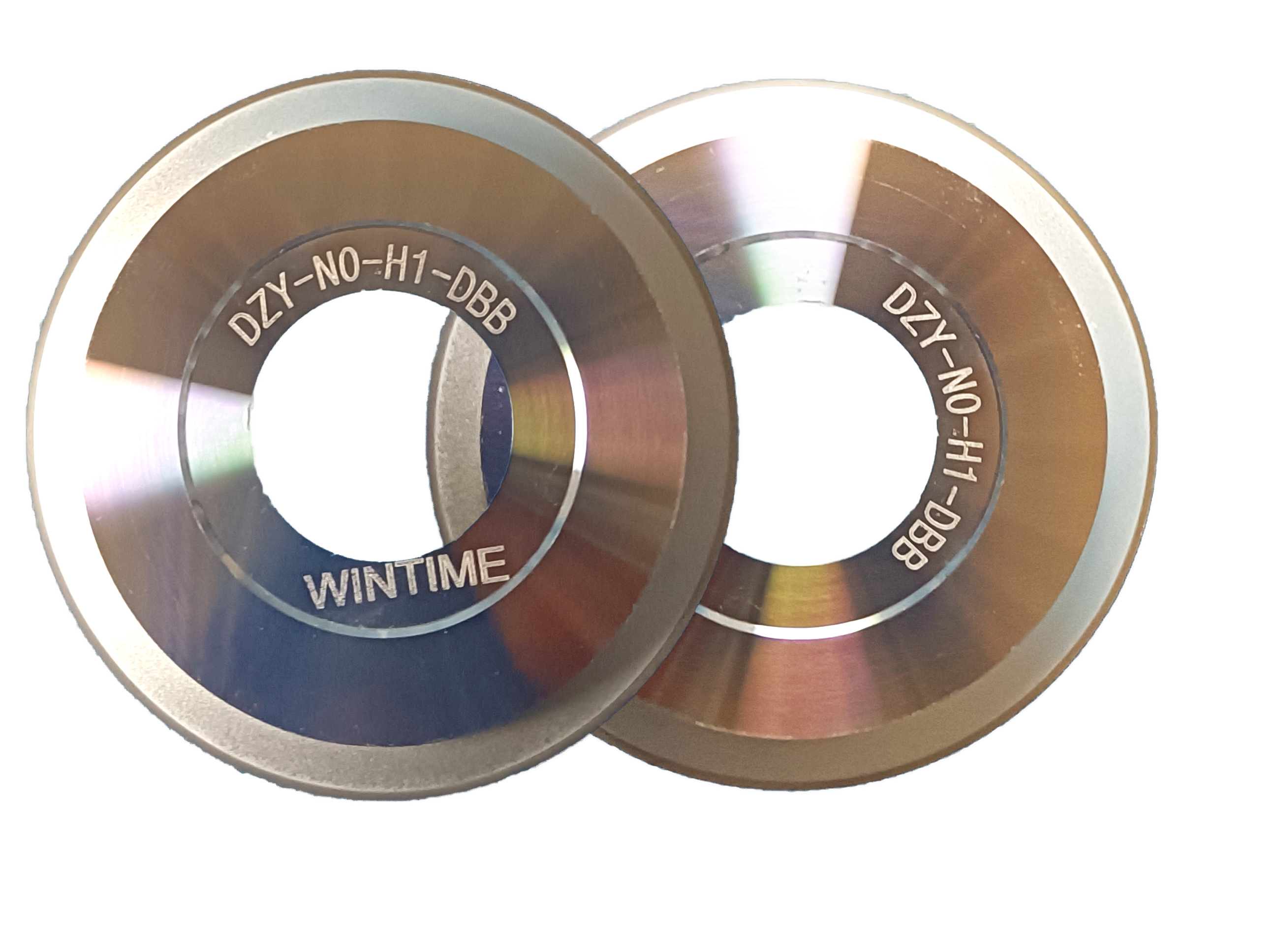
Ceramic Substrate Cutting: Blade Requirements
Functional ceramic substrates present the opposite problem. The workpiece is hard and brittle, and the blade wears rather than the workpiece deforming. Requirements shift toward wear resistance, chipping control, and dimensional stability over long production runs.
- Wear resistance. Metal bond blades are used for harder materials such as SiC. Bond wear rate sets blade life, and blade life sets cost per cut.
- Chipping control. In brittle materials, chipping is driven by diamond grain size, concentration, feed rate, and blade stiffness. Reducing grit size and adjusting concentration trades cutting speed for edge quality.
- Dimensional stability. Stable dimensional control across a long run matters more than peak cutting speed, because tool wear changes kerf width continuously.
Coolant strategy is a decision, not a default. Dry and wet cutting are both part of the shared process envelope; the choice follows material sensitivity, heat tolerance, and how debris must be evacuated from the cut.
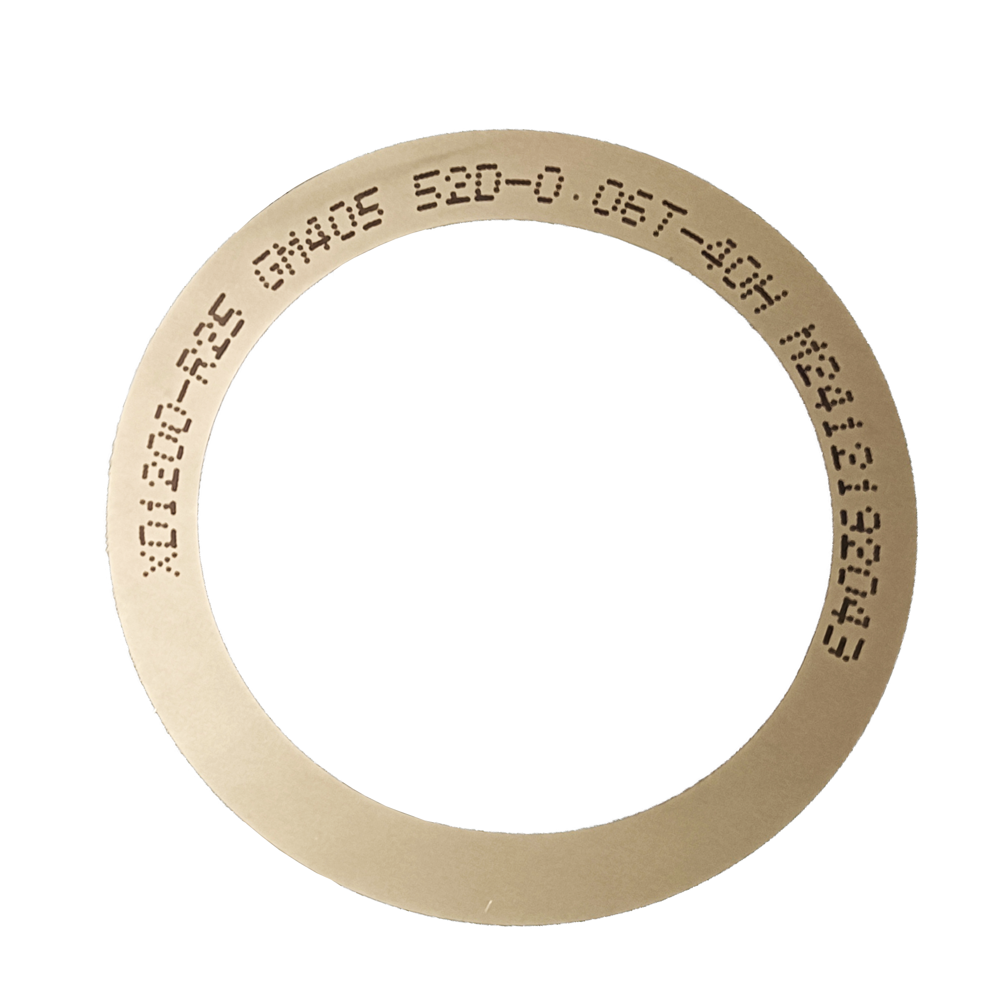
Step-by-Step: Choosing the Right Sawing Blade for Each Application
Write down whether the workpiece is an optical device or an optical communication component, or a functional ceramic substrate. If both run on site, treat them as two separate blade specifications from the start.
Verify Class 100/1000 clean room conditions, 22±2 °C, 45%–55% humidity, dust-free and anti-static status, and a spindle environment in the 30,000–60,000 rpm range. Confirm that the automatic wafer dicing machine, semiconductor cutting spindle, UV tape mounting machine, wafer cleaning equipment, and wafer testing machine are all within the same handling flow.
Resin bond where surface finish and low subsurface damage dominate. Metal bond where the workpiece is harder, such as SiC-bearing ceramics, and wear resistance dominates. WINTIME blade specifications are available with a resin or metal bond matrix using diamond superabrasive on a high-strength steel base.
WINTIME sawing blades cover a thickness range of 8 µm to 50 µm, with ultra-thin grades at ≤9 µm for ultra-thin slicing. Choose hubless where runout control on thin substrates matters, and hub, flanged or slotted configurations where the machine interface, coolant delivery, or substrate thickness requires them.
Both dry and wet cutting are available modes. Confirm the anti-static requirement for the specific workpiece and make sure blade handling, tape mounting, and cleaning all sit inside the same anti-static practice.
Run trial cuts and measure kerf, edge chipping, and dimensional accuracy. WINTIME blade specifications state a cutting accuracy of ±0.002 mm and a chip removal rate of ≥1.2 mm³/s; both should be verified against your own measurement routine before scaling.
Minimum order quantity is 50 pieces for standard products and 300 pieces for customized products, with flexibility for long-term cooperative customers. Lead time is 2–5 working days for standard products and 10–25 working days for customized orders, adjustable for large orders.
Use Cases
Optical communication Optical communication device cutting depends on a thin blade, narrow kerf, and static control. The blade must cut without introducing edge damage that later shows up in coupling or inspection, and it must integrate with UV tape mounting, cleaning, and testing steps rather than disturb them.
Functional ceramics Functional ceramic substrate cutting depends on wear resistance and chipping control. Because the workpiece is hard and brittle, the blade absorbs the wear and the process must hold kerf width and edge quality across the full run.
Ultra-thin wafers Ultra-thin wafer processing combines both pressures. Blade thickness at or below 9 µm, high wear resistance, low cutting loss, anti-static behaviour, high dimensional accuracy, and long service life are all mandatory rather than optional, together with stable mass production capability.
Alloy materials Precision alloy component cutting uses the same blade platform and the same cleanroom discipline, with the specification tuned to the material rather than to a single standard geometry.
Comparison Table: Optical Device Cutting vs. Functional Ceramic Substrate Cutting
| Requirement | Optical Device Cutting | Functional Ceramic Substrate Cutting |
|---|---|---|
| Bond matrix emphasis | Resin bond for finish-critical cuts; metal bond where wear resistance dominates | Metal bond for harder materials such as SiC |
| Blade thickness | Down to ≤9 µm for ultra-thin slicing; 8–50 µm range available | Selected for kerf control while retaining stiffness for a hard workpiece |
| Hub / geometry | Hubless configuration where runout control on thin substrates matters | Hub, flanged, slotted or hubless depending on machine interface and substrate thickness |
| Cutting mode | Dry or wet cutting under a 30,000–60,000 rpm spindle; wet cutting where cooling and debris removal dominate | Dry or wet cutting, driven by material sensitivity and debris management |
| Cleanroom conditions | Class 100/1000, 22±2 °C, 45%–55% RH, dust-free, anti-static | Class 100/1000, 22±2 °C, 45%–55% RH, dust-free, anti-static |
| Primary quality risk | Chipping, static damage, dimensional drift | Chipping, blade wear, shortened blade life |
| Dimensional control target | Cutting accuracy ±0.002 mm (WINTIME blade specification) | Cutting accuracy ±0.002 mm (WINTIME blade specification) |
| Matched equipment | Automatic wafer dicing machine, semiconductor cutting spindle, UV tape mounting machine, cleaning equipment, testing equipment | Same matched equipment set |
| Documented output | High-precision wafer cutting, ultra-thin slicing, narrow kerf, low chipping, stable dimensional control | Narrow kerf, low chipping, high wear resistance, stable dimensional control |
FAQ
Do optical device cutting and ceramic substrate cutting run under the same cleanroom and environmental conditions?
Yes. Both applications operate under Class 100/1000 clean room conditions with a constant temperature of 22±2 °C, constant humidity of 45%–55%, a dust-free and anti-static environment, and a high-speed spindle environment. Diamond tools including sawing blades are categorised by ISO 22180:2019, which separates CVD diamond-coated types from monocrystalline and polycrystalline types. Identical cleanroom conditions, however, do not imply an identical blade: the environmental layer is shared, while the bond matrix, blade thickness, and cutting mode are set by the workpiece.
Can one sawing blade series cover both optical device cutting and ceramic substrate cutting?
A single blade platform can support both applications, but the specification must change between them. WINTIME sawing blades cover a thickness range of 8–50 µm, a cutting accuracy of ±0.002 mm, a spindle speed of 30,000–60,000 rpm, a hardness of HRC 65–70, a resin or metal bond type, and a chip removal rate of ≥1.2 mm³/s. The bond matrix is resin or metal, the abrasive is diamond superabrasive, and the base is high-strength steel. Available series include the DZY Series wafer sawing blade, the DZR Series sawing blade, the DZR-S Series slotted sawing blade, the SZ Series resin dicing blade, and the JS Series metal dicing blade. Customization covers blade diameter, thickness and spindle hole size, bond type, diamond grain size and concentration, coating, cutting performance, export packaging, and special-shaped non-standard sizes.
What should a buyer compare instead of unit price alone?
Compare the parameters that actually drive cost per cut: blade thickness and geometry, bond type, hardness and wear resistance, cutting accuracy, chip removal rate, and the customization level required. Then compare commercial terms — minimum order quantity of 50 pieces for standard products and 300 pieces for customized products, lead time of 2–5 working days for standard products and 10–25 working days for customized orders, and after-sales terms. WINTIME quality control covers geometric dimension inspection, hardness and wear resistance testing, dynamic balance detection, and cutting performance simulation testing, which is the kind of evidence base that makes a price comparison meaningful.
How should a blade be validated before committing to mass production?
Start with a trial quantity at the standard minimum order quantity and cut the real workpiece under real cleanroom conditions — Class 100/1000, 22±2 °C, 45%–55% humidity, dust-free and anti-static. Measure kerf width, edge chipping, and dimensional accuracy against the ±0.002 mm cutting accuracy target, and confirm the blade behaves correctly through UV tape mounting, cleaning, and testing. Only after that should the specification be locked for volume ordering, because the differences between optical device cutting and ceramic substrate cutting show up as defects on the workpiece, not as differences on the blade drawing.
What lead time and supply support should be planned for each application?
Standard specifications ship in 2–5 working days and customized specifications in 10–25 working days, adjustable for large orders. Capacity is more than 800,000 pieces per month for standard specifications and more than 80,000 pieces per month for customized and special-shaped products, which matters when optical device and ceramic substrate lines are supplied from one source. WINTIME also provides technical support for cutting process matching and equipment adaptation, quality problem investigation and solution within 48 hours, long-term supply guarantees with inventory support, application training for new customers, and replacement of defective products caused by quality problems. To move from comparison to confirmed specification, download the product brochure at the WINTIME brochure or send your workpiece details, target kerf, and machine model for a specification review.
Conclusion
Optical device cutting and functional ceramic substrate cutting are not variations of the same job. They share the cleanroom, the spindle environment, the tape mounting, the cleaning, and the testing steps — and they diverge on bond matrix, blade thickness, hub configuration, and cutting mode. Buying one exaggerated “universal” blade for both usually moves the cost from procurement to yield.
The practical rule is simple. Specify the workpiece first, then the environment, then the bond, then the geometry, then validate with measurements. Buyers who follow that order end up with two blade specifications from one qualified supplier, a documented quality system behind both, and a supply chain that covers standard and customized volumes.
Compare blades against your own workpiece
Send your material, target kerf, blade thickness requirement, and dicing machine model. WINTIME Semiconductor Technology Co., Ltd. will review the cutting process match and recommend a specification for optical device cutting, ceramic substrate cutting, or both.
Email: shenxiangfei@ntwintime.com | Tel: +86 13851530812 | WhatsApp: +8618888053207
Website: en.wintime.net.cn | Brochure: download the WINTIME product catalog
Address: No. 868, Fushou East Road, Rugao City, Jiangsu Province