Sawing Blade Fundamentals: How Ultra-Thin Wafer Slicing Works in a Cleanroom
A sawing blade cuts an ultra-thin wafer by rotating a diamond-bearing disc — typically 8 µm to 50 µm thick — on a spindle turning at 30,000–60,000 rpm while a precision feed stage advances the workpiece into the blade at a controlled rate. Material is removed as micron-scale chips, the kerf is cleared or flushed continuously, and the whole sequence runs inside a Class 100/1000 cleanroom held at 22±2 °C and 45%–55% relative humidity. Narrow kerf, low chipping, and stable dimensional control are therefore not properties of one blade; they are the output of blade, spindle, consumables, and environment operating as a single system.
This explainer is aimed at process engineers, equipment engineers, and procurement teams who are evaluating whether an ultra-thin semiconductor wafer sawing blade can hold tolerance in their own cleanroom. It covers the physics of the cut, the blade constructions available, dry versus wet cutting, the cleanroom conditions the process depends on, the support equipment around the dicing machine, and the measurable parameters that determine whether a sub-9 µm blade is a viable production tool rather than a laboratory demonstration.
Why Ultra-Thin Wafer Slicing Is a Constraint Problem, Not a Spec Sheet
Thin wafers are cut for a simple economic reason: the thinner the blade, the less silicon, ceramic, or alloy is converted into kerf loss, and the more usable die or components remain on each workpiece. The constraint is that blade stiffness falls very quickly as thickness drops. A blade thin enough to minimise kerf is also a blade that is more sensitive to spindle runout, mounting error, feed-rate variation, and chip packing inside the cut.
That is why ultra-thin slicing is best understood as a set of constraints that must be satisfied simultaneously rather than a list of ideal numbers. The constraints that dominate most evaluations are:
- Mechanical stiffness versus thickness. Reducing blade thickness reduces the cross-section that resists lateral deflection, so the blade becomes more dependent on spindle quality, flange or hub support, and dynamic balance.
- Kerf budget versus die yield. Kerf is lost material. Narrow kerf is desirable, but a kerf that cannot evacuate chips will produce heat, loading, and chipping instead of yield.
- Chipping and micro-cracking. Exit-side and entry-side chipping is the most common defect class in brittle materials, and it is influenced by bond hardness, grain size, feed rate, and blade exposure.
- Heat and bond degradation. Diamond does not soften at the temperatures involved, but resin and metal bond matrices can degrade if heat is not carried away by coolant or chip flow.
- Particle and static control. Inside a Class 100/1000 cleanroom, airborne particles and static charge are process variables. Sub-9 µm kerf debris is in the same size order as the cut itself, which is why dust-free and anti-static conditions are specified alongside the blade.
The practical consequence is that two identical blades can produce different results on two different machines, or on the same machine in two different cleanroom states. Any credible sawing blade evaluation therefore has to be a system evaluation.
Industry Background: Where the Sawing Blade Category Stands
The sawing blade category sits inside two overlapping markets that are usually reported separately. The broader global diamond saw blade market was valued at approximately USD 8.60 billion in 2025 and is expected to reach USD 10.16 billion by 2032, according to Maximize Market Research. The narrower wafer dicing blade market was valued at USD 1.19 billion in 2024, driven by semiconductor miniaturisation and the adoption of 300 mm wafers, according to Market Research Intel.
Published estimates for the dicing blade market differ by scope — one source values it at USD 1.31 billion and another at USD 0.437 billion, depending on whether equipment or consumables are counted. Buyers should treat any single market figure as an order-of-magnitude signal rather than a planning input.
Three structural facts matter more than the headline number for anyone specifying an ultra-thin blade:
- Bond chemistry dominates the installed base. In 2024, resin bond blades held a 42% share of the dicing blade market, while metal bond blades — used for harder materials such as SiC — accounted for 33% (market.us, Dicing Blade Market Report 2026).
- Hubless construction is gaining ground where wafers are thin. Hubless dicing blades are increasingly dominant for 300 mm wafer processing because of superior stability and reduced runout on thinner substrates below 50 µm.
- Optical and optoelectronic work is a distinct demand driver. Optical communication and RF/optoelectronics applications accounted for 16% of the dicing blade market share in 2024, equal to USD 69.9 M, driven by 5G infrastructure expansion (Intel Market Research).
On the supply side, the high-precision semiconductor dicing blade segment is associated with a small number of established names — DISCO Corporation, Tokyo Seimitsu (Accretech), Advanced Dicing Technologies (ADT), and Asahi Diamond — alongside a growing group of specialist manufacturers serving regional markets. Trade data reflects that shift: China’s exports of cutting blades to Vietnam and India grew significantly between 2024 and 2025, rising by USD 18 million and USD 12 million respectively, according to the Observatory of Economic Complexity.
Standards work in parallel. Diamond tools, including sawing blades, are categorised under ISO 22180:2019, which distinguishes between CVD diamond-coated and monocrystalline or polycrystalline types — a distinction that feeds directly into how a blade is described on a specification sheet and how its diamond layer is qualified.
The Cutting Mechanism: What Actually Happens at the Kerf
A wafer sawing blade does not shear material the way a toothed saw does. It grinds it. Every exposed diamond grain acts as a micro-cutting edge that removes a very small volume of workpiece material per pass, and the blade removes material continuously as it rotates through the cut. Understanding the mechanism explains why blade thickness, grain size, bond hardness, and feed rate have to be tuned together.
Diamond abrasive and bond matrix
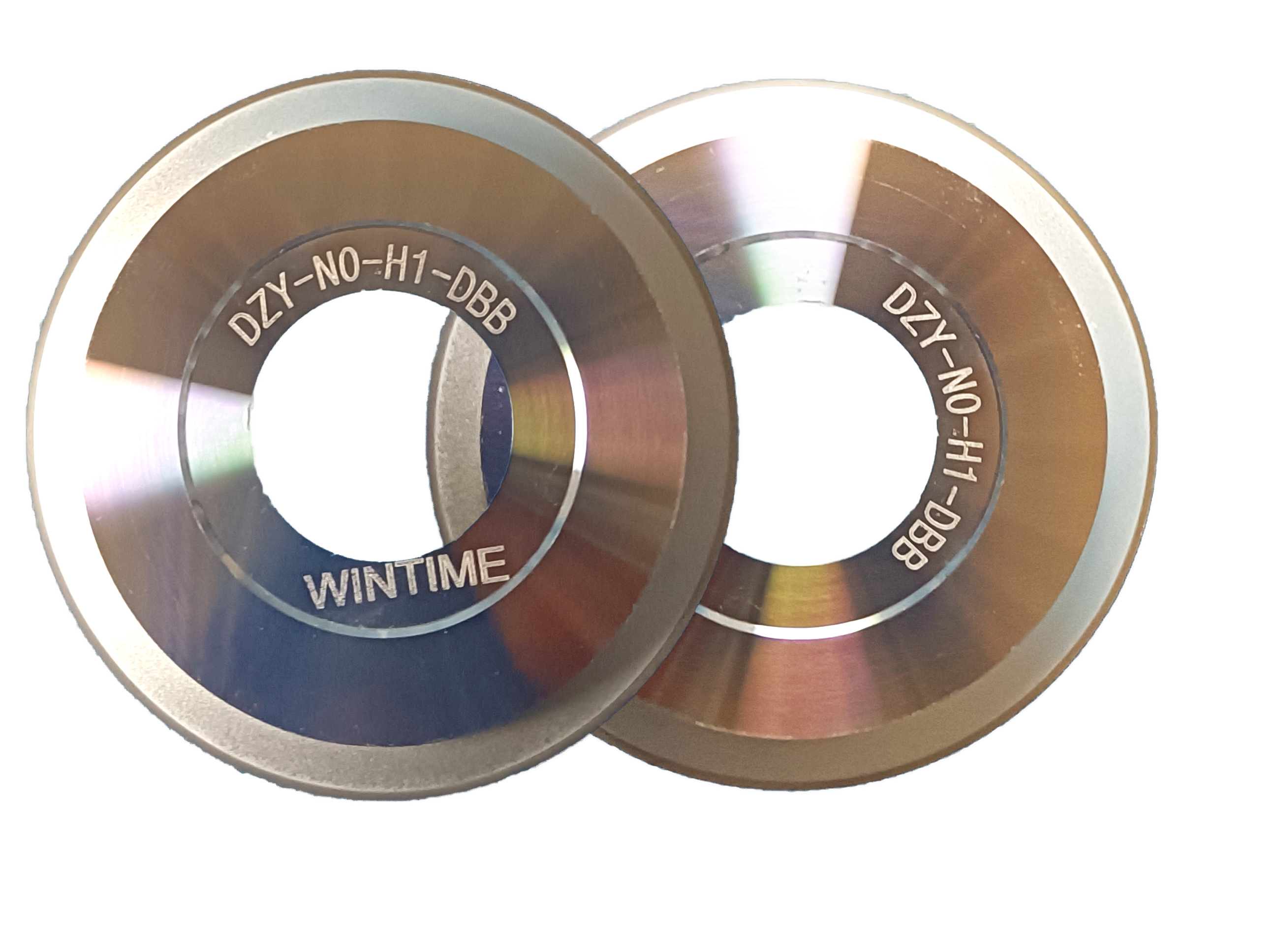
A precision sawing blade is a composite: diamond superabrasive grains held in a bond matrix, on a high-strength steel base where the design includes one. The bond matrix can be resin or metal. The bond is what determines when worn grains are released and fresh grains are exposed — the self-sharpening behaviour that keeps a blade cutting rather than rubbing. A bond that is too hard glazes; a bond that is too soft wears the blade away faster than it wears the workpiece.
WINTIME specifies its sawing blade range with a bond matrix of resin or metal, diamond superabrasive as the working material, and a high-strength steel base where applicable, with blade hardness in the HRC 65–70 range.
Blade construction: hubbed, hubless, flanged, and slotted
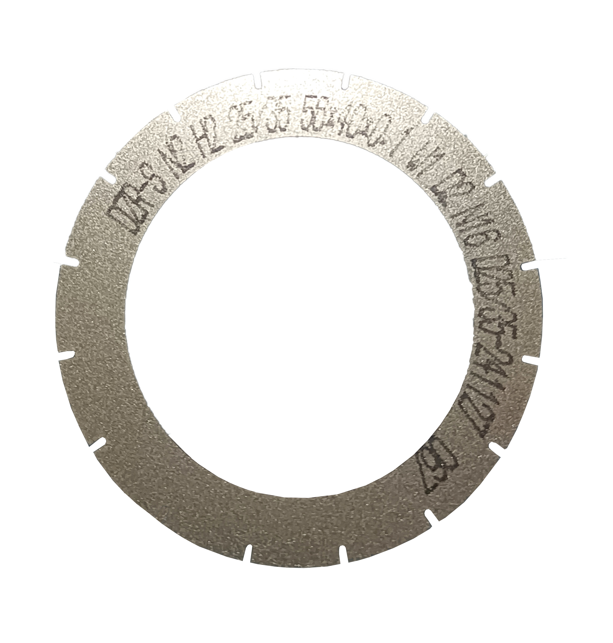
Construction decides how the blade interfaces with the spindle, and interface errors translate directly into runout. The product families used in precision wafer work include diamond sawing blades, precision sawing blades, semiconductor sawing blades, circular sawing blades, hubbed sawing blades, hubless sawing blades, flanged sawing blades, serrated sawing blades, DZY Series wafer sawing blades, DZR Series sawing blades, and DZR-S Series slotted sawing blades.
For ultra-thin work, the hubbed versus hubless choice is the one that most often decides success. A hubbed blade carries an integral hub that gives it a stiffer mounting interface. A hubless blade is a ring without a hub, which lets the cutting edge sit closer to the spindle face and reduces the mass that has to be dynamically balanced — the reason hubless geometry is increasingly dominant for 300 mm processing and substrates below 50 µm.
Dry cutting versus wet cutting
The two operating modes solve the same problem — heat and chip removal — in different ways.
Wet cutting uses a coolant stream directed at the cut. The fluid carries heat away from the bond and flushes kerf debris out of the channel before it can be re-ground, which usually produces the more stable result on brittle or thermally sensitive workpieces. Dry cutting removes the fluid from the process, which is preferred where coolant introduces contamination risk, where post-cut cleaning is a bottleneck, or where the workpiece or tape system is incompatible with liquid. Dry cutting places more of the chip-evacuation burden on blade design, air flow, and feed-rate discipline, and it typically narrows the window in which a given bond formulation performs well.
Both modes are used in production with automatic dicing machines running continuously, and both depend on precision feeding to keep the load per grain predictable.
Precision feeding and spindle dynamics
Feed rate sets how much material each diamond grain has to remove per revolution. Push it too high and the load exceeds what the bond can hold, which shows up as chipping, bond pull-out, or spindle load spikes. Push it too low and the blade rubs instead of cutting, generating heat without removing material.
The operating envelope for WINTIME sawing blades is a spindle speed of 30,000–60,000 rpm, a cutting accuracy of ±0.002 mm, a thickness range of 8 µm to 50 µm, and a chip removal rate of at least 1.2 mm³/s. Those figures describe the machine-side envelope the blade is designed to operate within — they are not automatic outcomes, and they require the cleanroom and support equipment described below.
Why the cleanroom itself is a process parameter
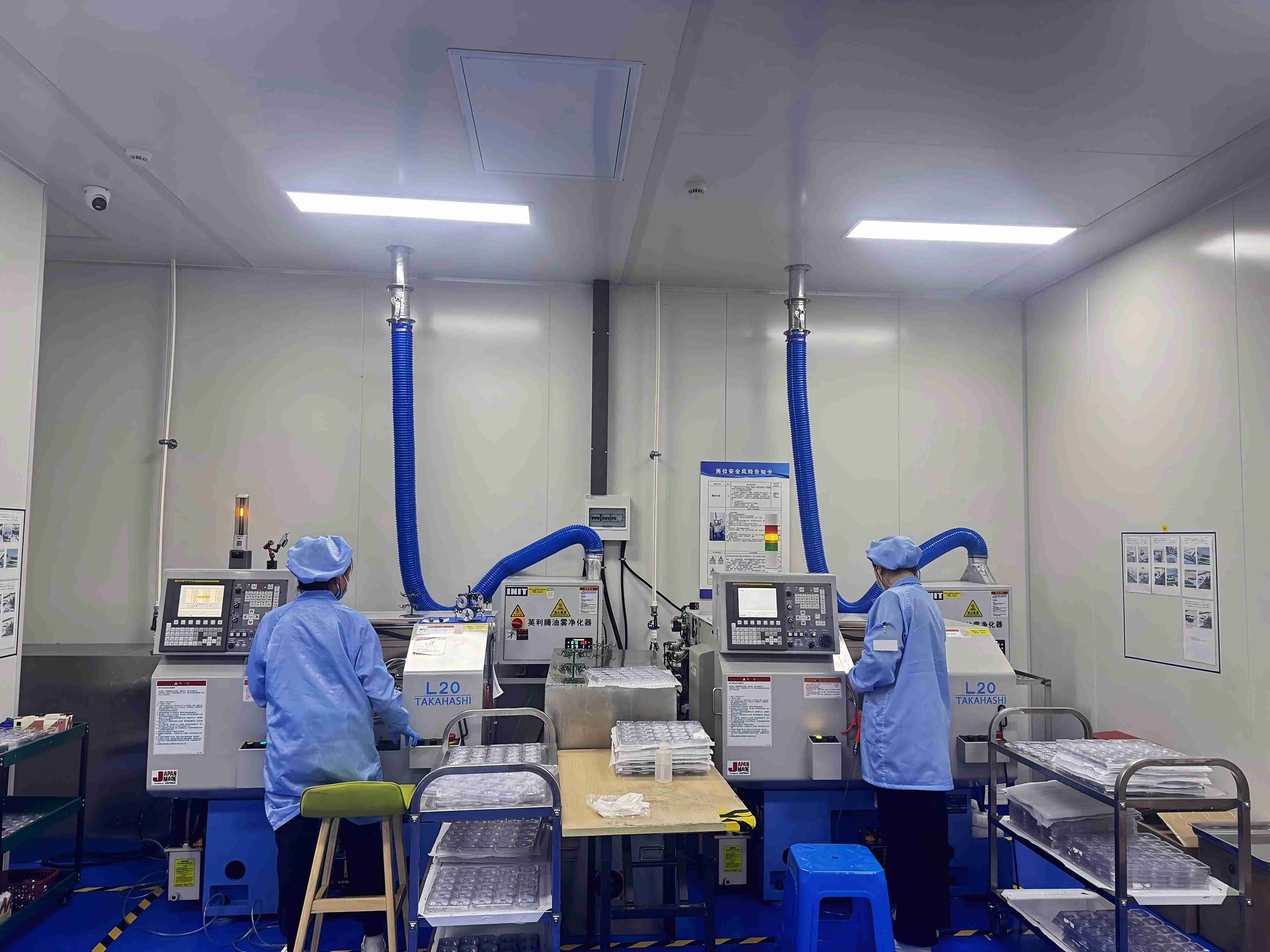
Ultra-thin wafer processing is carried out in a Class 100/1000 cleanroom with constant temperature of 22±2 °C, constant humidity of 45%–55%, and dust-free, anti-static conditions, on machines running high-speed spindles. Each of those conditions is functional rather than cosmetic:
- Class 100/1000 filtration keeps airborne particles from landing in an open kerf whose width is measured in microns.
- 22±2 °C limits thermal expansion of blade, workpiece, and machine structure between measurement and cut.
- 45%–55% relative humidity keeps both electrostatic build-up and condensation risk within bounds.
- Anti-static control prevents charged surfaces from attracting kerf debris and damaging sensitive devices.
Blade specifications for this environment also call for ultra-thin thickness of 9 µm or below, high wear resistance, low cutting loss, anti-static behaviour, high dimensional accuracy, long service life, and stable mass production.
Step-by-Step: A Cleanroom Slicing Sequence
The sequence below is the working order for wafer dicing and scribing, semiconductor package cutting, and comparable precision cuts. Each step constrains the next, so skipping or compressing one usually shows up as chipping or dimensional drift later.
- Establish the cleanroom state. Confirm Class 100/1000 filtration, 22±2 °C, 45%–55% relative humidity, dust-free conditions, and anti-static measures before any wafer is exposed.
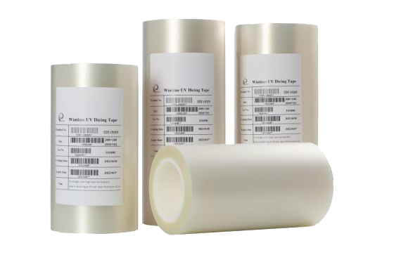
- Mount the workpiece on tape. The wafer or substrate is fixed to UV tape using a UV tape mounting machine. The tape holds the individual die in place during and after cutting and provides mechanical support for thin workpieces.
- Inspect the blade and mount it on the spindle. Verify blade thickness, diameter, and spindle hole dimensions against the specification you are running, then mount on the semiconductor cutting spindle. Dynamic balance is checked at this stage.
- Dress and verify runout. Blade exposure and runout are established before production. Dynamic balance detection with a high-speed dynamic balance tester is part of WINTIME’s own quality control for this reason.
- Align to the street and set the kerf plan. Alignment defines where the cut will be; the kerf plan defines how much material will be lost. Cutting accuracy of ±0.002 mm is the tolerance target on the blade side.
- Cut with precision feeding. The automatic wafer dicing machine advances the workpiece through the blade at a controlled rate while the spindle runs at 30,000–60,000 rpm. Dry or wet cutting is selected according to the material and contamination requirements.
- Manage chips and heat continuously. Coolant flow or dry-mode extraction has to keep up with a chip removal rate of at least 1.2 mm³/s. Chip packing is the most common cause of sudden blade load spikes.
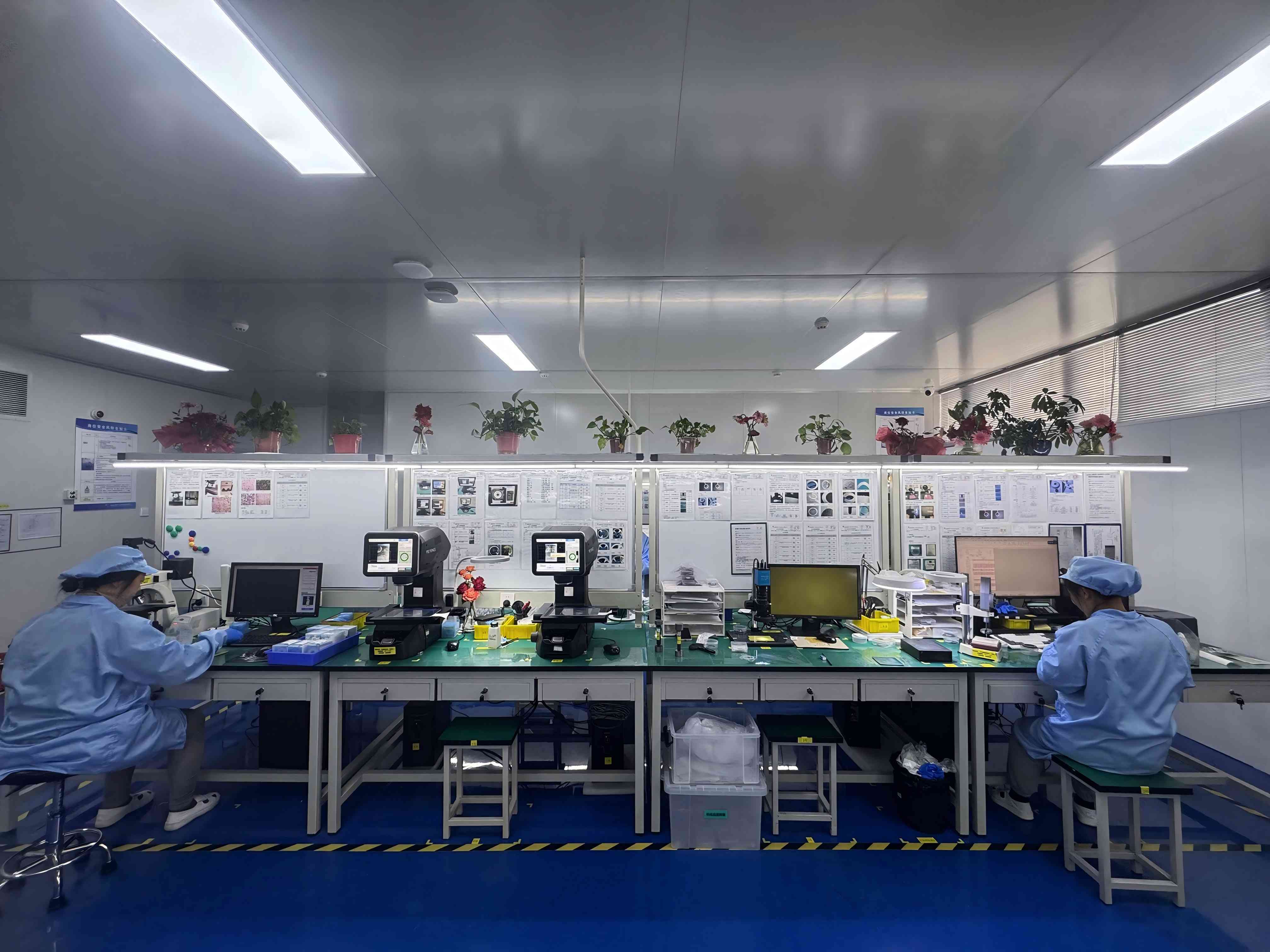
- Clean the workpiece. Wafer cleaning equipment removes kerf debris, coolant residue, and tape residue before the workpiece is handled further.
- Test and inspect. A wafer testing machine verifies die integrity while dimensional checks confirm kerf width and position. UV tape is then cured and the die separated.
Required support equipment
| Equipment | Role in the ultra-thin slicing sequence |
|---|---|
| Automatic wafer dicing machine | Continuous operation and precision feeding of the workpiece through the blade. |
| Semiconductor cutting spindle | Rotates the sawing blade at 30,000–60,000 rpm inside a high-speed spindle environment. |
| UV tape mounting machine | Fixes the wafer on UV tape for support during cutting and for die retention afterwards. |
| Wafer cleaning equipment | Removes kerf debris, coolant, and tape residue after cutting. |
| Wafer testing machine | Verifies die integrity and dimensional results after dicing. |
Use Cases: Where Ultra-Thin Wafer Slicing Applies
The same mechanism serves several workpiece families, each of which shifts the balance between bond type, grain size, and feed parameters.
- Semiconductor wafer dicing and scribing. The core application for a semiconductor wafer sawing blade, including ultra-thin wafer processing where blade thickness of 9 µm or below is required.
- Semiconductor packaging cutting. Cutting of packaged and semi-packaged components, where the priority is dimensional repeatability across long continuous runs.
- Optical communication devices. Optical communication sawing blades serve optical device cutting, a segment that accounted for 16% of the 2024 dicing blade market share driven by 5G infrastructure expansion.
- Functional ceramics and substrates. Functional ceramic sawing blades cut ceramic substrates, where brittleness makes chipping control the deciding criterion.
- Alloy materials. Alloy material sawing blades serve precision alloy component cutting, where metal bond grades are commonly used because of the hardness involved.
- New functional materials. Emerging substrate and device materials that fall outside the established semiconductor and ceramic categories.
Comparing Sawing Blade Options on Verifiable Criteria
Two comparisons drive most specification decisions in ultra-thin work: which bond family to start with, and whether to run hubbed or hubless geometry.
| Criterion | Resin bond sawing blade | Metal bond sawing blade |
|---|---|---|
| Bond matrix | Resin bond | Metal bond |
| Global share of the dicing blade market, 2024 | 42% | 33% |
| Documented material association | Broadly deployed across semiconductor dicing and precision cutting work | Used for harder materials such as SiC |
| WINTIME construction reference | Resin-bond blade construction in the sawing blade range | Metal-bond blade construction in the sawing blade range |
Bond share figures: market.us, Dicing Blade Market Report 2026 (2024 data, global).
| Criterion | Hubbed sawing blade | Hubless sawing blade |
|---|---|---|
| Construction | Blade supplied with an integral hub | Ring blade supplied without a hub |
| Mounting interface | Hub-to-spindle interface | Blade bore to spindle face |
| Stability and runout on thin work | Not the geometry cited in the documented thin-substrate trend | Increasingly dominant for 300 mm wafer processing due to superior stability and reduced runout on substrates below 50 µm |
| Selection logic | Consider where hub-based mounting matches the existing machine interface | Consider where the workpiece is thin and runout is the dominant risk |
How to read these tables. Bond share and hubless adoption are market-level observations, not performance guarantees for a specific machine. The correct order of operations is to fix the workpiece material, the required kerf, and the maximum acceptable chipping level first, then select the bond and geometry that can hold those limits on your spindle.
FAQ
What cleanroom conditions and standards does ultra-thin wafer slicing require?
Ultra-thin wafer processing is carried out in a Class 100/1000 cleanroom with constant temperature of 22±2 °C, constant humidity of 45%–55%, dust-free and anti-static conditions, and a high-speed spindle environment. These conditions are functional: at sub-9 µm kerf widths, airborne particles and static charge are the same size order as the cut itself. On the tool side, diamond tools including sawing blades are categorised under ISO 22180:2019, which distinguishes CVD diamond-coated types from monocrystalline and polycrystalline types.
Can a sawing blade actually cut with a blade thinner than 9 µm?
Yes, and the capability is measurable rather than aspirational. WINTIME Semiconductor Technology Co., Ltd., a Jiangsu-based manufacturer founded in 2020, completed an “Ultra-thin Wafer D Blade” project that achieved a blade thickness below 9 microns, and the company is one of the few domestic manufacturers able to mass-produce at that thickness. The wider product range is specified at a thickness range of 8 µm to 50 µm, cutting accuracy of ±0.002 mm, spindle speed of 30,000–60,000 rpm, and a chip removal rate of at least 1.2 mm³/s. Production backing includes a 34,000 ㎡ facility, an annual output capacity of more than 1 million pieces of dicing blades, and a 35-engineer R&D team.
What drives the cost of an ultra-thin sawing blade?
Public list pricing is not the right frame for this category; the cost drivers are specification and order structure. The variables that materially affect unit cost are blade diameter, thickness and spindle hole size; bond type (resin or metal); diamond abrasive grain size and concentration; coating options such as anti-rust, heat-dissipation or wear-resistant coatings; the cutting performance target for speed and service life; export and special packaging; and whether special-shaped, non-standard geometry is required. Order structure matters as well: the minimum order quantity is 50 pieces for standard products and 300 pieces for customised products, with flexibility for long-term cooperative customers.
How should a buyer validate a blade before committing to mass production?
Validation starts with a standard-specification run rather than a custom tool, because the standard line can be supplied in small quantities — MOQ of 50 pieces — and short lead time. Ask the supplier what quality control the blade has passed. At WINTIME that control includes geometric dimension inspection with vernier caliper and laser diameter gauge, hardness and wear resistance testing on a material testing machine, dynamic balance detection with a high-speed dynamic balance tester, and cutting performance simulation testing against actual material. New customers can also request product application training, and quality problems are investigated with a solution delivered within 48 hours.
What are the lead times and monthly capacity for standard and customised blades?
Standard products ship in 2–5 working days. Customised orders take 10–25 working days, adjustable for large orders. Monthly capacity is more than 800,000 pieces for standard specifications and more than 80,000 pieces for customised and special-shaped products. If you are planning a qualification run or a volume programme, the fastest route is to send the workpiece material, required kerf, target chipping limit, and machine interface to WINTIME and request a quotation and sample specification for your process.
Conclusion: The Blade Is One Component of a Controlled Process
Ultra-thin wafer slicing works because a diamond-bearing blade 8–50 µm thick, rotating at 30,000–60,000 rpm and fed with precision into the workpiece, removes material grain by grain at a controlled rate inside a Class 100/1000 cleanroom held at 22±2 °C and 45%–55% relative humidity. Narrow kerf, low chipping, and stable dimensional control emerge from that combination — blade construction and bond on one side, spindle, UV tape, cleaning, testing, and environment on the other.
For buyers moving from research into evaluation, the practical checklist is short: confirm the cleanroom and support equipment can hold spec, fix the required kerf and chipping limits, decide between hubbed and hubless geometry for your workpiece thickness, choose resin or metal bond against the material being cut, and validate the choice with a measurable cutting performance simulation test before scaling.
Next Step: Specification Review and Sample Request
WINTIME Semiconductor Technology Co., Ltd. manufactures sawing blades and dicing blades for semiconductor manufacturing, semiconductor packaging, optical communication, functional ceramics, and alloy material cutting, with OEM, ODM and customised production available.
Share your workpiece material, target kerf, blade thickness, spindle interface, and required lead time, and the team will respond with a matched specification. Technical support covers cutting process matching and equipment adaptation, with a 35-engineer R&D team and monthly capacity of more than 800,000 pieces behind volume programmes.
Email: shenxiangfei@ntwintime.com | Tel: +86 13851530812 | WhatsApp: +86 18888053207
Address: No. 868, Fushou East Road, Rugao City, Jiangsu Province | Website: en.wintime.net.cn
Download the WINTIME product brochure (PDF) for the full sawing blade and dicing blade range.