
Sawing Blade Options for Optical Device Cutting: A Side-by-Side Buyer Comparison
Sawing Blade options for optical device cutting are usually narrowed by three specifications before price is discussed at all: kerf width, chipping tolerance, and anti-static capability. In optical communication and optoelectronic device production, those three parameters decide how much usable die comes off a wafer, so the comparison has to be run on equal footing. WINTIME Semiconductor Technology Co., Ltd., a manufacturer established in 2020 that specializes in the research, development, production and sales of high-precision cutting blades, documents its SB-001 Sawing Blade platform across a thickness range of 8 μm to 50 μm, a cutting accuracy of ±0.002 mm, and a resin or metal bond choice. This comparison puts the main Sawing Blade options side by side and shows which data points a buyer should demand from every supplier before qualifying a blade.
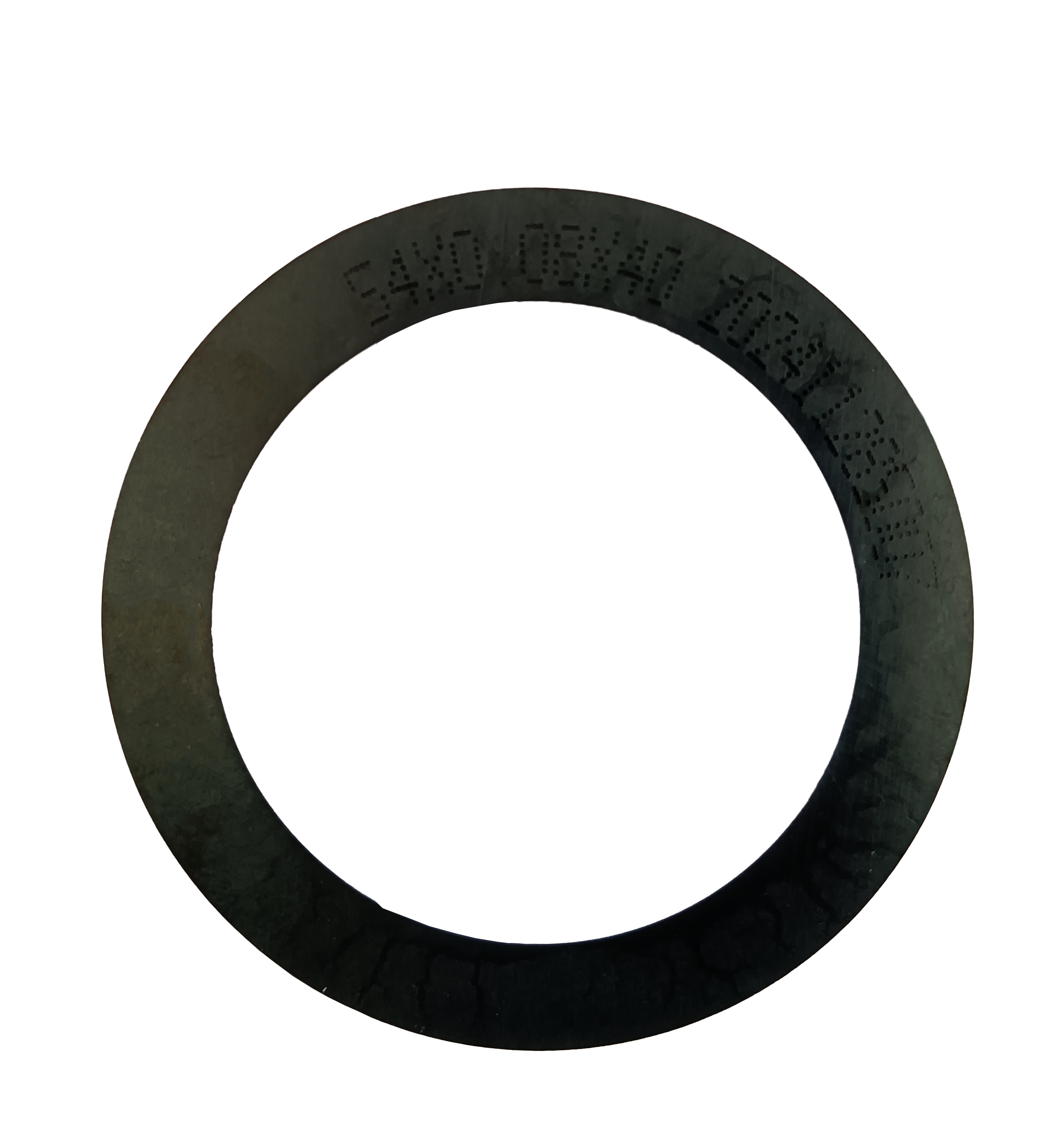
Resin bond blade option - one of the two documented bond routes for the SB-001 Sawing Blade platform.
Problem Definition: Why Optical Cutting Blade Comparisons Go Wrong
Blade data sheets are not written to a shared template. One supplier publishes blade thickness, another publishes kerf. One expresses chipping as a visual acceptance standard, another as a dimensional tolerance. Anti-static is sometimes presented as a property of the blade and sometimes as a condition of the room the blade runs in. The practical result is that buyers end up comparing values that do not describe the same physical thing.
Three friction points repeat in optical device cutting projects:
- Kerf width is quoted as an absolute number. Kerf is not a fixed property of a blade; it is the result of blade thickness plus machine-side behaviour such as runout and feed control. A kerf figure is only comparable when the blade thickness, spindle speed and feed conditions behind it are stated.
- Chipping tolerance has no shared measurement method. Without an agreed inspection method and acceptance window, “low chipping” cannot be verified by either side.
- Anti-static is treated as a blade feature when it is largely an environment requirement. The cutting environment matters as much as the consumable. For this application WINTIME documents a Class 100/1000 clean room, constant temperature of 22±2 °C, constant humidity of 45%–55%, and dust-free, anti-static conditions with high-speed spindles.
In optical device cutting the cost of that mismatch is structural rather than incidental: material removed by the kerf cannot be recovered, and a chipped optical die is scrap. A comparison framework is therefore less about picking a winner and more about forcing every option onto the same measurement basis.
Industry Background: How Large the Optical Cutting Segment Is
Optical device cutting sits inside a large and still growing consumable market, which is why the number of available Sawing Blade options keeps expanding. The global diamond saw blade market was valued at approximately USD 8.60 billion in 2025 and is projected to reach USD 10.16 billion by 2032, according to Maximize Market Research. The narrower wafer dicing blade market was valued at USD 1.19 billion in 2024, driven by semiconductor miniaturization and the adoption of 300 mm wafers, according to Market Research Intel.
Two context points matter for buyers reading those figures. First, published estimates diverge because sources scope the market differently — equipment versus consumables, or full dicing systems versus blades alone. Where different published sources place the same 2024 dicing blade market between roughly USD 0.437 billion and USD 1.31 billion, the honest conclusion is that any single figure is indicative rather than precise. Second, the application mix is shifting: optical communication and RF/optoelectronics applications accounted for 16% of dicing blade market share in 2024, an estimated USD 69.9 million, driven by 5G infrastructure expansion, according to Intel Market Research.
On the technology side, hubless dicing blades are increasingly dominant for 300 mm wafer processing because of superior stability and reduced runout on substrates thinner than 50 µm, according to Semiconductor Equipment Market Data. Bond mix is also split: resin bond blades held a 42% share of the dicing blade market in 2024, while metal bond blades — used for harder materials such as SiC — accounted for 33%, according to a 2026 dicing blade market report published by market.us.
Trade flows reinforce the sourcing reality. China’s exports of cutting blades to Vietnam, India and South Korea grew significantly between 2024 and 2025, with Vietnam increasing by USD 18 million and India by USD 12 million, according to the Observatory of Economic Complexity. For optical device manufacturers, that means a deeper supplier field to compare — and a greater need for a consistent comparison structure.
The Three Comparison Axes to Rank First
1. Kerf Width: Start From Blade Thickness
Kerf width is the material the blade removes on each pass, and it is set primarily by blade thickness. For optical device cutting, where device pitch is tight, the thickness range is the first hard filter. The SB-001 Sawing Blade is documented with a thickness range of 8 µm to 50 µm and a cutting accuracy of ±0.002 mm, and its documented cutting function includes narrow kerf and stable dimensional control.
When a supplier publishes a kerf figure, ask whether it was measured at the same blade thickness, spindle speed and feed rate as your process. The SB-001 platform is documented to run with spindle speeds of 30,000 to 60,000 rpm, which is the range a kerf comparison should reference.
2. Chipping Tolerance: Define the Window Before the Trial
Chipping tolerance is an acceptance criterion, not a catalogue value. The correct sequence is to define the inspection method and the pass/fail window first, then ask each supplier to run against it. The SB-001 Sawing Blade is documented as supporting low chipping as part of its cutting function, and the blade is constructed from a resin or metal bond matrix with diamond superabrasive on a high-strength steel base — the two material variables that most directly influence edge behaviour.
Because chipping is judged on your device, the comparison question to put to every supplier is the same: what chipping result did the blade deliver, on which material, at which feed and spindle speed, and measured how?
3. Anti-Static: Separate the Blade Specification From the Room Specification
Anti-static requirements in optical device cutting belong to two categories that are often conflated. The first is environmental: the SB-001 Sawing Blade application data specifies a Class 100/1000 clean room, a constant temperature of 22±2 °C, a constant humidity of 45%–55%, and a dust-free, anti-static environment with high-speed spindles. The second is the consumable itself, where anti-static performance is documented as part of the special requirement set for ultra-thin cutting, alongside high wear resistance, low cutting loss and long service life.
Buyers should keep the two apart in the comparison table. A supplier that meets the blade requirement but whose process is run outside the specified cleanroom and humidity window is not a comparable data point.
The Sawing Blade Option Landscape: Bond, Hub and Series
The SB-001 is a Sawing Blade categorized as a Diamond Sawing Blade, Precision Sawing Blade, Semiconductor Sawing Blade, Circular Sawing Blade, Hubbed Sawing Blade, Hubless Sawing Blade, Flanged Sawing Blade and Serrated Sawing Blade, and it is offered across named series including the DZY Series Wafer Sawing Blade, the DZR Series Sawing Blade and the DZR-S Series Slotted Sawing Blade. Those three layers — bond, hub configuration and series form factor — are where most side-by-side comparisons actually happen.
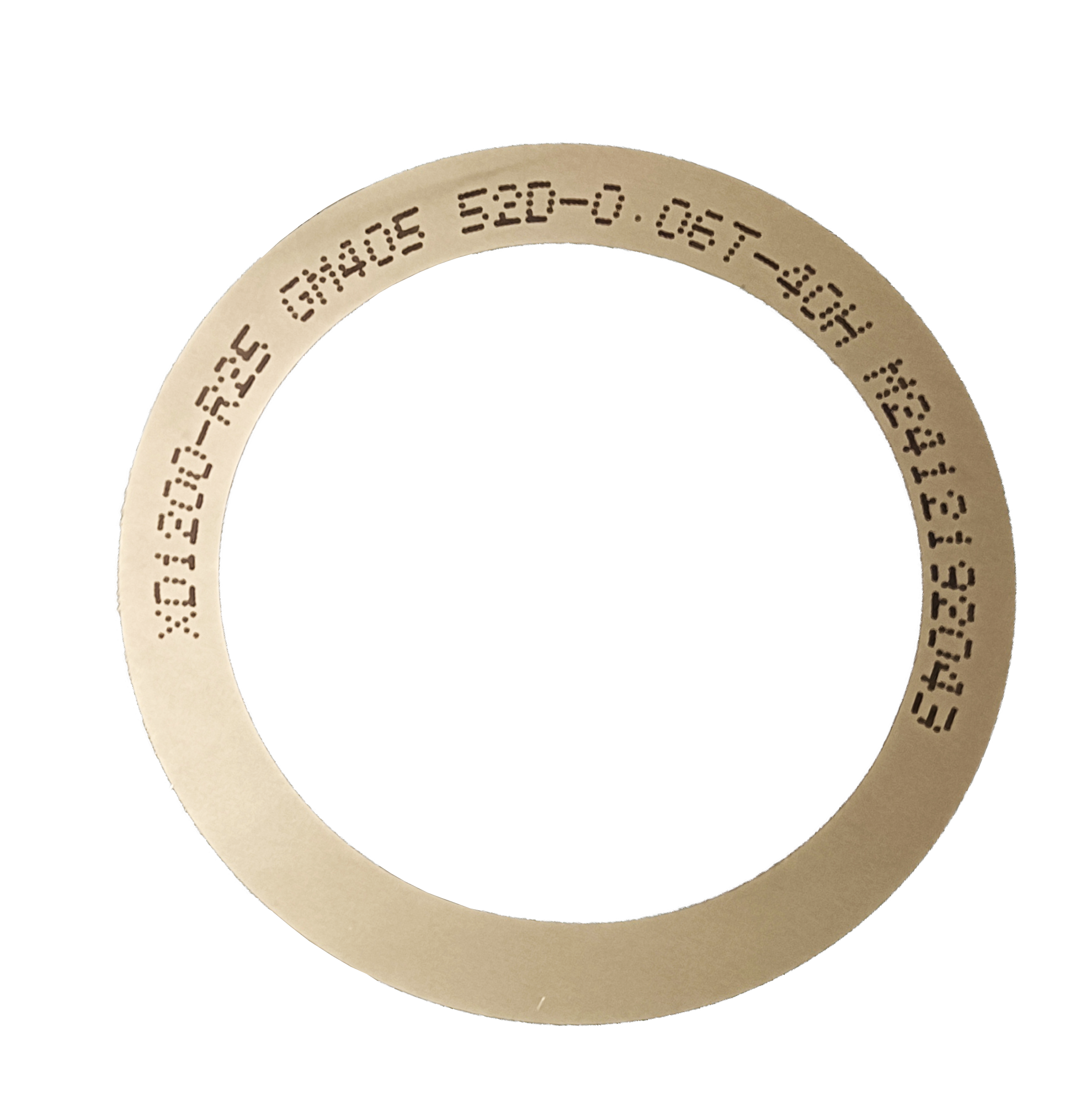
Metal bond option - documented as one of the two bond routes available on the SB-001 Sawing Blade.
Bond route: resin versus metal
The SB-001 Sawing Blade uses resin or metal as its primary bond materials. That split mirrors the wider market, where resin bond blades held 42% of the 2024 dicing blade market and metal bond blades 33%, with metal bond associated with harder materials such as SiC. As general industry practice, resin bonds are commonly selected where a more compliant cutting action is preferred on brittle or thin materials, while metal bonds are commonly selected for harder substrates and longer wear cycles. Because the SB-001 platform supports both, the bond decision can be made on material and device requirements rather than on supplier availability.
Hub configuration: hubless, hubbed and flanged
Hubless, hubbed and flanged configurations are all listed among the SB-001 Sawing Blade categories. The choice is increasingly consequential: hubless dicing blades are becoming dominant for 300 mm wafer processing because of superior stability and reduced runout on substrates thinner than 50 µm, according to Semiconductor Equipment Market Data. Buyers running thin optical substrates should therefore ask what stability evidence exists for the exact hub configuration quoted, rather than for the blade family as a whole.
Series form factor: DZY, DZR and DZR-S
The DZY Series Wafer Sawing Blade, DZR Series Sawing Blade and DZR-S Series Slotted Sawing Blade describe different form-factor and slotting options within the same documented platform. They share the platform specification set, so a buyer comparing them should compare them on the parameters that are actually differentiated: thickness option within the 8 µm to 50 µm range, bond route, hub configuration, and slot geometry.
Terminology note for buyers: electroforming hard sawing blades are also encountered in supplier catalogs, where the abrasive layer is deposited rather than pressed and sintered. WINTIME’s SB-001 Sawing Blade documents resin and metal as its bond materials, so a cross-supplier comparison should be run on the bond route each supplier actually quotes, not on category labels alone.
Documented SB-001 Sawing Blade Specifications
Answer first: the comparable specification set for this platform is a thickness range of 8 µm to 50 µm, cutting accuracy of ±0.002 mm, spindle speed range of 30,000 to 60,000 rpm, hardness of HRC 65–70, a resin/metal bond type, and a chip removal rate of ≥1.2 mm³/s. These values apply to the SB-001 Sawing Blade platform and should be requested in the same format from any alternative supplier.
| Parameter | Documented value | Why it belongs in the comparison |
|---|---|---|
| Thickness range | 8 µm – 50 µm | Sets the material removed per cut and the feasibility of ultra-thin slicing |
| Cutting accuracy | ±0.002 mm | Dimensional control target for small optical devices |
| Spindle speed | 30,000 – 60,000 rpm | Machine-side compatibility window |
| Hardness | HRC 65–70 | Hardness band of the blade platform |
| Bond type | Resin / metal | Primary selection axis for material and wear behaviour |
| Chip removal rate | ≥1.2 mm³/s | Debris evacuation and throughput reference |
| Construction | Resin or metal bond matrix, diamond superabrasive abrasive, high-strength steel base | Explains where the wear and stability characteristics come from |
| Intended industries | Semiconductor manufacturing, semiconductor packaging, precision electronic component processing, optical ceramic cutting | Confirms scope fit for optical device cutting |
Step-by-Step Breakdown: A Seven-Step Comparison Workflow
- Define the cut, not the blade. Record the device type, material stack, target thickness and required dimensional tolerance. In optical device cutting this usually means stating the finished device dimension and the acceptable material loss per pass.
- Convert the loss budget into a blade thickness target. Filter options against the 8 µm to 50 µm documented range and discard any option that cannot be quoted inside your window.
- Select the bond route. Choose resin or metal against your material hardness and wear cycle. Resin bond accounted for 42% and metal bond 33% of the 2024 dicing blade market, so both routes are mainstream; the SB-001 platform documents both.
- Select the hub configuration. Hubless, hubbed and flanged options are all available on this platform. For substrates below 50 µm, weight the stability and runout evidence that hubless designs are reported to offer for 300 mm processing.
- Set the chipping acceptance window in writing. Agree the inspection method and the pass/fail limit before any trial cut, then require every supplier to report against that same standard.
- Confirm the environment specification. Verify the Class 100/1000 clean room, 22±2 °C, 45%–55% relative humidity and anti-static conditions that the SB-001 application data specifies, and confirm which of these are blade-side and which are room-side.
- Confirm equipment and consumable fit. The platform is documented to require an automatic wafer dicing machine, semiconductor cutting spindle, UV tape mounting machine, wafer cleaning equipment and wafer testing machine, and to run in high-speed spindle rotating mode with dry/wet cutting and precision feeding. An option that does not fit this equipment set is not a real alternative.
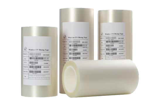
Supporting consumable: UV film is listed among the equipment and consumables that this cutting process depends on.
Use Cases: Where the Options Land
Optical communication and optoelectronic device cutting
Optical communication and RF/optoelectronics represented 16% of dicing blade market share in 2024, an estimated USD 69.9 million, according to Intel Market Research. The SB-001 Sawing Blade is documented as suitable for optical device cutting and for use in optical ceramic cutting, with the application scenario common in China, Japan, Korea, Singapore, Malaysia, the United States and Germany.
Ultra-thin wafer processing
The documented special requirement for this application set includes ultra-thin blade thickness of ≤9 µm, high wear resistance, low cutting loss, anti-static performance, high dimensional accuracy and stable mass production. WINTIME’s “Ultra-thin Wafer D Blade” project has achieved a process thickness of less than 9 microns.
Ceramic substrate and functional ceramic cutting
The same platform is documented as suitable for ceramic substrate cutting and is used in the functional ceramics and new functional materials industries — a useful reference point when an optical device program also carries ceramic components.
Precision alloy component cutting
Precision alloy component cutting is listed among the suitable projects, extending the comparison beyond wafer work to alloy materials where bond choice and wear resistance dominate.
Comparison Table: Sawing Blade Options Side by Side
| Option | Documented data point | Primary selection signal | Must be verified before order |
|---|---|---|---|
| Resin bond sawing blade | Listed as a primary bond material for the SB-001 Sawing Blade; resin bond held 42% of the 2024 dicing blade market | Brittle or thin optical material where a more compliant bond action is preferred | Chipping result on your material; thickness option within 8–50 µm |
| Metal bond sawing blade | Listed as a primary bond material for SB-001; metal bond held 33% of the 2024 market, used for harder materials such as SiC | Harder substrates and longer wear cycles | Wear behaviour over a defined cut count; kerf consistency |
| Hubless sawing blade | Listed among SB-001 categories; hubless designs are increasingly dominant in 300 mm wafer processing for stability and reduced runout below 50 µm | Thin substrates where runout directly affects kerf and chipping | Stability evidence for the exact quoted configuration |
| Hubbed / flanged sawing blade | Both configurations are listed among SB-001 categories | Processes with existing spindle and flange tooling | Flange fit, mounting procedure and accuracy after mounting |
| DZY Series wafer sawing blade | Listed series on the SB-001 platform; shares the documented 8–50 µm thickness range and ±0.002 mm accuracy | Wafer dicing and scribing, including ultra-thin work | Thickness option, bond route and hub configuration actually quoted |
| DZR Series sawing blade | Listed series on the same platform and specification set | General precision cutting within the semiconductor stack | Same specification confirmation; chipping acceptance method |
| DZR-S Series slotted sawing blade | Listed slotted series on the same platform and specification set | Processes requiring a slotted form factor rather than a plain circular edge | Slot geometry fit against the device layout |
| Diamond / circular / serrated sawing blade | All listed among SB-001 product categories; construction is diamond superabrasive on a high-strength steel base | Selection follows the cut geometry rather than brand preference | Confirmation that the category matches the intended cut |
Read the table as a filter, not a ranking. The correct option is the one whose documented values survive all four columns — and no option should progress to volume use without passing the chipping and kerf checks on your own device.
Supplier-Side Checks Before You Commit
Answer first: blade specifications only hold if the supplier can reproduce them at volume. WINTIME Semiconductor Technology Co., Ltd. operates a manufacturing facility covering 34,000 square meters with approximately 100 staff, a research and development team of 35 engineers, 2 patent technologies, and an annual production capacity of 1 million pieces. The company is one of the few domestic manufacturers capable of mass-producing ultra-thin wafer dicing blades.

Engineering and commercial coordination behind the SB-001 Sawing Blade platform.
Three supplier-side checks belong in any optical device cutting comparison:
- Volume reproducibility. Ask how the 8 µm to 50 µm thickness range and the ±0.002 mm accuracy are controlled in production, not only in a sample.
- Documentation and standards alignment. Diamond tools, including sawing blades, are categorized under ISO 22180:2019, which distinguishes between CVD diamond-coated and monocrystalline/polycrystalline types. Buyers should ask which standard or internal specification a supplier’s documentation references, so that the comparison is against a named framework rather than marketing language.
- Market presence and continuity. Export business accounts for 30% of WINTIME’s total sales, with major markets in Southeast Asia, East Asia, North America and the European Union. In the wider high-precision dicing blade market, named participants published by Credence Research include DISCO Corporation, Tokyo Seimitsu (Accretech), Advanced Dicing Technologies (ADT) and Asahi Diamond — a useful reference set when benchmarking what a qualified supplier profile looks like, without treating any single supplier as a default.
FAQ: Comparing Sawing Blade Options for Optical Device Cutting
Q1. Does an optical device Sawing Blade need cleanroom and anti-static qualification, and how is that documented?
The application environment for this cutting process is documented as a Class 100/1000 clean room with a constant temperature of 22±2 °C, a constant humidity of 45%–55%, and dust-free, anti-static conditions with high-speed spindles. Anti-static performance also appears in the documented special requirement set for ultra-thin cutting, alongside high wear resistance, low cutting loss and long service life. On the documentation side, diamond tools including sawing blades fall under ISO 22180:2019, which distinguishes CVD diamond-coated from monocrystalline/polycrystalline types; buyers should confirm which standard a supplier’s documentation references, and should separate room-side requirements from blade-side requirements when they write the purchase specification.
Q2. Can one Sawing Blade platform cover hubless, metal-bond and slotted requirements for optical work?
The SB-001 Sawing Blade is documented as a Diamond Sawing Blade, Precision Sawing Blade, Semiconductor Sawing Blade, Circular Sawing Blade, Hubbed Sawing Blade, Hubless Sawing Blade, Flanged Sawing Blade and Serrated Sawing Blade, offered across the DZY Series Wafer Sawing Blade, DZR Series Sawing Blade and DZR-S Series Slotted Sawing Blade. Its bond materials are resin or metal, its construction combines a resin or metal bond matrix with diamond superabrasive on a high-strength steel base, and its documented thickness range is 8 µm to 50 µm with cutting accuracy of ±0.002 mm. Hubless designs are increasingly dominant in 300 mm wafer processing for stability and reduced runout below 50 µm, so the specific hub configuration quoted should still be confirmed separately from the platform capability.
Q3. How should buyers compare cost between Sawing Blade options when quotations are structured differently?
Because the options differ in kerf and chipping behaviour, unit price alone is not a comparable number. A workable cost comparison normalises at least five inputs: material lost per cut against the quoted blade thickness, the chipping acceptance result measured on your device, the blade wear cycle, the qualification time required to reach a stable process, and the supporting consumables the process depends on — an automatic wafer dicing machine, semiconductor cutting spindle, UV tape mounting machine, wafer cleaning equipment and wafer testing machine are all documented requirements. Only after those inputs are fixed does price become comparable. Suppliers should be asked to quote against the same thickness window and the same chipping standard, so that differences reflect blade behaviour rather than quotation structure.
Q4. What should a first sample cut prove before an optical cutting blade is released to volume?
A sample cut should verify five things against documented values: that the delivered blade sits inside the quoted thickness range of 8 µm to 50 µm, that cut position holds to ±0.002 mm on your equipment, that the chipping result meets the window agreed in writing, that the blade runs correctly within the 30,000 to 60,000 rpm spindle range, and that handling and mounting in the cleanroom and anti-static environment works in practice. Chipping tolerance and kerf width should be measured the same way on the sample as they will be measured in production. Sample and quotation requests for the SB-001 Sawing Blade can be sent to shenxiangfei@ntwintime.com or via WhatsApp at +8618888053207, with the device type, target thickness and acceptance window included so the correct thickness and bond route can be quoted.
Q5. How can buyers verify supply continuity for a multi-year optical device program?
Supply continuity checks should be answered with verifiable figures rather than statements of intent. WINTIME Semiconductor Technology Co., Ltd. operates a manufacturing facility covering 34,000 square meters with approximately 100 staff, an annual production capacity of 1 million pieces, a research and development team of 35 engineers, and 2 patent technologies; the company is documented as one of the few domestic manufacturers capable of mass-producing ultra-thin wafer dicing blades, and its “Ultra-thin Wafer D Blade” project has achieved a process thickness of less than 9 microns. Export business accounts for 30% of total sales, serving Southeast Asia, East Asia, North America and the European Union. Buyers should ask for the same four categories of evidence from any alternative supplier: capacity, engineering depth, patented or proprietary process assets, and existing export coverage in their region.
Conclusion: Compare on Kerf, Chipping and Anti-Static — Then Verify on Your Device
Sawing Blade options for optical device cutting are comparable only when kerf width is tied to blade thickness, chipping tolerance is tied to an agreed inspection method, and anti-static requirements are split between the blade and the room. Once those three axes are fixed, the remaining decision is a fit question: does the option match your material, your hub and flange tooling, your spindle speed range and your cleanroom conditions.
The SB-001 Sawing Blade platform from WINTIME covers the ground most optical cutting projects need — 8 µm to 50 µm thickness, ±0.002 mm accuracy, resin or metal bond, and hubbed, hubless, flanged, serrated, DZY, DZR and DZR-S configurations on a shared specification set — and it is documented for optical device cutting and optical ceramic cutting within a Class 100/1000, anti-static environment. As with any consumable, the documented values open the shortlist; the sample cut closes it.
Next step: request a sample or quotation
To run a comparison of your own, send the device type, target thickness and chipping acceptance window to WINTIME Semiconductor Technology Co., Ltd. You will receive the matching thickness and bond recommendation for the SB-001 Sawing Blade platform, plus the technical documentation needed to score it against your current blade.
Email: shenxiangfei@ntwintime.com | Tel: +86 13851530812 | WhatsApp: +8618888053207
Website: en.wintime.net.cn
Address: No. 868, Fushou East Road, Rugao City, Jiangsu Province, China
Download the full product brochure: WINTIME Sawing Blade brochure (PDF)
Sample and quotation coordination for Sawing Blade projects.