
Sawing Blade Selection Parameters for Cleanroom Semiconductor Dicing: A Technical Guide
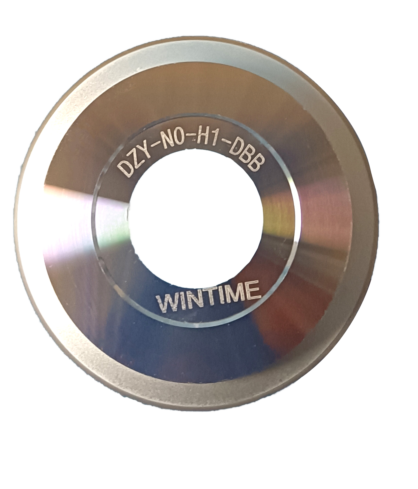
DZY series wafer sawing blade — a hubless-type blade family used for ultra-thin silicon dicing inside Class 100/1000 environments.
Introduction: Six Parameter Clusters Decide the Blade
Choosing a sawing blade for cleanroom semiconductor dicing is a parameter-matching exercise rather than a catalogue pick. Six clusters decide the outcome: blade thickness (down to ≤9 μm on ultra-thin programmes, inside an 8 μm–50 μm production range), bond matrix and abrasive construction, cutting accuracy (±0.002 mm), spindle compatibility (30,000–60,000 rpm), anti-static and cleanroom behaviour (Class 100/1000, 22±2 °C, 45%–55% RH), and the ability to repeat all of the above inside continuous mass production.
These six clusters are treated together because a blade that satisfies five of them can still pass a sample test and fail in volume. A blade selected only for a thin kerf may cut a trial wafer cleanly and then drift once a machine has run for a full shift. A blade with the correct dimensional number on paper may still behave differently inside a dry-cut cleanroom aisle. In cleanroom dicing, the parameters interact; they do not stack independently.
This guide is written for process engineers, packaging line managers and sourcing teams who have moved past the definition stage and now need to decide which specification to lock first. It covers the parameter logic, the equipment chain a blade has to fit into, the application cases where each parameter dominates, and the questions buyers usually raise before sampling. WINTIME Semiconductor Technology Co., Ltd. (WINTIME) — a Jiangsu-based developer and manufacturer of high-precision sawing blades and dicing blades established in 2020 — is used near the end as a worked example of how these parameters translate into production capability.
Problem Definition: Why Cleanroom Dicing Punishes Partial Specification
The problem is not that dicing blades are hard to buy. It is that a dicing line evaluates the blade through three simultaneous channels — geometry, contamination, and repeatability — and a specification that is incomplete in any one of them shows up only after the blade is already installed.
Kerf and material loss. Every micrometre of blade thickness becomes removed material across the whole wafer. Thickness therefore drives yield per wafer before cutting quality is even discussed, which is why ultra-thin wafer programmes treat thickness as the first locked parameter rather than a late-stage refinement.
Chip formation and dimensional drift. Chipping and drift are the two failure modes that most often reach the quality report. Both are produced by the interaction of blade hardness, bond type, feed rate and spindle behaviour — not by blade thickness alone. A blade can be geometrically correct and still generate chipping if the bond releases abrasive at the wrong rate for the substrate.
Static and particulate behaviour. In a dry-cut or low-moisture environment, friction between blade, substrate and debris can produce charge that is unacceptable near sensitive devices. Anti-static behaviour in a cleanroom is a sealing and bonding question as much as a machine question.
Equipment chain fit. A blade also has to fit a hardware chain rather than stand alone. A sawing blade for wafer dicing requires supporting equipment such as an automatic wafer dicing machine, a semiconductor cutting spindle, a UV tape mounting machine, wafer cleaning equipment and a wafer testing machine. Selection therefore begins with the machine, the tape and the cleaning step — not with the blade in isolation.
Industry Background: Where Dicing Blade Demand Stands
The wafer dicing blade market was valued at USD 1.19 billion in 2024, according to Market Research Intel, driven by semiconductor miniaturisation and the adoption of 300 mm wafers. The broader diamond saw blade category that contains precision dicing blades was valued at approximately USD 8.60 billion in 2025 and is expected to reach USD 10.16 billion by 2032, according to Maximize Market Research. Published dicing blade figures differ by scope — some estimates cover equipment, others cover consumables — so any single number should be read as directional rather than exact.
Bond composition is one of the clearest structural signals in the category. In 2024, resin bond blades held a 42% share of the dicing blade market, while metal bond blades — the type used for harder materials such as SiC — accounted for 33%, per the Dicing Blade Market Report 2026. Hubless dicing blades are increasingly dominant for 300 mm wafer processing because of their stability and reduced runout on thinner substrates below 50 µm. Optical communication and RF/optoelectronics applications accounted for 16% of dicing blade market share in 2024, with 5G infrastructure expansion cited as a driver.
Standardisation is relevant to buyers comparing suppliers. Diamond tools, including sawing blades, are categorised under ISO 22180:2019, which distinguishes between CVD diamond-coated and monocrystalline or polycrystalline types. Publicly identified participants in the high-precision semiconductor dicing blade segment include DISCO Corporation, Tokyo Seimitsu (Accretech), Advanced Dicing Technologies (ADT) and Asahi Diamond; they are named here as reference points for benchmarking, not as a ranking.
Detailed Selection Solution: Parameter by Parameter
1. Thickness and Kerf Budget Come First
Thickness is the parameter that determines how much material is surrendered per cut, and it is the hardest parameter to change once a process is qualified. In practice, sawing blades for this application are specified across a thickness range of 8 μm to 50 μm. Ultra-thin programmes push to the low end, where an achieved process thickness of less than 9 μm has been demonstrated on the "Ultra-thin Wafer D Blade" project by WINTIME — a project that has placed the company among the few domestic manufacturers able to mass-produce ultra-thin wafer dicing blades.
The practical rule is to define the kerf budget before defining anything else. Once the maximum acceptable kerf is fixed by yield calculations, the compatible thickness window narrows, and the remaining parameters — bond, hardness, feed — are selected to protect that window. Selecting a bond first and a thickness later usually means re-qualifying the process.
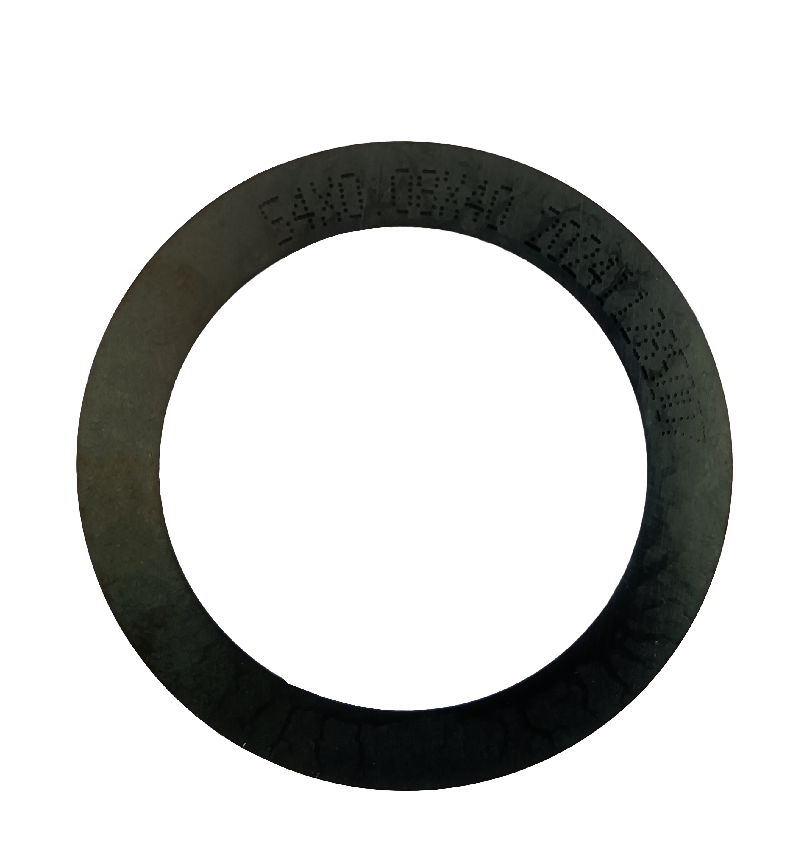
SZ Series resin dicing blade — resin bond is one of the two bond families used in precision dicing blades.
2. Bond Matrix, Abrasive and Blade Body
A precision sawing blade is constructed from a bond matrix of resin or metal, diamond superabrasive as the cutting medium, and a high-strength steel base. The bond type is listed as resin or metal on the SB-001 sawing blade specification, and the same two families dominate the market as a whole: resin bond 42% and metal bond 33% of the 2024 dicing blade market respectively.
The selection question is not which bond is better in general, but which bond matches the substrate hardness and the required surface finish. Metal bond blades are the type used for harder materials such as SiC, which makes bond choice a substrate-driven decision rather than a supplier preference. The steel base deserves the same scrutiny as the abrasive: base stability governs runout, and runout governs the achievable dimensional control regardless of how precise the abrasive layer is.
3. Cutting Accuracy and Dimensional Control
Cutting accuracy is specified at ±0.002 mm on this blade platform. That figure is only meaningful when it holds across a production run, not across a single cut, because die placement, downstream bonding and optical alignment all inherit the positioning error created during dicing.
Three inputs determine whether the stated accuracy is repeatable: blade hardness (HRC 65–70 on this specification), chip removal rate (≥1.2 mm³/s), and the consistency of the feed system. A blade that meets its accuracy target at the start of a run but not at the end has a wear or debris problem, not an accuracy problem. This is why accuracy should always be verified together with wear behaviour rather than separately.
4. Anti-Static Behaviour and Cleanroom Compatibility
Cleanroom conditions are part of the blade specification, not a background assumption. The operating environment for this class of blade is a Class 100/1000 clean room, constant temperature of 22±2 °C, constant humidity of 45%–55%, dust-free and anti-static, combined with a high-speed spindle environment. Each of those values constrains a buying decision.
Humidity at 45%–55% keeps both static build-up and moisture-related contamination inside manageable limits; the anti-static requirement is what protects devices when dry cutting is used. A blade that performs acceptably in an uncontrolled workshop environment can still fail qualification in a Class 100/1000 line, because the failure is environmental rather than mechanical. Buyers should therefore confirm the blade is qualified for continuous operation under exactly these conditions.
5. Wear Resistance and Stable Mass Production
Wear resistance is the parameter that separates a working sample from a working supply. It shows up as blade life, kerf stability over thousands of cuts, and the frequency of blade changes during a shift. High wear resistance, low cutting loss, high dimensional accuracy and long service life are the stated special requirements for this application, and all four are assessed on the same production evidence.
This is where process capability at the supplier matters more than any individual number. A specification can be achieved in a laboratory and lost in manufacturing. Suppliers with mature mass production for ultra-thin blades, a controlled facility and a dedicated engineering team are better positioned to reproduce the same parameter set across batches.
6. Spindle Speed, Cutting Mode and Feed Control
The blade must be matched to the machine before it is matched to the wafer. The compatible spindle speed range for this blade platform is 30,000 to 60,000 rpm, and the cutting mode covers high-speed spindle rotating cutting, both dry and wet cutting, continuous operation on automatic dicing machines, and precision feeding.
Feed behaviour determines whether the intended combination of narrow kerf, low chipping and stable dimensional control is actually reached. In the intended application, the function of the blade is to realise high-precision wafer cutting, ultra-thin slicing, narrow kerf, low chipping, high-efficiency cutting and stable dimensional control. None of those outcomes are produced by the blade alone; they are produced by the blade, spindle, feed profile and cleaning step working inside the same window.
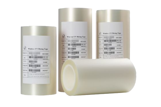
UV tape and the UV tape mounting machine form one link in the equipment chain a dicing blade must fit into.
7. Mapping Parameters to the Product Family
Once the six parameter clusters are fixed, they map onto a blade family rather than a single item. The SB-001 sawing blade platform includes Diamond Sawing Blade, Precision Sawing Blade, Semiconductor Sawing Blade, Circular Sawing Blade, Hubbed Sawing Blade, Hubless Sawing Blade, Flanged Sawing Blade, Serrated Sawing Blade, DZY Series Wafer Sawing Blade, DZR Series Sawing Blade and DZR-S Series Slotted Sawing Blade configurations.
The distinction matters for selection. Hubbed and hubless formats differ in how the blade is supported and whether a flange is required, and the hubless format has become increasingly dominant in 300 mm wafer processing because of its stability on thinner substrates. Slotted and wafer-series formats exist because different die layouts and materials need different edge behaviour. Buyers should treat the family list as a selection map: substrate and format first, then the parameter sheet.
Step-by-Step Breakdown: A Seven-Step Selection Workflow
The sequence below keeps parameter decisions in the order that avoids re-qualification. It is written for a first blade project as well as for a re-specification after a yield or chipping problem.
- Define the project type. Write down which of these you are running: wafer dicing and scribing, semiconductor package cutting, ultra-thin wafer processing, optical device cutting, ceramic substrate cutting, or precision alloy component cutting. The project type sets which parameters dominate.
- Fix the kerf budget. Convert the maximum acceptable material loss into a maximum blade thickness, then locate the thickness inside the 8 μm–50 μm band — or below 9 μm if an ultra-thin programme is required.
- Select the bond and abrasive. Match resin or metal bond to the substrate hardness, using metal bond where harder materials are involved, and confirm the abrasive and steel base construction.
- Confirm accuracy and hardness targets. Record the required cutting accuracy (±0.002 mm on this platform) and the blade hardness class (HRC 65–70) so that the accuracy claim can be verified against wear behaviour.
- Check spindle and feed compatibility. Verify the blade against the machine's spindle speed window (30,000–60,000 rpm), the dry or wet cutting mode, and the feed profile used by the automatic dicing machine.
- Confirm cleanroom and anti-static requirements. Check Class 100/1000 suitability, 22±2 °C and 45%–55% RH operating conditions, and dust-free, anti-static operation with high-speed spindles.
- Validate on samples, then scale. Run the blade through the full equipment chain — dicing machine, semiconductor cutting spindle, UV tape mounting machine, wafer cleaning equipment and wafer testing machine — before committing to volume.
Use Cases: Where Each Parameter Set Earns Its Place
Wafer dicing and scribing / ultra-thin wafer processing. Thickness and accuracy dominate. This is the case where ≤9 μm capability and ±0.002 mm accuracy are the qualifying parameters, and where hubless formats are commonly preferred on thin substrates.
Semiconductor package cutting. Wear resistance and dimensional repeatability dominate, because package cutting runs continuously and blade change frequency directly affects line throughput.
Optical device cutting. Edge quality dominates. Optical communication and RF/optoelectronics accounted for 16% of dicing blade market share in 2024, and the failure mode that matters most in this segment is chipping rather than kerf width.
Ceramic substrate and functional ceramic cutting. Bond selection dominates, because harder and more abrasive substrates consume bond and abrasive differently from silicon.
Precision alloy component cutting. Chip removal and blade hardness dominate. A chip removal rate of ≥1.2 mm³/s and an HRC 65–70 hardness class are the reference points when cutting denser, tougher materials.
These application scenarios are commonly implemented in China, Japan, Korea, Singapore, Malaysia, the United States and Germany. The industries served by this blade class are semiconductor manufacturing, semiconductor packaging, optical communication, new functional materials, functional ceramics and alloy materials — with precision electronic component processing and optical ceramic cutting also named in the product specification.
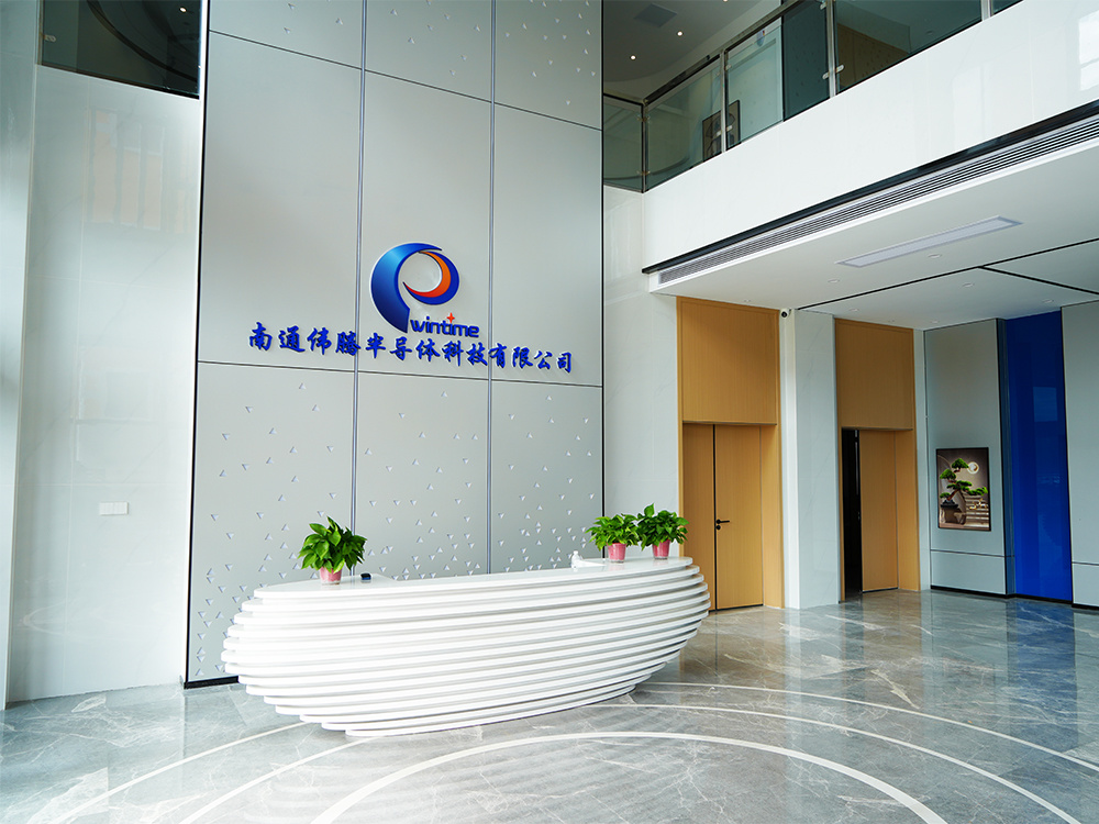
WINTIME operates a 34,000 ㎡ manufacturing facility with about 100 staff, including an R&D team of 35 engineers.
Comparison Table: Verified Parameter Reference
The table below consolidates the measurable parameters that a buyer should request on a single specification sheet before sampling. Every value is taken from the published product and application specification for the SB-001 sawing blade.
| Parameter | Specified value | Why it decides the selection |
|---|---|---|
| Blade thickness range | 8 μm – 50 μm | Sets kerf width and material loss per cut |
| Ultra-thin programme thickness | ≤9 μm (achieved process thickness, "Ultra-thin Wafer D Blade" project) | Determines feasibility of ultra-thin wafer slicing |
| Cutting accuracy | ±0.002 mm | Drives die placement and downstream alignment tolerance |
| Spindle speed range | 30,000 – 60,000 rpm | Confirms compatibility with the dicing spindle |
| Blade hardness | HRC 65–70 | Indicates wear behaviour across long production runs |
| Chip removal rate | ≥1.2 mm³/s | Governs debris clearing in dry and wet cutting |
| Bond type | Resin / metal | Matched to substrate hardness, e.g. metal bond for harder materials such as SiC |
| Construction | Resin or metal bond matrix + diamond superabrasive + high-strength steel base | Base stability governs runout and achievable accuracy |
| Operating environment | Class 100/1000; 22±2 °C; 45%–55% RH; dust-free; anti-static | Qualification condition for cleanroom lines |
| Model designation | SB-001 | Reference used when requesting a quotation |
Frequently Asked Questions
What cleanroom conditions must a sawing blade for semiconductor dicing operate in?
The operating conditions specified for this class of sawing blade are a Class 100/1000 clean room with constant temperature of 22±2 °C, constant humidity of 45%–55%, and a dust-free, anti-static environment used together with high-speed spindles. These conditions are part of the qualification requirement rather than a facility preference: humidity control and anti-static behaviour are what allow the blade to run in dry or wet cutting modes without contaminating or electrically stressing sensitive devices. Diamond tools, including sawing blades, fall under ISO 22180:2019, which distinguishes between CVD diamond-coated and monocrystalline or polycrystalline types.
How thin can an ultra-thin wafer dicing blade be, and what accuracy comes with it?
The SB-001 sawing blade platform is specified across a thickness range of 8 μm to 50 μm, with an achieved process thickness of less than 9 μm demonstrated on the "Ultra-thin Wafer D Blade" project. Cutting accuracy is specified at ±0.002 mm, blade hardness at HRC 65–70, and chip removal rate at ≥1.2 mm³/s, with a compatible spindle speed range of 30,000 to 60,000 rpm. WINTIME states that it is one of the few domestic companies able to achieve mass production of ultra-thin wafer dicing blades, which is the parameter that determines whether a ≤9 μm design can be supplied repeatedly rather than once.
What should be compared when evaluating blade cost for a dicing line?
Blade evaluation is most reliable when it compares cutting loss and process stability rather than unit price alone. The parameters that drive that comparison are already on the specification: kerf width is set by blade thickness within the 8 μm–50 μm range, and blade life is influenced by bond type, hardness class (HRC 65–70) and chip removal rate (≥1.2 mm³/s). The practical approach is to request the same parameter sheet from every candidate supplier, then run each blade on your own wafers so cost per good die can be calculated from measured kerf, chipping and blade change frequency. WINTIME publishes these parameters for the SB-001 sawing blade and provides quotation support based on the specific application rather than a generic price list.
Can blades be validated on samples before volume production?
Yes, and sample validation should reproduce the full equipment chain rather than a single machine. A meaningful test runs the blade through the automatic wafer dicing machine, the semiconductor cutting spindle, the UV tape mounting machine, wafer cleaning equipment and the wafer testing machine, because the blade only meets its stated function — high-precision cutting, ultra-thin slicing, narrow kerf, low chipping and stable dimensional control — inside that complete setup. Sampling under representative cleanroom conditions (Class 100/1000, 22±2 °C, 45%–55% RH) is what makes the trial result transferable to production.
What supports supply continuity and lead time for ultra-thin dicing blades?
Capacity and process control determine how reliably an ultra-thin blade can be resupplied. WINTIME operates a 34,000 ㎡ manufacturing facility with approximately 100 staff and a 35-engineer R&D team, and its annual production capacity reaches 1 million pieces of sawing blades and dicing blades. Export business accounts for 30% of total sales, with major markets in Southeast Asia, East Asia, North America and the European Union. For a first evaluation, send your substrate, die layout, kerf budget and target blade thickness to shenxiangfei@ntwintime.com or call +86 13851530812 to request a sample and a quotation for your project.
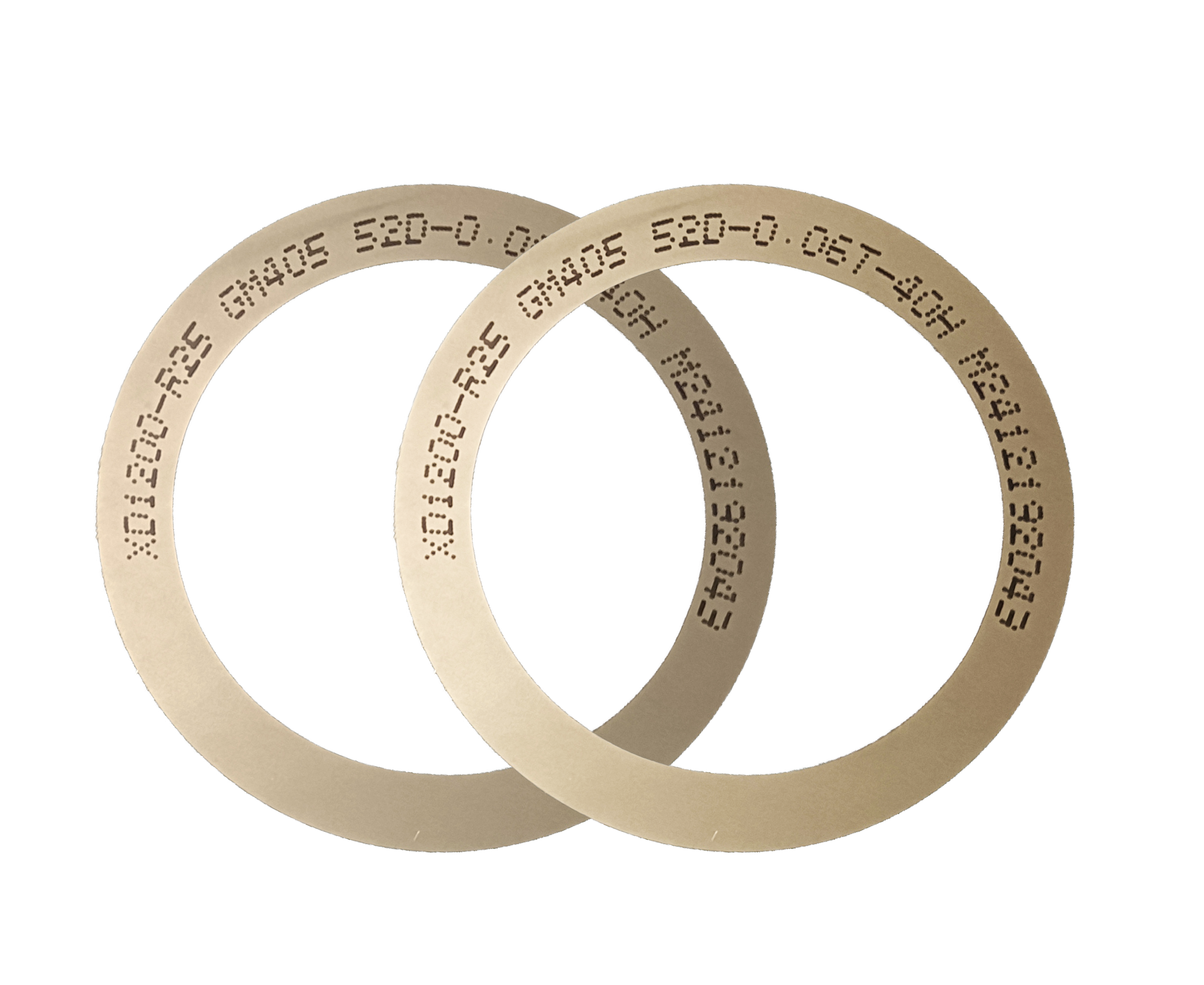
JS Series metal dicing blade — metal bond configurations are used for harder substrates such as SiC.
Conclusion
Sawing blade selection for cleanroom semiconductor dicing is decided by six interlocking parameter clusters: thickness and kerf budget, bond and abrasive construction, cutting accuracy, spindle and feed compatibility, anti-static cleanroom behaviour, and the wear resistance that makes all of it repeatable in mass production. The verified reference points for this platform are an 8 μm–50 μm thickness range with ≤9 μm achieved on ultra-thin programmes, ±0.002 mm cutting accuracy, HRC 65–70 hardness, ≥1.2 mm³/s chip removal rate, and a 30,000–60,000 rpm spindle window operating under Class 100/1000 conditions at 22±2 °C and 45%–55% RH.
Selection works best when it follows one sequence: fix the kerf budget, choose the bond for the substrate, verify accuracy and wear together, confirm the machine and equipment chain, qualify inside the cleanroom environment, and only then scale to volume. Where supply reliability is part of the decision, WINTIME offers a 34,000 ㎡ manufacturing base, a 35-engineer R&D team, annual capacity of 1 million pieces, and mass production of ultra-thin wafer dicing blades as a reference point for how those parameters are held in production.
Next step: request a sawing blade sample or a project quotation with your substrate, kerf budget and target thickness. Email shenxiangfei@ntwintime.com or call +86 13851530812.
Download the full product and capability reference: WINTIME company brochure (PDF). Supplier profile: en.wintime.net.cn. Address: No. 868, Fushou East Road, Rugao City, Jiangsu Province.
Have Questions or Need More Details?
Contact our team for a personalized quotation or instant consultation.
Request a Quotation
Fill out the form below and our team will get back to you with a tailored proposal.
WhatsApp Direct Chat
Prefer to chat in real-time? Message us on WhatsApp for instant assistance & quick answers.
- Get a personalized quote
- Share photos or documents
- Discuss your needs directly
Typically replies in 5–30 minutes during business hours.