
Sawing Blade vs. Laser Cutting for Ultra-Thin Wafers: The Definitive Cost Guide
Ultra-thin wafer dicing rarely fails because a technology cannot cut. It fails because cost per good die stops working at volume. This guide compares the two routes that dominate thin-wafer discussions — mechanical dicing with a diamond sawing blade and laser cutting — and translates kerf loss, knife-edge thickness at or below 9 μm, edge quality and cleanroom conditions into the line items that actually decide a process choice. It also explains why mechanical sawing blades continue to hold the lead in specific dicing applications where die count, dimensional control and stable mass production matter more than the absence of a physical blade.
The comparison is written for process engineers, packaging teams and procurement managers at the awareness and research stage. No single route wins everywhere: the framework matters more than the slogan.
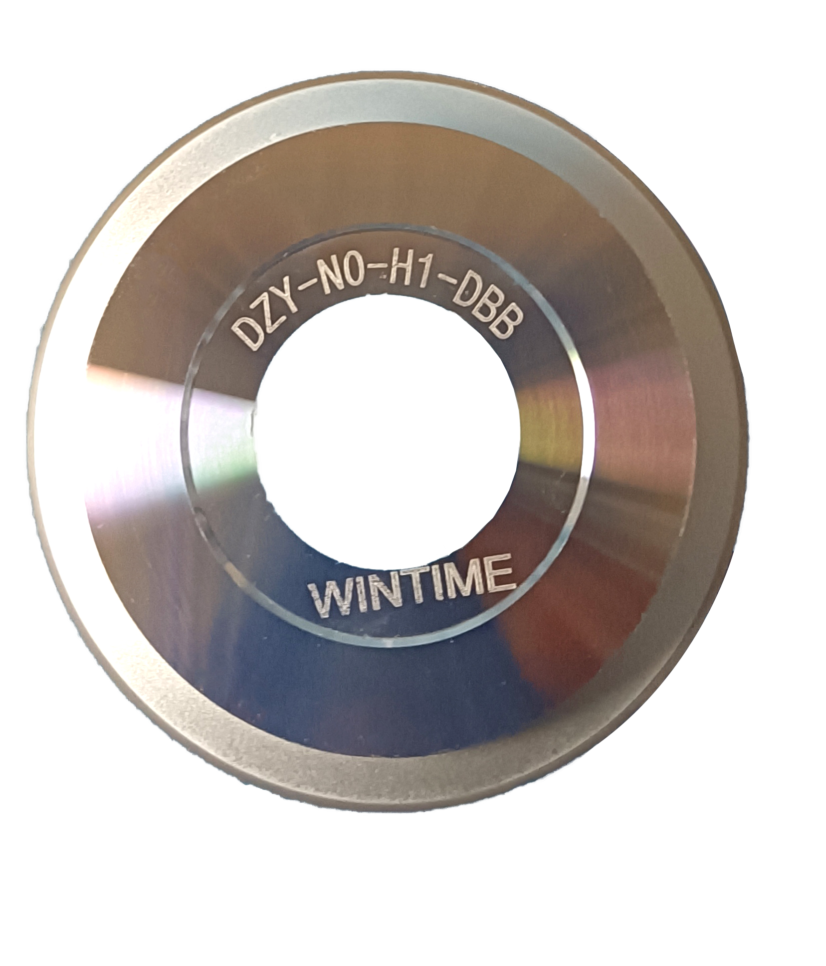
DZY series wafer sawing blade — a blade family used for wafer dicing and scribing on automatic dicing machines.
Problem Definition: Where Ultra-Thin Wafer Economics Break First
At full wafer thickness, dicing cost is mostly a throughput question. Once a wafer is thinned — ultra-thin substrates are commonly referenced at below 50 μm — the economics move to three variables that interact: kerf width, edge quality and handling stability. A wider kerf consumes die area that can never be recovered. A chipped or heat-damaged edge reduces the number of dies that pass test. Unstable handling forces slower feed rates and more operator attention on an expensive tool.
The working metric is cost per good die:
cost per good die = (wafer cost + dicing process cost + consumable cost) ÷ number of dies that pass test
Laser cutting does not change this formula; it changes the values inside it. It removes the physical blade, but it introduces entries of its own — thermal effects at the cut, downstream cleaning, and tool-specific operating requirements. Any comparison built only on blade price versus laser price will misprice both routes.
Industry Background: Scale, Bond Types and the 300 mm Shift
WINTIME Semiconductor Technology Co., Ltd. is a manufacturer established in 2020 that specializes in the research, development, production and sales of high-precision cutting blades, including Sawing Blades and Dicing Blades. The segment it operates in is measurable and large enough to explain why process choice has moved up the procurement agenda:
- The global wafer dicing blade market was valued at USD 1.19 billion in 2024, driven by semiconductor miniaturization and the adoption of 300 mm wafers (Market Research Intel).
- The wider diamond saw blade category, which includes sawing blades for other materials, was valued at approximately USD 8.60 billion in 2025 and is expected to reach USD 10.16 billion by 2032 (Maximize Market Research).
- Resin bond blades held a 42% share of the dicing blade market in 2024, while metal bond blades accounted for 33%, used for harder materials such as SiC (Dicing Blade Market Report 2026, market.us).
- Optical communication and RF/optoelectronics represented 16% of dicing blade market share in 2024, a value of USD 69.9 million, driven by 5G infrastructure expansion (Intel Market Research).
- Hubless dicing blades are increasingly dominant for 300 mm wafer processing because of superior stability and reduced runout on thinner substrates below 50 μm (Semiconductor Equipment Market Data).
- Leading suppliers in the high-precision semiconductor dicing segment include DISCO Corporation, Tokyo Seimitsu (Accretech), Advanced Dicing Technologies (ADT) and Asahi Diamond (Credence Research).
- China's exports of cutting blades grew significantly between 2024 and 2025, with Vietnam increasing by USD 18 million and India by USD 12 million (OEC).
One caution on the numbers: published market-size estimates for dicing blades vary significantly by scope (equipment versus consumables), so they are best read as scale indicators rather than as a forecast for a single product line. What the data does show clearly is that the blade route remains the volume baseline while hubless constructions grow with 300 mm and thin-substrate work.
How Each Process Actually Removes Material
Mechanical dicing with a diamond sawing blade
A sawing blade removes material mechanically. Diamond abrasive is held in a resin or metal bond matrix on a high-strength steel base; the blade rotates on a high-speed spindle and is fed into the workpiece with precision control. The SB-001 sawing blade specification shows the operating envelope: thickness from 8 μm to 50 μm, cutting accuracy of ±0.002 mm, spindle speeds of 30,000 to 60,000 rpm, hardness of HRC 65–70 and a chip removal rate of ≥1.2 mm³/s. Cutting runs dry or wet, and on production lines the blade works on automatic dicing machines in continuous operation with precision feeding.
The cost consequence is predictable and physical: the blade defines the kerf, the blade wears at a knowable rate, and the cut quality depends on bond selection, grit and feed control rather than on material absorption behaviour.
Laser cutting
Laser cutting removes or weakens material with focused energy instead of an abrasive edge. Ablation-type processes vaporize material along the cut; stealth-type processes focus the beam inside the wafer to create a modified layer that is separated afterwards. Both are non-contact, so there is no blade wear and no blade body setting the kerf.
The trade-offs are thermal and material-dependent. Laser processes typically introduce a heat-affected zone and can leave debris or redeposition that requires cleaning, and the achievable result depends strongly on how well the workpiece absorbs the laser wavelength. Whether those effects are acceptable is a per-device question — which is exactly why the decision should be modelled as cost per good die, not as a technology preference.
Step-by-Step: Building a Real Cost-Per-Good-Die Comparison
A credible comparison for ultra-thin wafers follows five steps. Each step produces a number that belongs in the formula above.
Step 1 — Price kerf against die density
Kerf is the material removed by the cut, and die count per wafer scales with it. In mechanical dicing, kerf tracks blade thickness: at the thin end of the documented range a blade can be as thin as 8 μm, and WINTIME's completed Ultra-thin Wafer D Blade project achieved a process thickness of less than 9 microns. Moving from a 30 μm cut to a sub-9 μm cut is a direct change in how many dies a wafer can yield. Laser kerf is set by beam delivery rather than by a physical blade, so it must be taken from vendor process data — never assumed to be identical to a blade's kerf.
Step 2 — Convert consumables into cost per wafer
Blade-based dicing consumes the blade itself, UV tape and mounting film, cleaning chemistry and — in wet cutting — water and filtration. Blade consumption is a function of wear and wafer count, which makes it forecastable. Laser cutting removes blade consumption but not consumable cost: optics, protective films, expansion steps and cleaning remain. Both routes require an automatic wafer dicing machine or laser platform, a semiconductor cutting spindle on the mechanical route, a UV tape mounting machine, wafer cleaning equipment and a wafer testing machine.
Step 3 — Put a number on yield loss
Chipping at the die edge and heat-affected material are both yield losses, but they are detected at different points. Mechanical dicing with a blade held to ±0.002 mm positioning gives a controlled edge geometry that can be inspected immediately after cut. Laser routes may require an additional removal or cleaning step before the same inspection can be trusted. Line up the two inspection sequences and price the extra steps honestly.
Step 4 — Separate shared environment cost from differentiating cost
Both routes typically run in a controlled environment, so cleanroom cost is often shared rather than differentiating. For blade-based dicing the environment window is explicit: a Class 100/1000 clean room, constant temperature of 22±2 °C, constant humidity of 45%–55%, dust-free and anti-static conditions with a high-speed spindle. Treat this as baseline infrastructure, then compare only the costs that genuinely differ between the two routes.
Step 5 — Check throughput and utilization honestly
Throughput interacts with kerf and feed rate, and it also interacts with blade changes and setup time. A tool that is faster but frequently idle during changeover can still lose on cost per good die. Run both routes through the same hourly tool cost and the same utilization assumption before drawing conclusions.
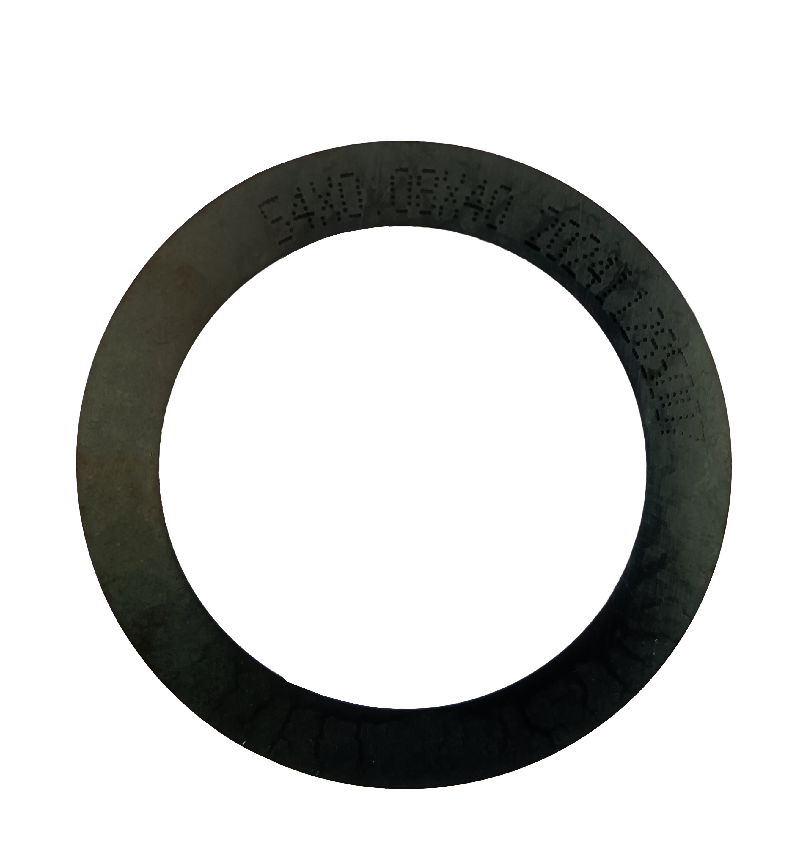
SZ Series resin dicing blade. Resin bond blades held 42% of 2024 dicing blade market share, with metal bond at 33% (market.us).
Knife-Edge Performance: What ≤9 μm Actually Changes
Thin blades are not a catalogue detail; they are the reason several dicing applications still belong to mechanical processing. WINTIME's Ultra-thin Wafer D Blade project reached a process thickness of less than 9 microns, and the company is one of the few domestic companies able to achieve mass production of ultra-thin wafer dicing blades. That distinction matters commercially: a blade that exists in a laboratory and a blade that ships in volume are different procurement items.
- Product thickness range: 8 μm to 50 μm, with a bond matrix of resin or metal, diamond superabrasive and a high-strength steel base.
- Cutting accuracy: ±0.002 mm, with spindle speeds from 30,000 to 60,000 rpm and hardness of HRC 65–70.
- Blade families: Diamond Sawing Blade, Precision Sawing Blade, Semiconductor Sawing Blade, Circular Sawing Blade, Hubbed Sawing Blade, Hubless Sawing Blade, Flanged Sawing Blade, Serrated Sawing Blade, DZY Series Wafer Sawing Blade, DZR Series Sawing Blade and DZR-S Series Slotted Sawing Blade.
- Production base: a 34,000 ㎡ manufacturing facility, approximately 100 staff, 35 engineers in the R&D team, 2 patent technologies, and an annual production capacity of 1 million pieces.
- Background: the 2023 Nantong WINTIME Semiconductor Special Materials Project carried a total investment of nearly tens of millions of yuan, and export business accounts for 30% of total sales across Southeast Asia, East Asia, North America and the European Union.
Buyer reading: a sub-9 μm blade is a kerf-reduction tool. It pays back through extra dies per wafer, not through the blade line item itself.
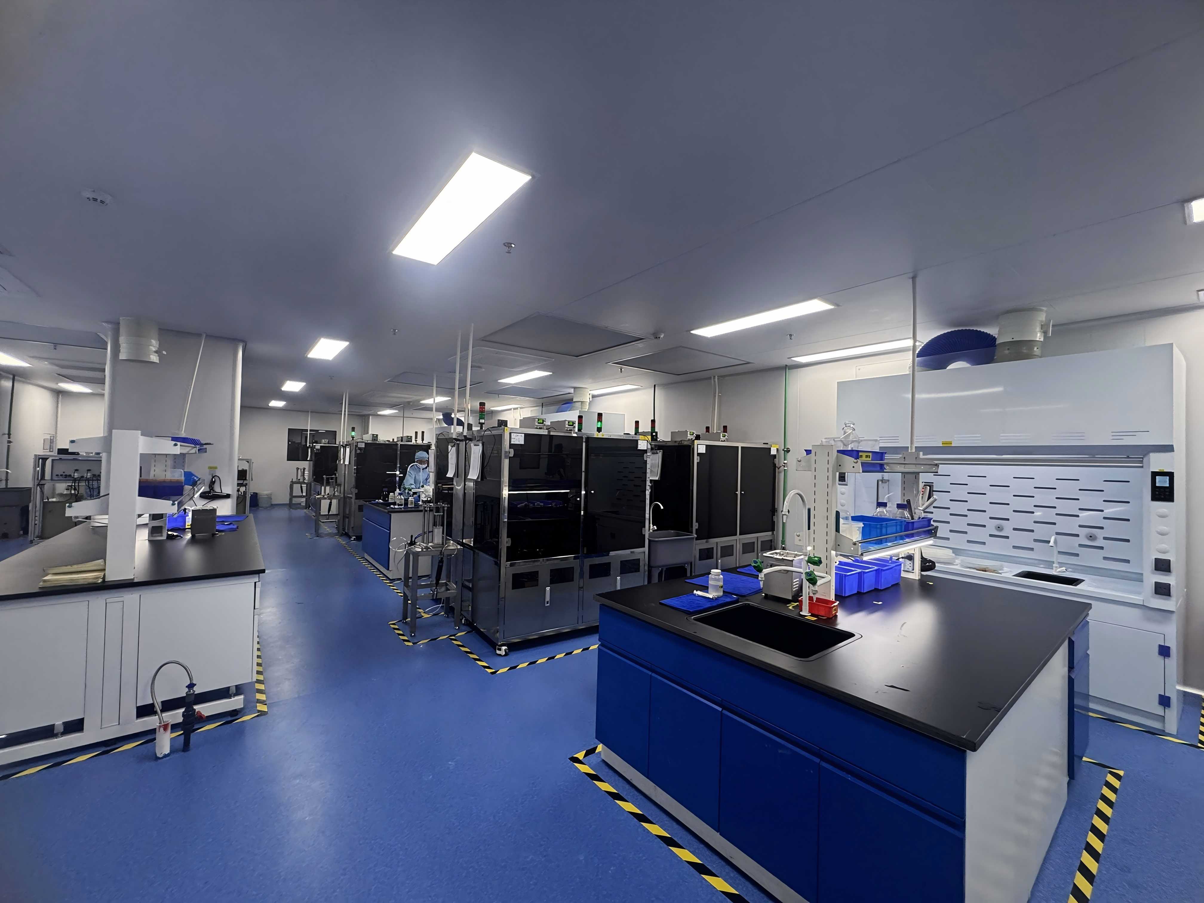
WINTIME production workshop — the company has produced high-precision cutting blades since 2020.
Environment, Compliance and Supporting Equipment
Two compliance layers apply to blade-based ultra-thin wafer dicing, and both affect cost planning.
The first is the product standard: diamond tools, including sawing blades, are categorized under ISO 22180:2019, which distinguishes between CVD diamond-coated types and monocrystalline or polycrystalline types. The second is the operating environment, which is specified separately: a Class 100/1000 clean room at a constant 22±2 °C and 45%–55% relative humidity, in a dust-free, anti-static environment with a high-speed spindle.
Supporting equipment is part of the same cost picture. Blade dicing requires an automatic wafer dicing machine, a semiconductor cutting spindle, a UV tape mounting machine, wafer cleaning equipment and a wafer testing machine. These scenarios are common in China, Japan, Korea, Singapore, Malaysia, the United States and Germany — markets where the installed base of dicing platforms is already in place.
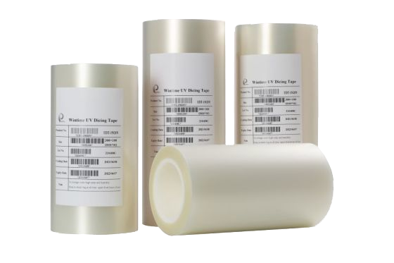
UV film used with UV tape mounting equipment — a consumable line item in both blade-based and laser dicing workflows.
Use Cases: Where the Sawing Blade Keeps Its Lead
Mechanical sawing blades are used in semiconductor manufacturing, semiconductor packaging, precision electronic component processing and optical ceramic cutting, and across optical communication, new functional materials, functional ceramics and alloy materials. The applications where the blade route still leads share a common pattern — established equipment, tight dimensional control, and volume stability:
- Ultra-thin wafer dicing and scribing. Lines already built around automatic dicing machines and high-speed spindles gain die count immediately from a thinner blade, without replacing the platform.
- Semiconductor package cutting. Package singulation rewards repeatable edge geometry and continuous automatic operation more than it rewards non-contact processing.
- Optical device and optical communication cutting. This application group accounted for 16% of dicing blade market share in 2024 (USD 69.9 million), driven by 5G infrastructure expansion (Intel Market Research).
- Functional ceramic substrate cutting. Functional ceramics and new functional materials are established blade applications where bond selection — resin or metal — does the heavy lifting.
- Precision alloy component cutting. Alloy materials and precision electronic components typically favour a defined kerf and a predictable wear curve.
Laser cutting is evaluated in different situations — typically where mechanical contact with a thin or delicate structure is undesirable, or where a material and geometry combination does not suit a rotating blade. That is a project-level decision driven by inspection results, not a universal ranking.
Sawing Blade vs. Laser Cutting: Comparison Table
| Cost / performance dimension | Sawing blade (mechanical dicing) | Laser cutting |
|---|---|---|
| Material removal | Mechanical abrasion by diamond grit held in a resin or metal bond on a rotating blade | Non-contact removal or internal modification by focused energy |
| Tool thickness and kerf | Product thickness range 8 μm–50 μm; process thickness below 9 microns achieved in the Ultra-thin Wafer D Blade project | No physical blade body; effective kerf is set by beam delivery and must be taken from vendor process data |
| Cutting accuracy | ±0.002 mm on the SB-001 sawing blade specification | Platform-dependent; verify positioning specification with the tool vendor |
| Thermal effect at the cut | Dry or wet cutting, with fluid used at the cut in wet mode | Thermal process; heat-affected zone and debris are typical considerations |
| Tool structure and consumables | Diamond superabrasive with resin or metal bond matrix on a high-strength steel base; blade wear is forecastable | No bond matrix; consumables are optics, films and cleaning rather than blades |
| Bond-type market structure (2024) | Resin bond 42%, metal bond 33% of dicing blade market share (market.us) | Not segmented by bond type |
| 300 mm and thin-substrate trend | Hubless dicing blades increasingly dominant for 300 mm processing, with reduced runout on substrates below 50 μm | Not segmented in the published data reviewed |
| Environment | Class 100/1000 clean room, 22±2 °C, 45%–55% RH, dust-free and anti-static with high-speed spindles | Controlled environment generally required as well |
| Supporting equipment | Automatic wafer dicing machine, semiconductor cutting spindle, UV tape mounting machine, wafer cleaning equipment, wafer testing machine | Laser platform plus downstream cleaning and separation steps |
Decision rule: if the platform is already built around a dicing spindle, the wafer is thin, and the material suits diamond abrasion, the blade route usually wins on cost per good die. If contact with the structure is the risk, or the material and geometry do not suit a rotating blade, laser becomes the candidate to qualify. Both routes are governed by ISO 22180:2019 for diamond tools and by the same cleanroom discipline.
FAQ: Sawing Blade vs. Laser Cutting for Ultra-Thin Wafers
Are diamond sawing blades covered by a published standard, and what facility conditions apply?
Yes. Diamond tools, including sawing blades, are categorized under ISO 22180:2019, which distinguishes between CVD diamond-coated types and monocrystalline or polycrystalline types. Facility conditions are specified separately: this sawing blade category operates in a Class 100/1000 clean room at a constant 22±2 °C and 45%–55% relative humidity, in a dust-free, anti-static environment with a high-speed spindle.
Can a sawing blade really process wafers at 9 μm or less?
Yes. WINTIME's completed Ultra-thin Wafer D Blade project achieved a process thickness of less than 9 microns, and the company is one of the few domestic companies able to achieve mass production of ultra-thin wafer dicing blades. The product thickness range runs from 8 μm to 50 μm, with cutting accuracy of ±0.002 mm and spindle speeds of 30,000 to 60,000 rpm, so a sub-9 μm cut sits inside a documented production envelope rather than on a laboratory edge.
Which cost items decide a sawing blade versus laser cutting decision?
Five items decide it: kerf loss (die area consumed by the cut), blade or tool consumption per wafer, yield loss from edge chipping or heat-affected material, facility and consumable cost (cleanroom, UV tape, cleaning, wafer testing), and throughput per hour of tool time. Laser cutting removes blade consumption but keeps cleaning, film and environment cost, so the comparison must be run on cost per good die rather than on tool price.
How can a buyer validate a blade before committing to volume?
Validation starts with the process environment rather than with the blade. The supporting equipment set is an automatic wafer dicing machine, a semiconductor cutting spindle, a UV tape mounting machine, wafer cleaning equipment and a wafer testing machine. With that in place, buyers can request samples and confirm specification fit — blade thickness, bond type, and hubbed versus hubless construction — directly with the manufacturer.
What has to be in place before production timing can be planned?
Production timing depends on the physical chain rather than on the blade alone: the dicing environment (Class 100/1000 clean room, 22±2 °C, 45%–55% RH, anti-static conditions), the supporting equipment set, and consumable readiness such as UV tape and mounting film. Because scheduling and consumable supply vary by project, the practical step is to open that conversation early — WINTIME can be reached by email at shenxiangfei@ntwintime.com, by phone on +86 13851530812, or by WhatsApp on +8618888053207.
Conclusion: Match the Route to the Device, Not to the Trend
For ultra-thin wafers, the honest answer is that both routes can cut — and both carry cost. What separates them is where the cost lands. A diamond sawing blade concentrates cost in kerf, blade wear and yield control, all of which are forecastable, and it delivers documented capability down to a process thickness of less than 9 microns with ±0.002 mm accuracy inside a Class 100/1000 cleanroom environment. Laser cutting removes blade wear but moves cost into thermal management, cleaning and tool-specific process development.
Where the line already runs on dicing spindles, the material suits diamond abrasion, and die count is the dominant economic lever, the sawing blade route continues to lead on cost per good die. Where contact with the structure is the limiting risk, laser deserves a qualification run — but it should be compared on the same five cost line items, not on technology category.
WINTIME Semiconductor Technology Co., Ltd. manufactures Sawing Blades and Dicing Blades for semiconductor manufacturing and packaging, optical communication, functional ceramics and alloy materials, with a 34,000 ㎡ facility and an annual production capacity of 1 million pieces. If you are evaluating a blade route for a thin-wafer project, email shenxiangfei@ntwintime.com or call +86 13851530812 to discuss specification fit, samples and quotations. The full product brochure can be downloaded here: WINTIME Sawing Blade & Dicing Blade Brochure (PDF).

Request a sample, a quotation or the product catalog — WINTIME Semiconductor Technology Co., Ltd., Rugao City, Jiangsu Province.
Have Questions or Need More Details?
Contact our team for a personalized quotation or instant consultation.
Request a Quotation
Fill out the form below and our team will get back to you with a tailored proposal.
WhatsApp Direct Chat
Prefer to chat in real-time? Message us on WhatsApp for instant assistance & quick answers.
- Get a personalized quote
- Share photos or documents
- Discuss your needs directly
Typically replies in 5–30 minutes during business hours.