
Sawing Blades for Semiconductor Manufacturing: An Application Guide to Wafer Dicing
Answer first: a sawing blade used in semiconductor manufacturing is a diamond-abrasive cutting wheel — commonly 8 µm to 50 µm thick — mounted on a high-speed spindle that separates individual dies along the streets of a processed wafer. The blade, not the machine alone, sets kerf width, chipping level, and the mechanical stress each die survives. Choosing one is therefore a constraint exercise: thickness, cutting accuracy, bond type, and hub construction must all match the wafer material, the street layout, and the cleanroom and equipment environment in which dicing takes place.
This guide is written for process engineers, packaging engineers, and sourcing teams who are in the research and evaluation stage of selecting a semiconductor wafer sawing blade. It covers blade construction, the documented specification envelope, the equipment chain surrounding a dicing blade (automatic dicing machines, UV tape mounters, and wafer cleaners), the cleanroom conditions that constrain blade choice, and the commercial variables — minimum order quantity, lead time, and customization scope — that determine whether a specification can actually be supplied at production scale.
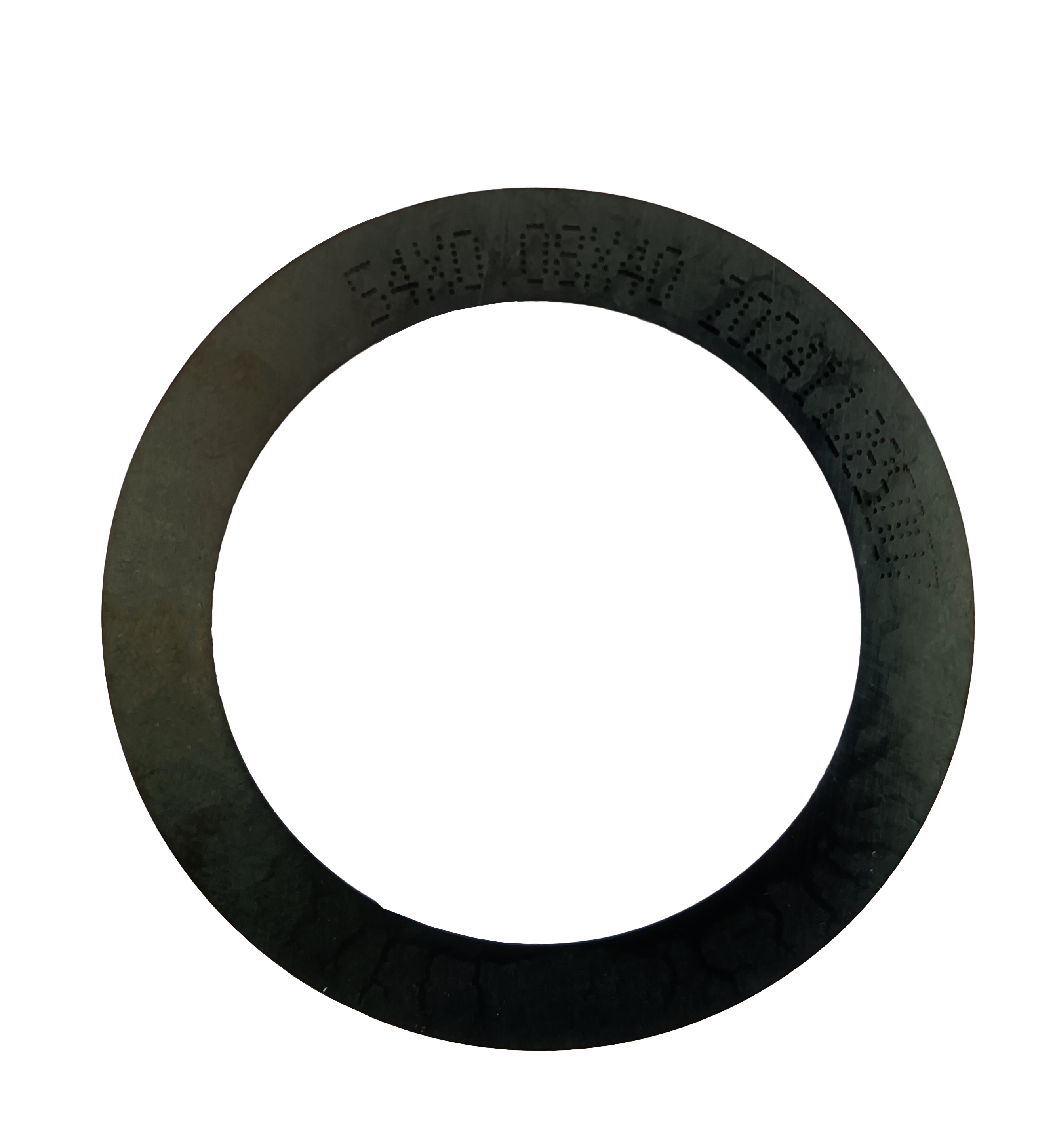
Problem Definition: The Dicing Step Where Yield Is Decided
Wafer dicing is the last mechanical operation performed on a fully processed wafer. Every deposited layer, every device, and every hour of fab time has already been invested. The blade then has to cut through the wafer along streets measured in tens of microns without chipping the device edge, without delaminating sensitive layers, and without leaving particles that survive into packaging. When the blade is mismatched to the application, the failure surfaces as edge chipping, micro-cracks, kerf wander, blade loading, or breakage of ultra-thin wafers — all downstream costs that cannot be recovered.
Four constraints define the search space for a wafer dicing blade:
- Ultra-thin slicing. Thinner wafers and thinner dies demand blades that can be manufactured and used at very low thickness. WINTIME's completed “Ultra-thin Wafer D Blade” project achieved a blade thickness of less than 9 µm in the process, a level the company states only a few domestic manufacturers have reached in mass production.
- Narrow kerf. Kerf is the material removed by the blade. A narrower kerf means more dies per wafer, but it also reduces blade stiffness, so kerf cannot be specified independently of runout and dynamic balance.
- Low chipping and dimensional control. Blade-level cutting accuracy of ±0.002 mm is what keeps street position stable across a full wafer and across a production lot.
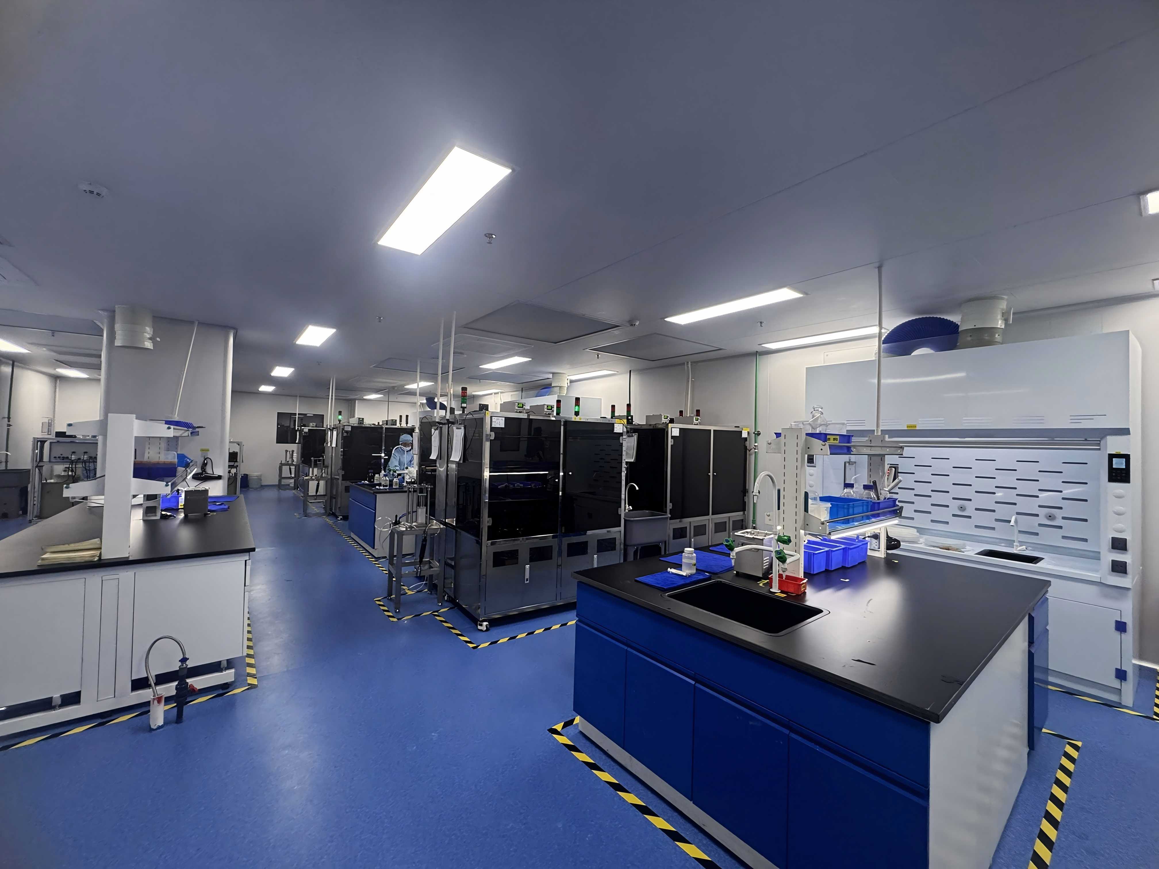
- Cleanroom compatibility. Dicing typically runs in Class 100/1000 cleanrooms at a constant temperature of 22±2 °C and constant humidity of 45%–55%, in a dust-free, anti-static, high-speed spindle environment. Any blade-related contamination, static discharge, or dimensional drift under those conditions becomes a process defect.
The practical problem is rarely the blade in isolation. It is the system: blade plus spindle plus tape plus cleaning plus inspection. A blade that performs well on one tape may load on another; a blade that is dimensionally correct may still produce unacceptable chipping if the feed mode (dry or wet cutting) or the spindle speed is wrong. This is why an application guide, rather than a size chart, is the correct starting document for blade selection.
Industry Background: Where Dicing Blades Sit in the Semiconductor Supply Chain
Dicing blades are a consumable, but they gate a large amount of value. The global wafer dicing blade market was valued at USD 1.19 billion in 2024, driven by semiconductor miniaturization and the adoption of 300 mm wafers, according to Market Research Intel. Published estimates for this market vary by scope — consumables versus equipment — and other sources have placed the figure at USD 1.31 billion and USD 0.437 billion for the same period, so buyers should treat any single number as an order-of-magnitude reference rather than an exact market size.
The broader diamond saw blade category, which includes industrial diamond cutting wheels, was valued at approximately USD 8.60 billion in 2025 and is projected to reach USD 10.16 billion by 2032 (Maximize Market Research). Within the dicing blade segment, construction choice is already polarized: resin bond blades held a 42% share of the market in 2024, while metal bond blades — used for harder materials such as SiC — accounted for 33% (Dicing Blade Market Report 2026).
Two demand patterns matter for application planning. First, optical communication and RF/optoelectronics applications represented 16% of dicing blade market share in 2024, or roughly USD 69.9 million, driven by 5G infrastructure expansion. Second, hubless dicing blades are increasingly dominant for 300 mm wafer processing because of their superior stability and reduced runout on thinner substrates below 50 µm.
On the supply side, the high-precision semiconductor dicing blade market includes established international players such as DISCO Corporation, Tokyo Seimitsu (Accretech), Advanced Dicing Technologies (ADT), and Asahi Diamond, alongside a growing group of manufacturers based in China. Trade data reflects that shift: China's exports of cutting blades to Vietnam, India, and South Korea grew significantly between 2024 and 2025, with Vietnam increasing by USD 18 million and India by USD 12 million (OEC).
WINTIME Semiconductor Technology Co., Ltd. is one of the manufacturers serving this segment from China. Founded in 2020 and based in Rugao City, Jiangsu Province, the company integrates research, development, production, and sales of high-precision wafer-level cutting blades, and also supplies cutting tapes and cutting solutions. Its facility covers 34,000 m², employs approximately 100 people including a 35-engineer R&D team, and has an annual output of more than 1 million dicing blades. Exports account for about 30% of its business, with main markets in Southeast Asia, East Asia, North America, and the European Union.
Detailed Solution: How a Sawing Blade Enables High-Precision Wafer Dicing
Blade architecture: three functional layers
A dicing blade consists of a bond matrix (resin or metal), a diamond superabrasive, and a high-strength steel base. The bond holds the diamond grit in place and wears back at a controlled rate to expose fresh cutting edges; the diamond performs the cutting; the steel core provides the stiffness that keeps the blade running true at high spindle speeds. Bond type is the specification that most changes cutting behaviour, which is why it appears in nearly every blade specification sheet and why resin and metal constructions have developed different market positions.
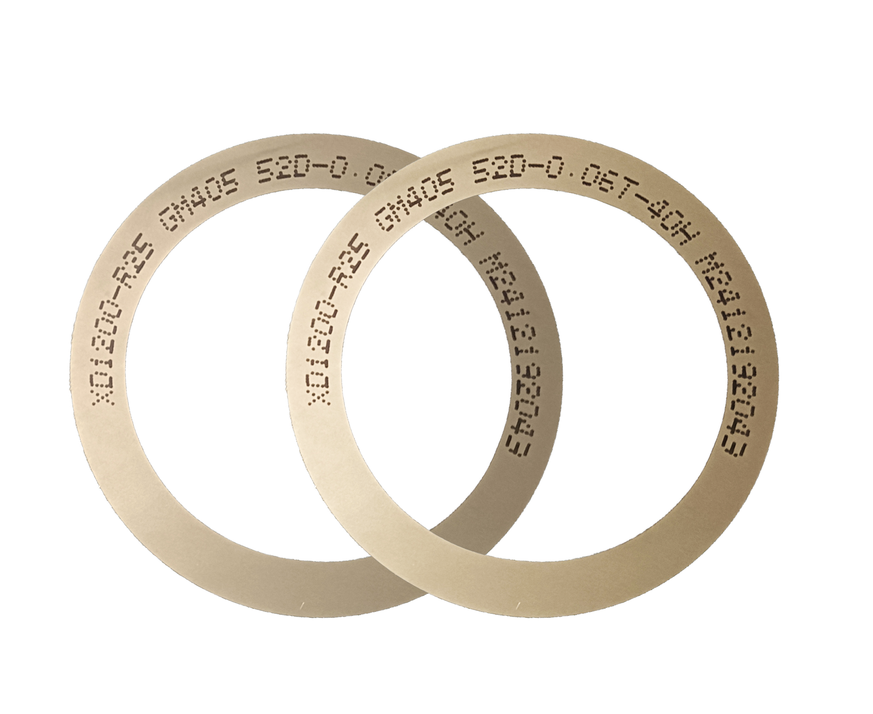
The documented specification envelope
For the WINTIME Sawing Blade range (model SB-001), the published technical parameters define the envelope within which a dicing process can be matched:
| Parameter | Documented value | What it controls in wafer dicing |
|---|---|---|
| Blade thickness | 8 µm – 50 µm | Kerf width and dies per wafer; ultra-thin capability is demonstrated by the completed Ultra-thin Wafer D Blade project at less than 9 µm |
| Cutting accuracy | ±0.002 mm | Street position accuracy and die edge quality across a wafer and a lot |
| Spindle speed | 30,000 – 60,000 rpm | Compatibility with high-speed dicing spindles used in automatic dicing machines |
| Hardness | HRC 65–70 | Wear resistance and blade life across long production runs |
| Bond type | Resin / metal | Cutting behaviour and applicability across different workpiece materials |
| Chip removal rate | ≥1.2 mm³/s | Limits loading, heat build-up, and re-cutting of debris in the kerf |
| Bond matrix | Resin / metal | Grit retention and self-sharpening behaviour |
| Abrasive | Diamond superabrasive | Cutting edge hardness and wear life |
| Base | High-strength steel | Stiffness and runout control at high rotational speed |
Read as a group, these numbers show where the constraints interact. A 50 µm blade is stiff and forgiving but removes more material; an 8 µm blade conserves silicon but leaves very little margin for spindle runout, tape tension, or feed-rate error. The ±0.002 mm cutting accuracy figure is the tolerance that keeps the blade inside the street, and the chip removal rate is the parameter that determines whether debris evacuates or is re-cut into the die edge.
Series and construction coverage
Blade ranges are normally organised by workpiece and cutting problem rather than by dimension alone. The documented range includes the DZY Series Wafer Sawing Blade, the DZR Series Sawing Blade, and the DZR-S Series Slotted Sawing Blade, together with hubbed, hubless, flanged, and serrated constructions and diamond, precision, semiconductor, and circular sawing blade types. Electroforming hard blade construction is used for demanding hard-material work, while application-oriented blades address optical communication components, functional ceramics, and alloy materials — the same three material families that appear alongside semiconductor manufacturing, semiconductor packaging, and precision electronic component processing in the documented applicable-industry list.
For a buyer, the practical meaning is that hub construction, bond type, and thickness should be treated as separate decisions. Hubless sawing blades suit thin substrates and large-diameter wafers where runout matters most; hubbed and flanged constructions provide a different stiffness and mounting profile. Choosing a series first and then forcing the process to fit it is the most common selection error in wafer dicing.
Cleanroom and process compatibility
Cleanroom compatibility is a hard constraint, not a preference. Dicing runs in Class 100/1000 clean rooms at constant temperature (22±2 °C), constant humidity (45%–55%), and in a dust-free, anti-static, high-speed spindle environment. The documented special requirements for this application are an ultra-thin blade thickness of ≤9 µm, high wear resistance, low cutting loss, anti-static behaviour, high dimensional accuracy, long service life, and stable mass production. Operation is by high-speed spindle rotating cutting, in dry or wet mode, with automatic dicing machine continuous operation and precision feeding.
The equipment chain around the blade
A dicing blade is only one element of a matched set. The documented matched equipment for wafer dicing and scribing includes the automatic wafer dicing machine, the semiconductor cutting spindle, the UV tape mounting machine, the wafer cleaning equipment, and the wafer testing machine.
- Automatic wafer dicing machine: indexes the wafer, controls feed rate and cutting mode, and determines whether continuous production can hold the blade within its accuracy window.
- Semiconductor cutting spindle: delivers the 30,000–60,000 rpm rotation range at which blade stiffness, hardness, and dynamic balance are designed to operate.
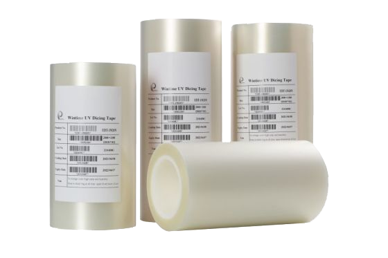
- UV tape mounting machine: fixes the wafer on tape before dicing and releases it afterwards; tape tension and adhesion directly affect chipping and die retention.
- Wafer cleaning equipment: removes debris generated at the kerf, which is the point at which chip-removal behaviour becomes a yield question rather than a blade question.
- Wafer testing machine: confirms that dies remain functional after dicing and cleaning, closing the loop on blade performance.
Step-by-Step Breakdown: Matching a Sawing Blade to a Dicing Process
The sequence below follows the order in which the constraints actually bind. Changing an early step invalidates the later ones, which is why the workpiece is defined first.
- Define the workpiece. Record the wafer material, wafer thickness, die size, street width, and device sensitivity. Bond type, thickness, and feed mode all follow from this. Metal bond blades are the construction associated with harder materials such as SiC, while resin bond constructions represented the larger share of the 2024 dicing blade market at 42%.
- Fix the thickness and kerf target. Choose within the documented 8 µm to 50 µm thickness range. If the wafer or die requires ultra-thin slicing, confirm that the supplier can produce below 9 µm; WINTIME has documented this level through its completed Ultra-thin Wafer D Blade project.
- Select bond type. Resin bond and metal bond behave differently in grit retention, self-sharpening, and wear life. Test on the target material rather than extrapolating from another product family.
- Select hub construction. For 300 mm wafers and substrates below 50 µm, hubless constructions are increasingly dominant because of superior stability and reduced runout. Hubbed and flanged alternatives remain valid where mounting and stiffness requirements differ.
- Verify dynamic balance and runout. Confirm that the supplier performs dynamic balance detection on a high-speed dynamic balance tester, since imbalance is amplified at 30,000–60,000 rpm.
- Confirm dimensional accuracy. Check that geometric dimension inspection uses a vernier caliper and laser diameter gauge, and that the declared cutting accuracy of ±0.002 mm is validated on the delivered batch.
- Match the equipment chain. Validate the blade against the actual automatic dicing machine, spindle, UV tape mounting machine, wafer cleaning equipment, and testing machine — not against a general specification.
- Run a cutting performance simulation. Cutting performance simulation on the actual material, part of the documented quality control process, is the step that converts a catalogue number into a qualified process condition.
- Lock the commercial parameters. Confirm minimum order quantity (50 pieces for standard products, 300 pieces for customized products), lead time (2–5 working days standard, 10–25 working days customized), and packaging before the production schedule is fixed.
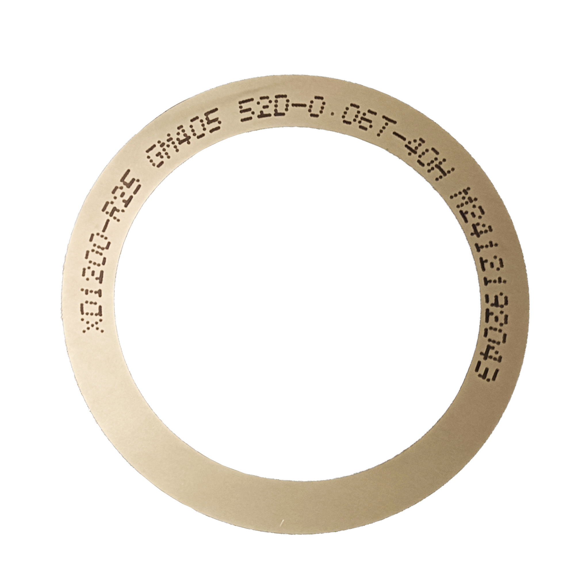
Use Cases: Where These Blade Configurations Are Applied
The documented application scope for this blade family is semiconductor manufacturing, semiconductor packaging, optical communication, new functional materials, functional ceramics, and alloy materials, deployed in China, Japan, Korea, Singapore, Malaysia, the United States, and Germany. The project types that generate demand are consistent across those markets:
- Wafer dicing and scribing in semiconductor manufacturing, where narrow kerf and low chipping dominate blade choice.
- Semiconductor package cutting, where cutting efficiency and dimensional stability across long runs matter as much as edge quality.
- Ultra-thin wafer processing, the case that drives the requirement for blade thickness at or below 9 µm.
- Optical device cutting and optical communication components, a segment that represented 16% of dicing blade market share in 2024, supported by 5G infrastructure expansion.
- Ceramic substrate cutting and functional ceramics, where hardness and brittleness change the bond and grit specification.
- Precision alloy component cutting, where wear resistance and blade life determine the cost per cut.
Across all of these, the documented functional objective is the same: high-precision wafer cutting, ultra-thin slicing, narrow kerf, low chipping, high-efficiency cutting, and stable dimensional control.
Comparison Table: Selection Variables and Documented Evidence
The table below compares the variables a buyer actually chooses between. Only documented figures are used; where a value is not published, the cell states the constraint rather than an estimate.
| Selection variable | Option A | Option B | Documented evidence |
|---|---|---|---|
| Bond type | Resin bond | Metal bond | Resin bond blades held 42% of the 2024 dicing blade market; metal bond blades held 33% and are used for harder materials such as SiC (Dicing Blade Market Report 2026) |
| Hub construction | Hubless | Hubbed / flanged | Hubless dicing blades are increasingly dominant for 300 mm wafer processing, with superior stability and reduced runout on substrates thinner than 50 µm |
| Blade thickness | Ultra-thin, below 9 µm (documented capability) | Standard range, 8 µm – 50 µm | WINTIME completed Ultra-thin Wafer D Blade project; published SB-001 thickness range |
| Cutting accuracy | ±0.002 mm | Not applicable | WINTIME published Sawing Blade parameters |
| Chip evacuation | ≥1.2 mm³/s | Not applicable | WINTIME published Sawing Blade parameters |
| Verification method | Dimensional inspection, hardness/wear test, dynamic balance test, cutting simulation | Supplier declaration only | WINTIME documented quality control process |
Compliance and Commercial Constraints
Classification. Diamond tools, including sawing blades, are categorised under ISO 22180:2019, which distinguishes between CVD diamond-coated types and monocrystalline or polycrystalline types. That standard gives a buyer a common classification language, but it does not cover thickness, accuracy, bond selection, or cleanroom behaviour — the constraints that decide whether a blade works in a specific dicing process. A specification should therefore combine the classification reference with the application parameters.
Facility constraints. For this application the documented operating envelope is a Class 100/1000 clean room at 22±2 °C and 45%–55% relative humidity, with dust-free, anti-static conditions and a high-speed spindle. Blade selection, tape selection, and cleaning procedure all have to be consistent with that envelope.
Commercial variables. There is no single catalogue price band for semiconductor wafer dicing blades, because cost tracks specification and volume. The variables that move cost are bond type, diamond abrasive grain size and concentration, coating selection (anti-rust, heat-dissipation, or wear-resistant), blade geometry including diameter, thickness and spindle hole size, cutting-performance targets such as cutting speed and service life, special-shaped non-standard blade customization, and export packaging. Order quantity changes the commercial structure: the documented minimum order quantity is 50 pieces for standard products and 300 pieces for customized products, with flexibility for long-term cooperative customers.
Supply capability. Documented monthly capacity is more than 800,000 pieces for standard specifications and more than 80,000 pieces for customized and special-shaped products. Documented lead time is 2–5 working days for standard products and 10–25 working days for customized orders, adjustable for large orders. After-sales coverage includes technical support for cutting process matching and equipment adaptation, quality problem investigation and solution within 48 hours, customized after-sales service for bulk procurement customers, long-term supply guarantees and inventory support, product application training for new customers, and replacement and compensation for defective products caused by quality problems.
FAQ: Sawing Blades for Semiconductor Wafer Dicing
1. What standards and classification systems should a sawing blade specification reference?
Diamond tools, including sawing blades, are categorised under ISO 22180:2019, which distinguishes between CVD diamond-coated types and monocrystalline or polycrystalline types. That classification is the starting point for a blade specification, and the application-specific constraints are added on top: blade thickness, cutting accuracy, bond type, hub construction, and cleanroom behaviour. For wafer dicing, those added constraints typically include the Class 100/1000 cleanroom environment, constant temperature of 22±2 °C, constant humidity of 45%–55%, and anti-static operation at high spindle speed. Referencing a standard alone does not qualify a blade for a process; the specification still has to be validated against the actual workpiece and equipment.
2. Can a sawing blade be customized for a specific wafer dicing process?
Yes. WINTIME manufactures on an OEM, ODM, and customized-production basis, and the documented customization scope covers seven variables: blade diameter, thickness and spindle hole size; bond type (metal or resin); diamond abrasive grain size and concentration; coating for anti-rust, heat-dissipation, or wear resistance; cutting performance targets such as cutting speed and service life; packaging including special export packaging; and special-shaped blades in non-standard sizes. The engineering basis is a 35-engineer R&D team, two patent technologies, and a documented capability to reach blade thickness below 9 µm with production cutting accuracy of ±0.002 mm.
3. What determines the cost of a semiconductor wafer dicing blade?
Cost tracks specification and volume rather than a fixed catalogue band. The main drivers are bond type, diamond abrasive grain size and concentration, coating selection, blade geometry (diameter, thickness, spindle hole size), cutting-performance targets, and whether the blade is a standard or special-shaped part. Volume changes the commercial terms as well: the documented minimum order quantity is 50 pieces for standard products and 300 pieces for customized products, with flexibility for long-term cooperative customers. To quote accurately, a supplier needs the workpiece material, target thickness and kerf, spindle speed, and the dicing machine and tape in use.
4. How can a buyer validate a blade before committing to mass production?
Validation starts before the production order. Standard products carry a minimum order quantity of 50 pieces, which allows a pilot lot to run on the actual dicing machine, tape, and cleaning line. WINTIME's documented quality process includes geometric dimension inspection with a vernier caliper and laser diameter gauge, hardness and wear-resistance testing on a material testing machine, dynamic balance detection on a high-speed dynamic balance tester, and cutting performance simulation on the actual material. Technical support for cutting process matching and equipment adaptation, plus product application training for new customers, is provided so that the first run is set up deliberately rather than by trial and error.
5. What lead times and supply capacity should a dicing line plan for?
Standard products ship in 2–5 working days, while customized orders take 10–25 working days, adjustable for large orders. Documented monthly capacity is more than 800,000 pieces for standard specifications and more than 80,000 pieces for customized and special-shaped products, with long-term supply guarantees and inventory support available for bulk procurement customers. Quality problems are investigated and resolved within 48 hours, and defective products caused by quality problems are covered by replacement and compensation. For planning purposes, treat sampling (standard stock, days) and customization (weeks) as two separate timelines, and lock the blade specification before the packaging and assembly schedule is fixed. The full specification set is available in the WINTIME product brochure, and process questions can be sent to shenxiangfei@ntwintime.com.
Conclusion: A Decision Order for Wafer Dicing Blade Selection
The reliable order of decisions is workpiece first, then thickness and kerf, then bond type, then hub construction, then equipment and cleanroom validation — and only then commercial terms. Reversing that order — choosing a series first and adapting the process afterwards — is what produces chipping, kerf wander, and short blade life on ultra-thin wafers. Where the process requires ultra-thin slicing, the supplier must be able to document thickness below 9 µm and accuracy of ±0.002 mm, and to demonstrate dynamic balance and cutting performance testing rather than declare them.
WINTIME Semiconductor Technology Co., Ltd. manufactures high-precision wafer-level cutting blades, cutting tapes, and cutting solutions from Rugao City, Jiangsu Province, with a 34,000 m² facility, annual output of more than 1 million dicing blades, and documented export coverage across Southeast Asia, East Asia, North America, and the European Union. Process engineers and procurement teams evaluating a dicing blade for semiconductor manufacturing can request specification matching through the channels below.
Next Step: Sample, Specification Matching, or Quotation
To evaluate a sawing blade for your dicing process, share the wafer material, target thickness and kerf, spindle speed, dicing machine, and tape in use. Send those details and the team will respond with a matched specification.
Website: en.wintime.net.cn
Email: shenxiangfei@ntwintime.com
Tel: +86 13851530812
WhatsApp: +86 18888053207
Address: No. 868, Fushou East Road, Rugao City, Jiangsu Province, China
Product brochure: Download the WINTIME brochure
Have Questions or Need More Details?
Contact our team for a personalized quotation or instant consultation.
Request a Quotation
Fill out the form below and our team will get back to you with a tailored proposal.
WhatsApp Direct Chat
Prefer to chat in real-time? Message us on WhatsApp for instant assistance & quick answers.
- Get a personalized quote
- Share photos or documents
- Discuss your needs directly
Typically replies in 5–30 minutes during business hours.