
Solving Kerf Drift and Chipping in Ultra-Thin Wafer Dicing: A Sawing Blade Scenario Guide
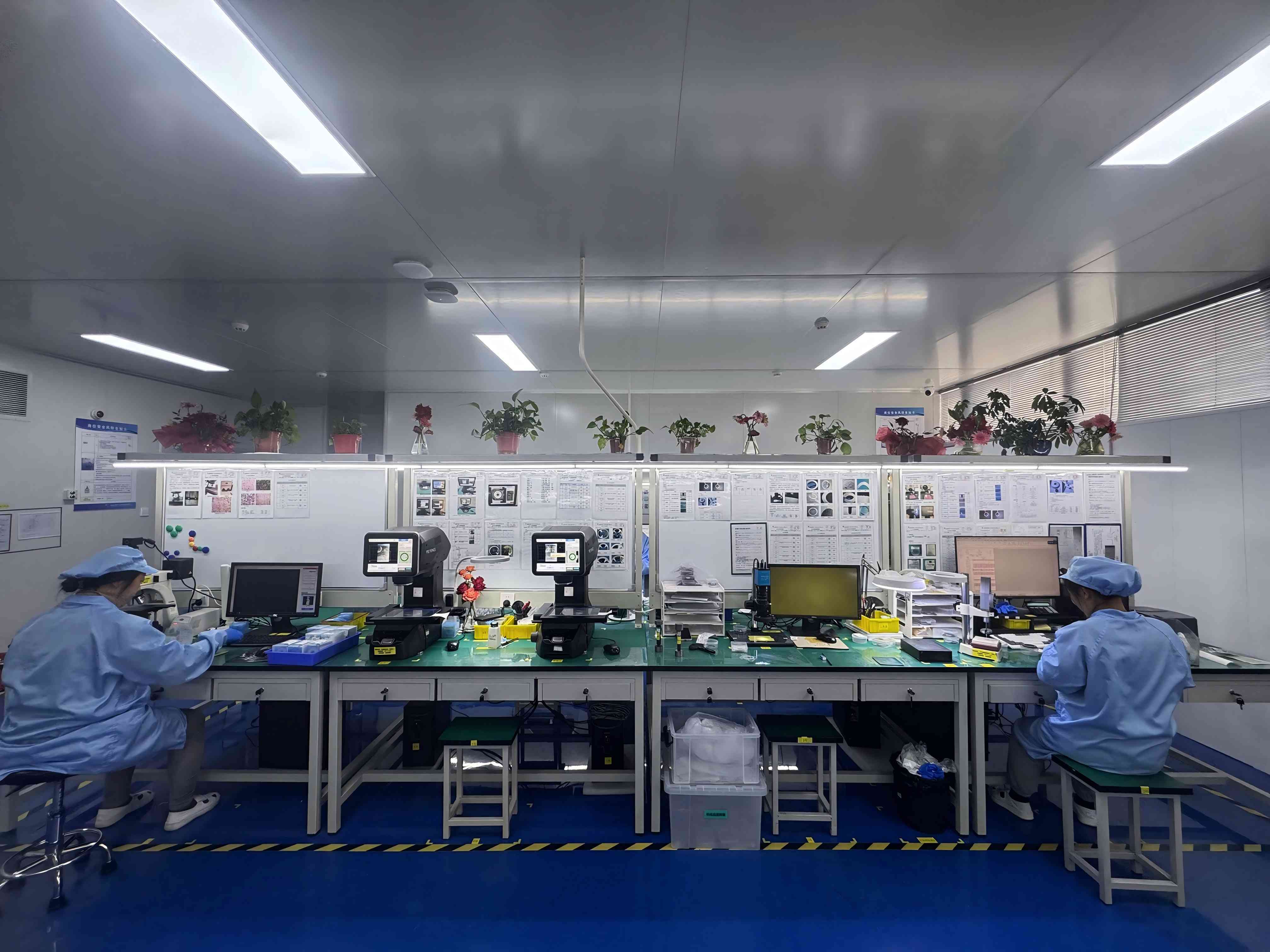
WINTIME's blade production environment, where ultra-thin wafer Sawing Blades are manufactured under standardized process parameters.
Kerf drift and edge chipping are usually treated as two separate yield problems. On ultra-thin wafers they are the same control loop failing at two different scales. The blade decides how much material is removed and how much stress reaches the die edge; the spindle and feed decide how that stress is delivered; the cleanroom decides whether the result repeats from wafer to wafer. This scenario guide explains what causes kerf drift and chipping in ultra-thin wafer dicing, how a Sawing Blade engineered for high-precision wafer cutting holds kerf width and die quality inside spec, and how to lock that performance into a long-term supply agreement.
Problem Definition: Kerf Drift, Chipping, and Unstable Dimensional Control
Kerf drift is the gradual widening or lateral displacement of the cut channel away from its nominal width and position. Chipping is mechanical fracture at the die edge or sidewall. In ultra-thin wafer dicing they rarely appear alone: a blade that has lost dimensional control removes more material than designed, which increases the load on the die edge and produces chipping.
What kerf drift looks like on a production line
- Kerf width creeping outside the nominal window partway through a run rather than at blade break-in.
- Cut lines drifting relative to the street center, so die position tolerance fails before kerf width does.
- Die-to-die dimension variation that passes on the first wafer and fails on the two-hundredth.
- Higher edge-die scrap, because the outermost dies have the least material to absorb drift.
What chipping looks like
- Micro-cracks and spalls concentrated at the blade entry or exit side of the die.
- Chipping that appears after a period of blade wear instead of at the start of blade life.
- Chipping that survives cleaning, which means it is mechanical rather than particle-related.
Why ultra-thin substrates amplify both failure modes
A thinner wafer has less mechanical stiffness, so the same lateral cutting force produces more deflection. There is also less material beneath the street to absorb cutting stress, and the kerf budget is tighter, so a small absolute drift consumes a larger share of the available street width. Static charge becomes a practical concern as well, because thinner dies and tighter spacing leave less margin for electrostatic damage and particle attraction.
The kerf control triangle. Stable kerf width and low chipping are held by three variables at the same time: the blade (thickness, kerf, bond, hub design, wear state), the cut window (spindle speed, feed, dry or wet cutting), and the environment (cleanroom class, temperature, humidity). Changing only one of the three usually moves the defect somewhere else.
Industry Background: Why Dicing Control Is Getting Harder
The demand pressure behind ultra-thin dicing control is measurable. The global diamond saw blade market, the category that includes precision dicing blades, was valued at approximately USD 8.60 billion in 2025 and is expected to reach USD 10.16 billion by 2032 (Maximize Market Research). Within that, the global wafer dicing blade market was valued at USD 1.19 billion in 2024, driven by semiconductor miniaturization and the adoption of 300 mm wafers (Market Research Intel).
Published market sizes for dicing blades diverge, and buyers should read them with the scope in mind: estimates range from roughly USD 0.437 billion to USD 1.31 billion for the same period depending on whether equipment and services are counted alongside the consumable blade. The consumable view is the relevant one for a fab budgeting blade spend.
Two structural trends matter for kerf and chipping control:
- Bond mix. Resin bond blades held a 42% share of the dicing blade market in 2024, while metal bond blades, used for harder materials, accounted for 33%.
- Hubless design. Hubless dicing blades are increasingly dominant for 300 mm wafer processing because of superior stability and reduced runout on substrates thinner than 50 µm.
- Application concentration. Optical communication and RF/optoelectronics applications accounted for 16% of dicing blade market share in 2024, driven by 5G infrastructure expansion.
Sourcing has shifted at the same time. China's exports of cutting blades to Vietnam, India, and South Korea grew significantly between 2024 and 2025, with Vietnam increasing by USD 18 million and India by USD 12 million (OEC). Diamond tools, including sawing blades, are categorized under ISO 22180:2019, which distinguishes CVD diamond-coated from monocrystalline and polycrystalline types.
The Sawing Blade Solution: Five Levers That Hold Kerf and Chipping in Spec
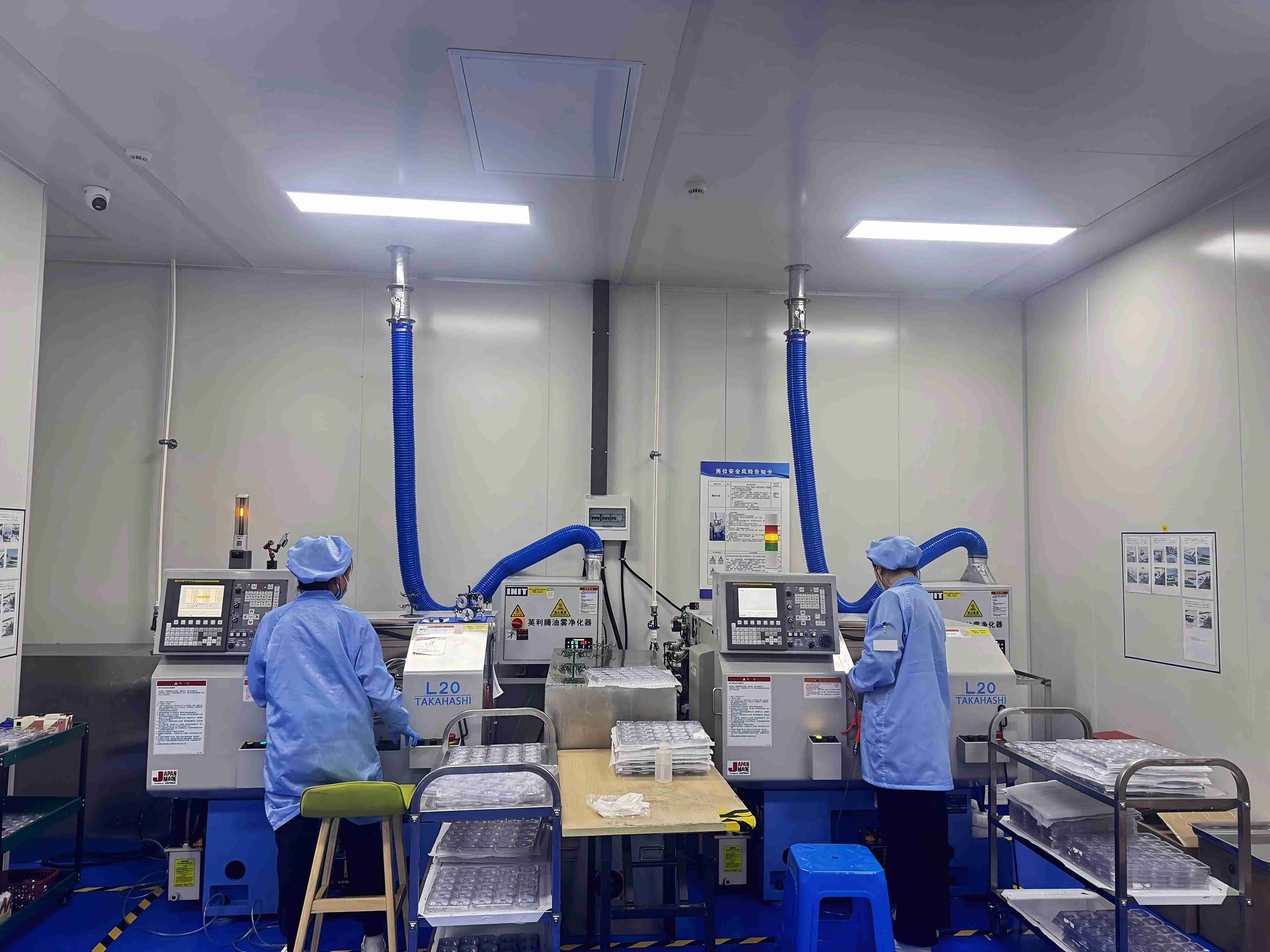
Blade geometry and wear resistance are set during manufacturing, not during cutting: the levers below are decided before the blade reaches the saw.
A Sawing Blade addresses kerf drift and chipping through five design and operation levers. Each one maps to a specific failure mode on the line.
1. Narrow kerf and a thin blade body reduce cutting loss
Narrow kerf means less material removed per street, which reduces the mechanical energy transferred into the die edge and increases the number of dies per wafer. Low cutting loss is therefore not only a cost benefit; it is a chipping-control benefit, because the die edge sees a smaller disturbed zone. Blade families such as the DZY Series Wafer Sawing Blade and DZR Series Sawing Blade are built around this narrow-kerf logic, with the DZR-S Series Slotted Sawing Blade covering profiles that need a slotted geometry rather than a continuous rim.
2. Ultra-thin slicing capability down to a blade thickness of ≤9 μm
Kerf width can never be narrower than the blade body. WINTIME's completed Ultra-thin Wafer Dicing Blade project achieved a blade thickness below 9 μm in process, and the product quality reached the international cutting edge level; WINTIME is one of the few manufacturers in China able to achieve mass production of this class of ultra-thin wafer dicing blade. For a fab chasing kerf drift on a very thin substrate, this defines the floor of what is physically available rather than what is marketed.
3. High wear resistance keeps kerf width stable across blade life
Most kerf drift reports are not blade-defect reports; they are wear reports. High wear resistance keeps diamond exposure and blade diameter stable over a longer cutting distance, so the kerf width measured on wafer one still applies on wafer five hundred. This reduces mid-run parameter chasing and cuts the number of unplanned blade changes, which is where dimensional control is usually lost.
4. Low-chipping geometry and grit control protect the die edge
Chipping is controlled by balancing grit size, diamond exposure, and bond hardness so that material is removed by grinding rather than by fracture. Diamond Sawing Blades and Electroforming Hard Sawing Blades serve different points on this trade-off: electroformed hard blades suit harder substrates where bond retention matters more than free-cutting behaviour. The Semiconductor Wafer Sawing Blade family is the reference point for thin, brittle, high-value devices where chipping has no acceptable level.
5. Anti-static properties reduce an often-ignored defect source
Ultra-thin dies and tight spacing leave little margin for electrostatic discharge. Anti-static blade behaviour reduces charge build-up and particle attraction around the cut, which protects both die quality and the cleanliness of the surrounding area.
Hub choice: hubless Sawing Blades for thin substrates
Hubless Sawing Blades are increasingly dominant for 300 mm processing because they provide superior stability and reduced runout on substrates thinner than 50 µm. On ultra-thin wafers, runout is directly converted into kerf variation, so hub selection belongs in the same decision as blade thickness — not in a separate purchasing step.
Process Window and Cleanroom Conditions: Where Drift Usually Starts

Environmental control is part of the dicing spec, not a facility detail: Class 100/1000 areas held at 22±2 °C and 45%–55% RH give kerf measurements a repeatable baseline.
Blade selection sets the ceiling on kerf control; the process window and the room decide whether that ceiling is reached. Two operating conditions matter most.
- High-speed spindle operation. Higher spindle speeds reduce the load carried by each diamond grit, which lowers edge fracture stress. The blade, spindle, and feed must be matched as one setting rather than optimized separately.
- Dry and wet cutting. Both modes are used in production. Wet cutting manages heat and debris at the cut; dry cutting suits device flows where coolant handling is not acceptable. The choice changes the wear rate, and the wear rate changes when kerf drift appears.
According to the process requirements applied to this blade class, dicing should be performed under cleanroom conditions of Class 100/1000 at 22±2 °C and 45%–55% RH. Temperature and humidity variation changes blade and workpiece dimensions at the micron level, which is exactly the scale at which kerf drift is measured. Particle control protects the die surface; thermal and humidity stability protect the measurement itself.
Step-by-Step Breakdown: A Kerf Drift and Chipping Action Plan
The sequence below follows the order that prevents rework. Each step has one decision and one verification.
- Characterize the failure before changing the blade. Measure kerf width at the start, middle, and end of the cut pattern, and map where chipping occurs. A defect concentrated at entry and exit points is a process-window signal; a defect that grows with blade life is a wear signal.
- Stabilize the environment first. Confirm Class 100/1000 conditions, 22±2 °C, and 45%–55% RH before tuning anything else. If the room is moving, every kerf measurement is a moving target and blade changes will be misdiagnosed.
- Match the blade to the substrate and device. Set blade thickness to the kerf budget, choose hubless geometry for thin substrates and 300 mm wafers, and select resin or metal bond according to material hardness. The DZY Series Wafer Sawing Blade, Hubless Sawing Blade, Electroforming Hard Sawing Blade, Functional Ceramic Sawing Blade, Optical Communication Sawing Blade, and Alloy Material Sawing Blade families exist because one geometry does not cover every substrate.
- Re-tune the cut window. Adjust spindle speed and feed together with the dry or wet cutting mode, then re-measure kerf at the same three points. Change one variable at a time so the result stays attributable.
- Verify across blade life, not on the first wafer. Run kerf width and chipping checks at defined intervals through the blade's working life. The metric that matters is drift rate, not initial kerf width.
- Lock batch consistency into the supply agreement. Standardized process parameters, automatic production equipment, batch production data tracking, and adjacent-batch comparative testing are what keep wafer 10,000 identical to wafer 100. This is also where a long-term partnership replaces a series of one-off purchases.
Long-Term Supply Stability: The Hidden Variable in Kerf Control
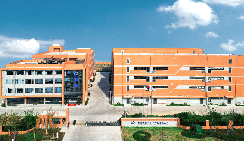
Batch consistency is a manufacturing capability question: WINTIME's Rugao facility covers 34,000 ㎡ with standardized process control and traceable batch records.
A blade that solves kerf drift on a trial wafer only solves the problem if the same blade arrives six months later with the same behaviour. This is why dicing control is partly a supplier-continuity question.
WINTIME Semiconductor Technology Co., Ltd. (brand: WINTIME) is a manufacturer of high-precision wafer-level cutting blades and cutting solutions, founded in 2020 and based in Rugao City, Jiangsu Province, China. The company operates a 34,000 ㎡ facility with 100 employees, including a 35-engineer R&D team, and exports to Southeast Asia, East Asia, North America, and Europe, with exports representing 30% of output. Annual output exceeds 1 million pieces of dicing blades, with a monthly production capacity of over 800,000 pieces for standard specifications and over 80,000 pieces per month for customized and special-shaped products. WINTIME holds 2 patent technologies and applies an ISO 9001 quality management system with standard operating procedures, dedicated quality inspectors, and batch quality files that can be traced and recalled if a batch deviates.
For buyers, three supply-side controls connect directly to kerf performance:
- Batch quality file and traceability. Batch production records allow a drift event to be traced back to process parameters rather than investigated from scratch.
- Adjacent-batch comparative testing. Performance is compared between consecutive batches so that a slow shift in kerf behaviour is detected before it reaches a customer's line.
- Customized capacity. Special-shaped and custom blades run at 80,000+ pieces per month, which supports pilot lines and process-change projects without competing with standard-volume production.
Use Cases: Where These Controls Matter Most
Semiconductor wafer dicing
Thin, high-value wafers are the least tolerant of kerf drift. Narrow-kerf Semiconductor Wafer Sawing Blades combined with hubless geometry for 300 mm processing and Class 100/1000 conditions keep die-edge chipping and dimensional variation inside spec.
Optical communication device dicing
Optical communication and RF/optoelectronics represented 16% of dicing blade market share in 2024, driven by 5G infrastructure expansion. These devices combine brittle materials with tight spacing, so anti-static blade behaviour and low-chipping geometry carry as much weight as kerf width. Optical Communication Sawing Blades are specified for this combination.
Functional ceramic dicing
Ceramic substrates remove material by brittle fracture rather than plastic deformation, so bond selection dominates. Metal bond blades are used for harder materials, and Functional Ceramic Sawing Blades pair that bond logic with narrow kerf to limit edge chipping.
Precision alloy component cutting
Alloy components are cut over longer runs, where wear resistance — not initial kerf width — determines whether dimensions stay stable. Alloy Material Sawing Blades and Electroforming Hard Sawing Blades are used where bond retention and dimensional stability over blade life matter more than free-cutting speed.
Sawing Blade Scenario Comparison Table
| Dicing scenario | Dominant failure mode | Blade-side control | Process / environment control | Documented basis |
|---|---|---|---|---|
| Ultra-thin wafer (under 50 µm) | Edge chipping and kerf drift | Ultra-thin body with blade thickness ≤9 μm, narrow kerf, high wear resistance, anti-static behaviour | Class 100/1000, 22±2 °C, 45%–55% RH; high-speed spindle | WINTIME Ultra-thin Wafer Dicing Blade project achieved blade thickness below 9 μm in process |
| 300 mm wafer processing | Runout and lateral kerf variation | Hubless Sawing Blade for stability and reduced runout | High-speed spindle operation; stable workpiece holding | Hubless dicing blades are increasingly dominant for 300 mm processing on substrates thinner than 50 µm |
| Optical communication devices | Edge cracks and static-related defects | Anti-static, low-chipping Optical Communication Sawing Blade | Dry or wet cutting selection; ESD and particle control | Optical communication and RF/optoelectronics held 16% of dicing blade market share in 2024 |
| Functional ceramic substrates | Brittle chipping and bond wear | Metal bond / Electroforming Hard Sawing Blade for harder materials | Feed and coolant tuning to control fracture | Metal bond blades, used for harder materials, accounted for 33% of the dicing blade market in 2024 |
| Precision alloy components | Kerf drift over long runs | High wear resistance for kerf stability across blade life | Standardized process parameters and batch-level comparison | WINTIME standardized process parameters plus batch production data tracking and adjacent-batch comparative testing |
| Standard vs. customized blade supply | Batch-to-batch performance shift | Consistent geometry and bond from a controlled process | ISO 9001 SOPs, dedicated inspectors, traceable batch quality files | WINTIME monthly capacity: over 800,000 pieces standard, over 80,000 pieces customized and special-shaped |
FAQ: Kerf Drift, Chipping, and Long-Term Sawing Blade Supply
1. What cleanroom conditions and ESD controls should a dicing area hold to keep kerf stable?
Dicing of this blade class should run under Class 100/1000 cleanroom conditions at 22±2 °C and 45%–55% RH. Temperature and humidity stability protect dimensional repeatability at the micron scale where kerf is measured, while particle control protects the die surface. On ultra-thin wafers, anti-static blade behaviour adds a second layer of protection by reducing charge build-up and particle attraction around the cut. If the room drifts, kerf measurements become unreliable and blade changes are made for the wrong reason.
2. Can one supplier deliver both standard and custom ultra-thin Sawing Blades at production scale?
Capacity should be verified in both categories, because standard and customized blades usually run on different lines. WINTIME operates a 34,000 ㎡ facility with a monthly capacity of over 800,000 pieces for standard specifications and over 80,000 pieces per month for customized and special-shaped products, supported by a 35-engineer R&D team and 2 patent technologies. Its completed Ultra-thin Wafer Dicing Blade project achieved blade thickness below 9 μm in process, and the company is one of the few manufacturers in China able to achieve mass production at that level.
3. What are the MOQ, delivery terms, and payment terms for a long-term blade program?
For standard models, the MOQ is 100 pieces per order, and it is negotiable for long-term cooperative customers or bulk purchase plans. For customized models, the MOQ is 500 pieces per order, with flexible MOQ adjustment for small-batch trial orders below 500 pieces at a slight price adjustment based on customization complexity. Delivery terms are FOB or CIF, and payment terms are 30/70. Buyers planning a multi-year program should treat these terms as the commercial frame around the batch-consistency controls described above.
4. How can a line validate performance before committing to a long-term supply agreement?
Validation works best as a staged process. Start with a trial order under the flexible small-batch arrangement, run kerf width and chipping checks at defined intervals through blade life rather than only on the first wafer, and confirm that the drift rate — not just the initial kerf — stays inside your window. Acceptance criteria for this blade class are pre-shipment testing and third-party inspection such as SGS, which gives both sides an agreed reference point before volume commitments are made.
5. What keeps quality consistent across years of supply?
Three controls do the work. Standardized production parameters and automatic production equipment remove manual variability; a batch production data tracking system records all process parameters; and adjacent-batch comparative testing confirms that performance has not shifted. These sit inside an ISO 9001 quality management system with standard operating procedures, dedicated quality inspectors, and batch quality files that can be traced and recalled if a problem occurs. For export buyers in Southeast Asia, East Asia, North America, and Europe — markets WINTIME already serves — that traceability is what makes a long-term blade program auditable. To start a validation run, request a sample or quote directly: email shenxiangfei@ntwintime.com, or reach the team on WhatsApp at +8618888053207.
Conclusion: Fix Kerf and Chipping as One Loop, Then Lock It In
Kerf drift and chipping in ultra-thin wafer dicing are not two problems to be solved separately. They are one control loop: blade thickness and kerf set the physical limit, wear resistance holds that limit across blade life, anti-static behaviour and low-chipping geometry protect the die edge, and the process window plus a Class 100/1000 environment at 22±2 °C and 45%–55% RH make the result repeatable.
WINTIME Semiconductor Technology Co., Ltd. manufactures Sawing Blades and dicing solutions covering Diamond Sawing Blades, Hubless Sawing Blades, DZY Series Wafer Sawing Blades, DZR Series Sawing Blades, DZR-S Series Slotted Sawing Blades, Electroforming Hard Sawing Blades, and application-specific blades for semiconductor wafers, optical communication devices, functional ceramics, and alloy materials. The company was founded in 2020, is based at No. 868, Fushou East Road, Rugao City, Jiangsu Province, China, and exports 30% of its output. Website: https://en.wintime.net.cn.
Next step: send your wafer material, thickness, and target kerf window, and request a Sawing Blade sample or quote for a validation run. Review the full product range and specifications in the WINTIME Sawing Blade brochure (PDF).
Email: shenxiangfei@ntwintime.com · Tel: +86 13851530812 · WhatsApp: +8618888053207 · Address: No. 868, Fushou East Road, Rugao City, Jiangsu Province