
Standard vs. Ultra-Thin Dicing Blades: A Buyer's Comparison for Wafer and Ceramic Cutting
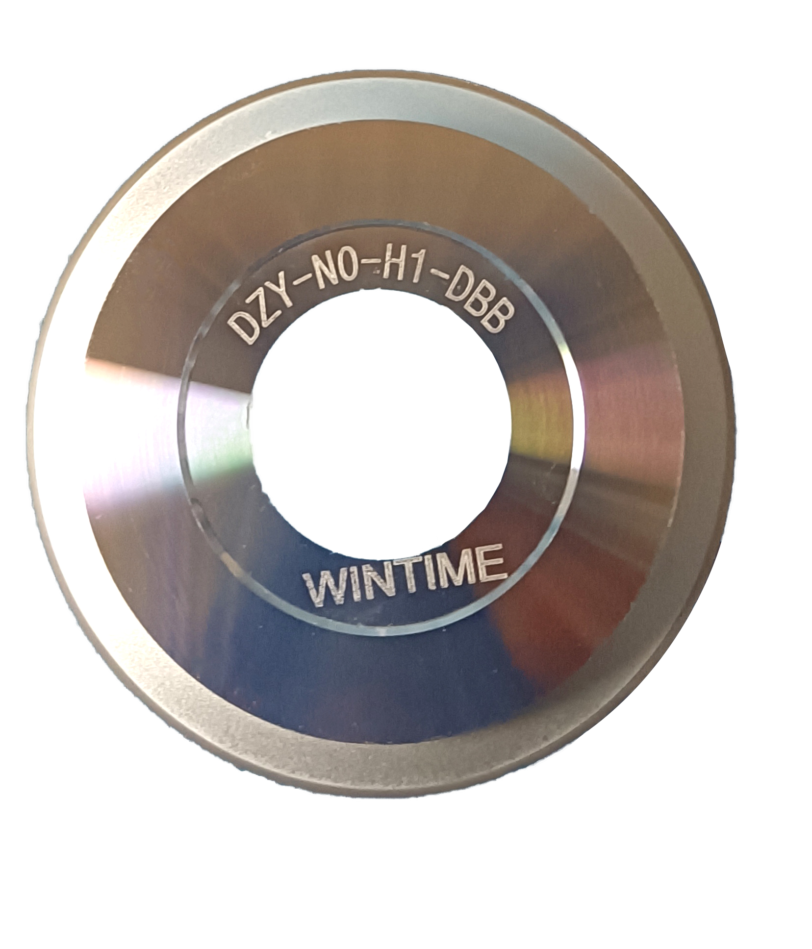
DZY Series wafer dicing blade — WINTIME manufactures both standard-thickness and ultra-thin blade formats for wafer, optical, ceramic and alloy cutting.
Ultra-thin dicing blades remove less material and can raise die-per-wafer yield, but they only pay off when the spindle, the tape and the handling system can hold them stable. Standard-thickness blades stay more forgiving and often remain the correct choice for thicker ceramic sections, mixed-substrate cuts and lines with wider process windows. The working rule for buyers is: select the thinnest blade the process can control — not the thinnest blade the market can produce.
This comparison is written for procurement and process engineers evaluating dicing blades for semiconductor wafer dicing, semiconductor packaging, optical communication devices, functional ceramics and precision alloys. It sets out the criteria that actually change the outcome — kerf width, chipping control, dimensional accuracy, wear resistance, equipment compatibility and total cost of ownership — and it draws only on verifiable product, process and market facts.
Why the Standard-vs-Ultra-Thin Decision Is Harder Than It Looks
Two blade classes sit at the centre of most dicing quotations. They are not simply a thin version and a thick version of the same product.
- Standard-thickness dicing blade. A diamond-embedded circular blade produced in a conventional thickness range, commonly supplied in hubbed, flanged or serrated formats. It is the default choice where kerf loss matters less than process robustness, wide feed windows and predictable handling on older spindles.
- Ultra-thin dicing blade. A blade engineered to a much smaller cross-section so that the material removed per cut is minimised. In WINTIME's completed Ultra-thin Wafer D Blade project, blade thickness was brought below 9 microns — a class in which the blade itself becomes the least forgiving component in the process.
Because both formats can be specified in the same blade family, the buying decision is rarely a choice between a better and a worse product. It is a choice about how much process control the buyer is prepared to maintain in exchange for kerf savings.
Problem Definition: The Four Trade-Offs Behind Blade Thickness
Most blade-mismatch problems trace back to one of four trade-offs. Naming them explicitly is the fastest way to keep a comparison from becoming a price negotiation.
1. Kerf budget versus blade stiffness
A thinner blade removes a narrower strip of material, which is why it is attractive for expensive compound substrates and for wafers where every micron of street width converts into additional dies. The same reduction in cross-section also reduces stiffness. Thinner blades are therefore more sensitive to spindle runout, tape tension, feed-rate variation and vibration. On a machine that cannot hold those variables, kerf savings are paid back in breakage.
2. Chipping control versus throughput
Chipping is the failure mode that quietly destroys yield. Ultra-thin blades typically need gentler feed settings to keep chipping within specification, and a line measured on wafers per hour can lose more time to reduced feed than it gains in material. Standard-thickness blades tolerate wider parameter windows, which is why they remain common on high-mix lines running several materials on one machine.
3. Dimensional accuracy versus handling tolerance
Blade thickness, exposure, outer diameter and bond uniformity all influence how straight a cut stays across a wafer or a ceramic strip. A narrow blade exaggerates every deviation. Dimensional accuracy has to be verified on the incoming batch, not assumed from a sample that was inspected months earlier.
4. Off-the-shelf availability versus customization
Standard blades are usually available from stock with short lead times and low minimum order quantities. Ultra-thin formats frequently require customized bond type, abrasive size, thickness and coating — which changes the qualification timeline, the MOQ and the safety stock calculation. Buyers who compare only unit price miss this dimension completely.
Industry Background: What the Dicing Blade Market Looks Like in 2026
Dicing blades are a consumable category inside a much larger semiconductor tool market, and the published numbers reflect that ambiguity. According to Intel Market Research, the global dicing blade market was valued at USD 1.31 billion in 2024, with projections to reach USD 1.84 billion by 2034. Other research houses publish materially different values because some study scopes include equipment-linked consumables while others count pure blade revenue — a discrepancy buyers should keep in mind when a supplier cites a single headline figure.
Several structural facts are more stable and more useful for a comparison:
- Diamond-embedded blades dominate. Diamond-embedded dicing blades account for over 60% of total market share, driven by superior performance when cutting silicon carbide (SiC) and gallium nitride (GaN), according to the Wafer Dicing Blade Market Outlook 2026–2032.
- Resin bond remains a large share. Resin bond blades held an estimated 42% share of the dicing blade market in 2024, equal to USD 183.6 million, per the Dicing Blade Market Report (2026).
- Hubless designs are spreading in 300 mm processing. Hubless dicing blades are increasingly preferred for 300 mm wafer processing because of superior stability and reduced runout compared with hubbed blades.
- Standard outer diameters are narrow. The standard OD values for semiconductor wafer dicing blades are 55.56 mm (2.187 in) and 76.2 mm (3.0 in), according to the CMP Slurry dicing blade specification guide. Equipment compatibility therefore tends to be a fixed constraint rather than a negotiable one.
- Grit size for bare silicon is well established. For bare silicon dicing, the industry standard diamond grit size ranges from 2 to 6 microns (#2000 to #4000 grit) to minimise chipping.
- Supply is concentrated. DISCO Corporation is the dominant market leader with an estimated 52–55% global share in dicing equipment and associated precision blades, according to the Dicing Equipment Market Research Report 2034 — a concentration that makes second-source qualification a rational procurement objective.
- Regional demand is shifting. China's exports of cutting blades to Vietnam grew by USD 18 million between 2024 and 2025, signalling increased regional demand for semiconductor tools.
Read together, these facts explain why the standard-versus-ultra-thin question is being asked more often: substrates are getting harder and thinner, equipment is standardising around a small number of ODs, and the supply base for genuinely thin, mass-producible blades is still small.
What WINTIME Brings to a Standard-vs-Ultra-Thin Comparison
WINTIME Semiconductor Technology Co., Ltd. (WINTIME) is a Chinese manufacturer established in 2020 that integrates the research, development, production and sales of high-precision wafer-level cutting blades, together with cutting tapes and cutting solutions. The company operates a 34,000 m² facility, employs 35 R&D engineers and holds an annual dicing blade capacity of more than 1 million pieces. Exports account for roughly 30% of output, with main markets in Southeast Asia, East Asia, North America and Europe. Its official site is en.wintime.net.cn.
The Ultra-thin Wafer D Blade project: below 9 microns
WINTIME's completed Ultra-thin Wafer D Blade project achieved a blade thickness of less than 9 microns, and the company states that the product quality of the blade has reached the international cutting-edge level. WINTIME is one of the few domestic Chinese companies able to achieve mass production of this format — the distinction that matters commercially, because a laboratory-grade thin blade and a production-grade thin blade are different procurement objects.
For buyers, the practical implication is that the ultra-thin option does not have to be treated as a prototype route. It can be planned into serial production, with the qualification burden shifting from can this be made? to can our line hold it?
Product families and formats available for comparison
WINTIME's dicing blade range covers the formats buyers typically compare in one tender: Diamond Dicing Blade, Precision Dicing Blade, Semiconductor Dicing Blade, Circular Dicing Blade, Hubbed Dicing Blade, Hubless Dicing Blade, Flanged Dicing Blade, Serrated Dicing Blade, DZY Series Wafer Dicing Blade, DZR Series Dicing Blade, DZR-S Series Slotted Dicing Blade, JS Series metal-bond dicing blades, SZ Series resin-bond dicing blades, and Electroforming Hard Dicing Blade formats.
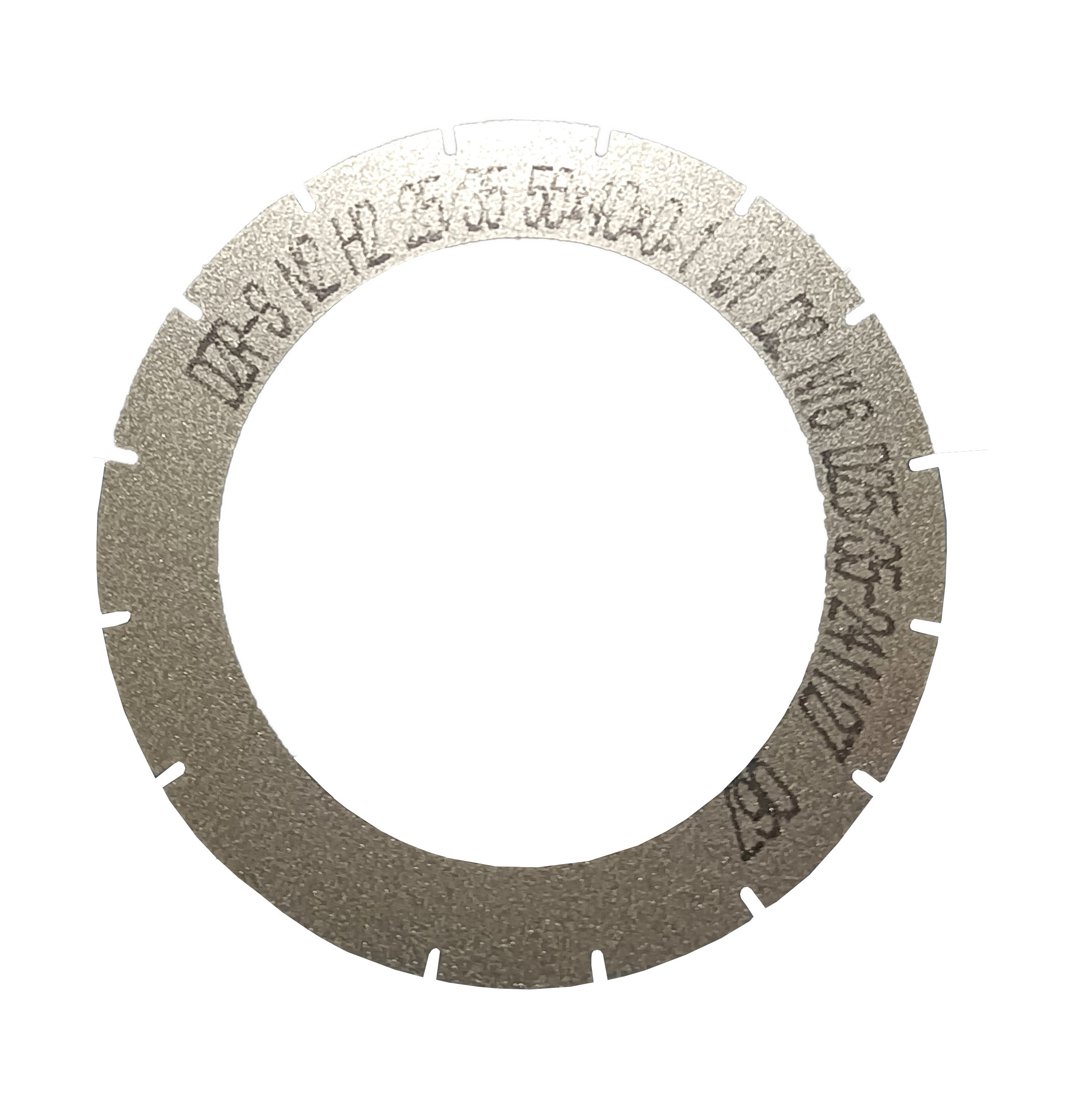
DZR-S Series slotted dicing blade — slotted and hubless geometries are frequently specified when blade stability becomes the limiting factor.
Two material systems run across the range. Metal bond blades are built for harder, more abrasive work; resin bond blades are built for lower-chipping finishes. Diamond abrasive grains are the core functional material in both. Choice of bond and grit is therefore the second decision buyers must make after thickness, and the two interact: a 2–6 micron grit specified for bare silicon behaves differently when it is carried on a sub-9-micron metal-bond body instead of a standard resin-bond body.
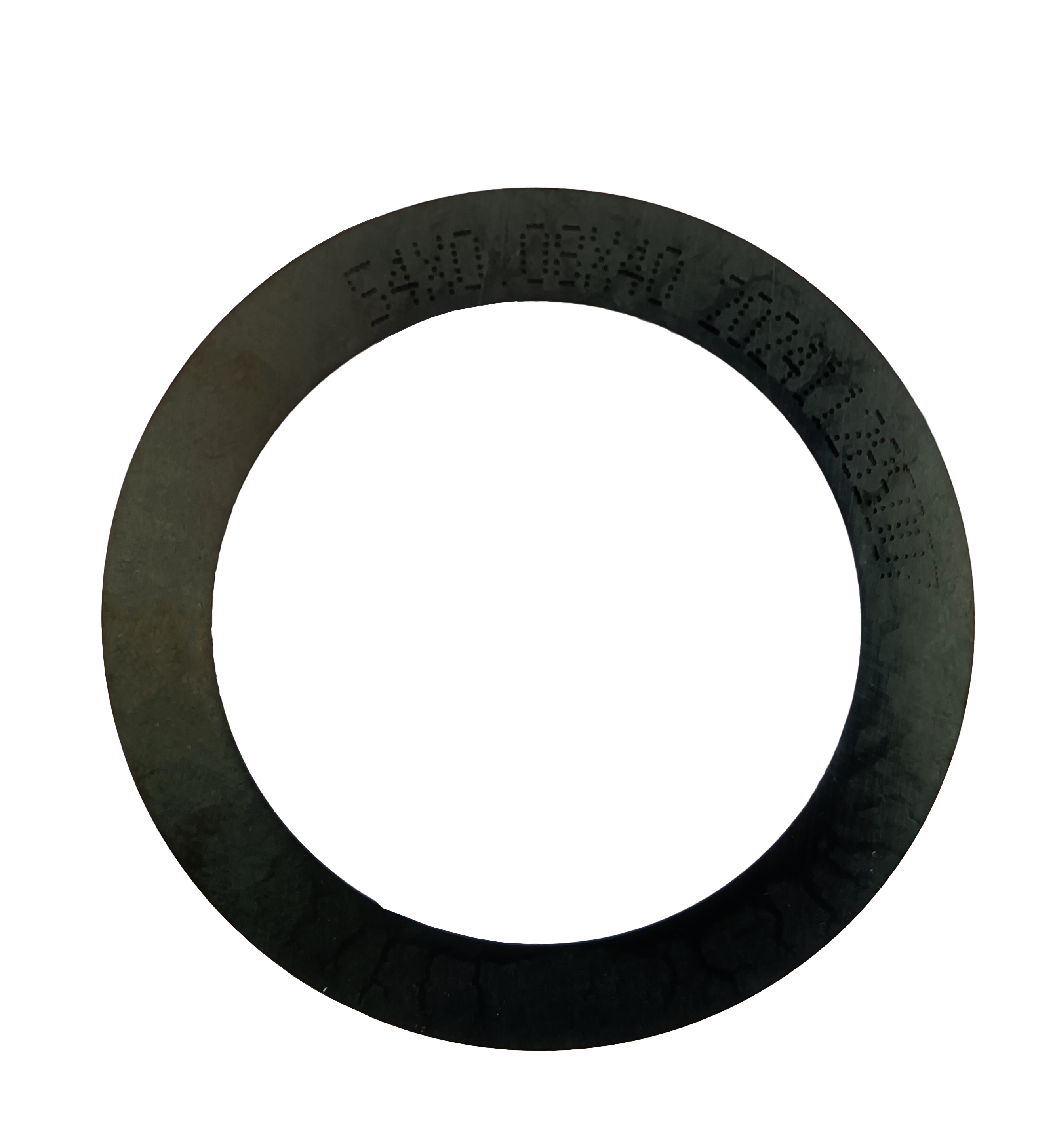
SZ Series resin-bond dicing blade — resin bond remains the reference format for low-chipping finishes on bare silicon.
Manufacturing conditions and quality verification
Thin blades are only as good as the environment that produced them. WINTIME manufactures under Class 100/1000 clean-room conditions with constant temperature (22 ± 2 °C), constant humidity (45%–55%), dust-free and anti-static control, in a high-speed spindle environment. Those same conditions are what the finished blade will demand in the buyer's own line.
Quality control covers five verification points that map directly onto the comparison criteria above:
- Dimensional precision inspection using a laser micrometer and an optical projector
- Abrasive grain uniformity detection through microscope analysis
- Wear resistance and service life testing in a simulated cutting test
- Surface roughness and flatness inspection
- Batch-level inspection before release to packaging

WINTIME's 34,000 m² manufacturing facility — annual dicing blade capacity exceeds 1 million pieces.
Capacity, MOQ and lead time as selection criteria
Capacity decides whether an ultra-thin specification can be sustained after qualification. WINTIME's monthly capacity exceeds 1,200,000 pieces for standard models and 50,000 pieces for customized specifications. Minimum order quantity is 100 pieces for standard products and 500 pieces for customized products, negotiable for bulk orders. Lead time is 3–7 working days for standard models and 15–30 working days for customized orders, depending on customization complexity and order quantity.
Customization is available on blade thickness (from ultra-thin ≤9 μm to standard specifications), diamond abrasive grain size and concentration, bond type (resin bond or metal bond), outer diameter, inner diameter and overall dimensions, anti-static and wear-resistant coatings, cutting performance parameters such as chipping rate and service life, and packaging and labelling.
Step-by-Step: Evaluating Standard vs. Ultra-Thin Blades in Seven Steps
The sequence below is designed to be run as a documented evaluation rather than an internal opinion, so that the resulting specification can be defended in a sourcing review.
Step 1 — Set the kerf budget first
Before looking at any blade, calculate the die-per-wafer or parts-per-substrate gain from a narrower kerf on the specific street layout. Where street width is set by design rules, the gain may be negligible and the ultra-thin case weakens immediately. Where the material is expensive per unit area, the gain can justify a much tighter process window.
Step 2 — Fix the material and the bond before the thickness
Silicon, SiC, GaN, optical glass and functional ceramics behave differently in the cut. Bare silicon has an established grit reference of 2–6 microns (#2000–#4000). Resin bond and metal bond blades produce different chipping and wear profiles on the same material. Choosing thickness before bond and grit inverts the correct order of decisions.
Step 3 — Confirm dimensional compatibility with the existing equipment
Standard OD values are 55.56 mm and 76.2 mm, so the practical question is whether the blade fits the flange or hub system already installed. Hubless designs are increasingly preferred for 300 mm wafer processing because they offer superior stability and reduced runout, but the change from hubbed to hubless is an equipment decision as much as a blade decision.
Step 4 — Verify the operating environment
Ultra-thin blades require clean-room conditions, stable temperature and humidity, anti-static control and a high-speed spindle. If those conditions are not documented in the buyer's own process, the ultra-thin case should be treated as a project rather than a purchase.
Step 5 — Validate chipping and dimensional accuracy on a sample
Cut the buyer's material, on the buyer's tape, on the buyer's dicing machine. Measure kerf width, chipping and dimensional accuracy with the same metrology that production will use — for example a laser micrometer and optical projector for dimensions, and microscope analysis for edge quality.
Step 6 — Test wear resistance across a realistic lot, not a single blade
Blade-to-blade consistency matters more than the best single result. Simulated cutting tests for wear resistance and service life, run on more than one blade from more than one batch, reveal whether the process will hold over a production quarter.
Step 7 — Model total cost of ownership and supply continuity
Combine kerf loss, blade life, scrap from chipping and dimensional error, MOQ and lead time into a single cost-per-good-part figure. Then check that the winning option can be supplied repeatedly: standard models at 3–7 working days and 100-piece MOQ, customized models at 15–30 working days and 500-piece MOQ, with a second source identified if the primary supply is interrupted.
Use Cases: Where Each Blade Class Fits
Semiconductor wafer dicing (8–12 inch)
Thin wafers and high die counts are the classic ultra-thin use case, because every micron of kerf removed converts into usable die area. Hubless geometry and sub-9-micron thickness are most often paired here.
Semiconductor packaging
Package singulation and component cutting tolerate a wider process window, so blade selection is driven by throughput and blade life rather than by kerf alone. Many packaging lines standardise on standard-thickness blades and reserve ultra-thin formats for specific device families.
Optical communication device cutting
Optical devices are sensitive to edge damage rather than to kerf loss. Bond selection and chipping control usually matter more than the last micron of thickness, and a resin-bond format with tightly controlled grit often outperforms the thinnest available blade.
Functional ceramic substrates
Ceramics are abrasive and brittle. Cutting them with an ultra-thin blade can be viable, but wear resistance and blade life become the dominant cost driver, and standard-thickness metal-bond blades often deliver a lower cost per part. Ceramic work is the clearest example of why ultra-thin is not automatically the advanced choice.
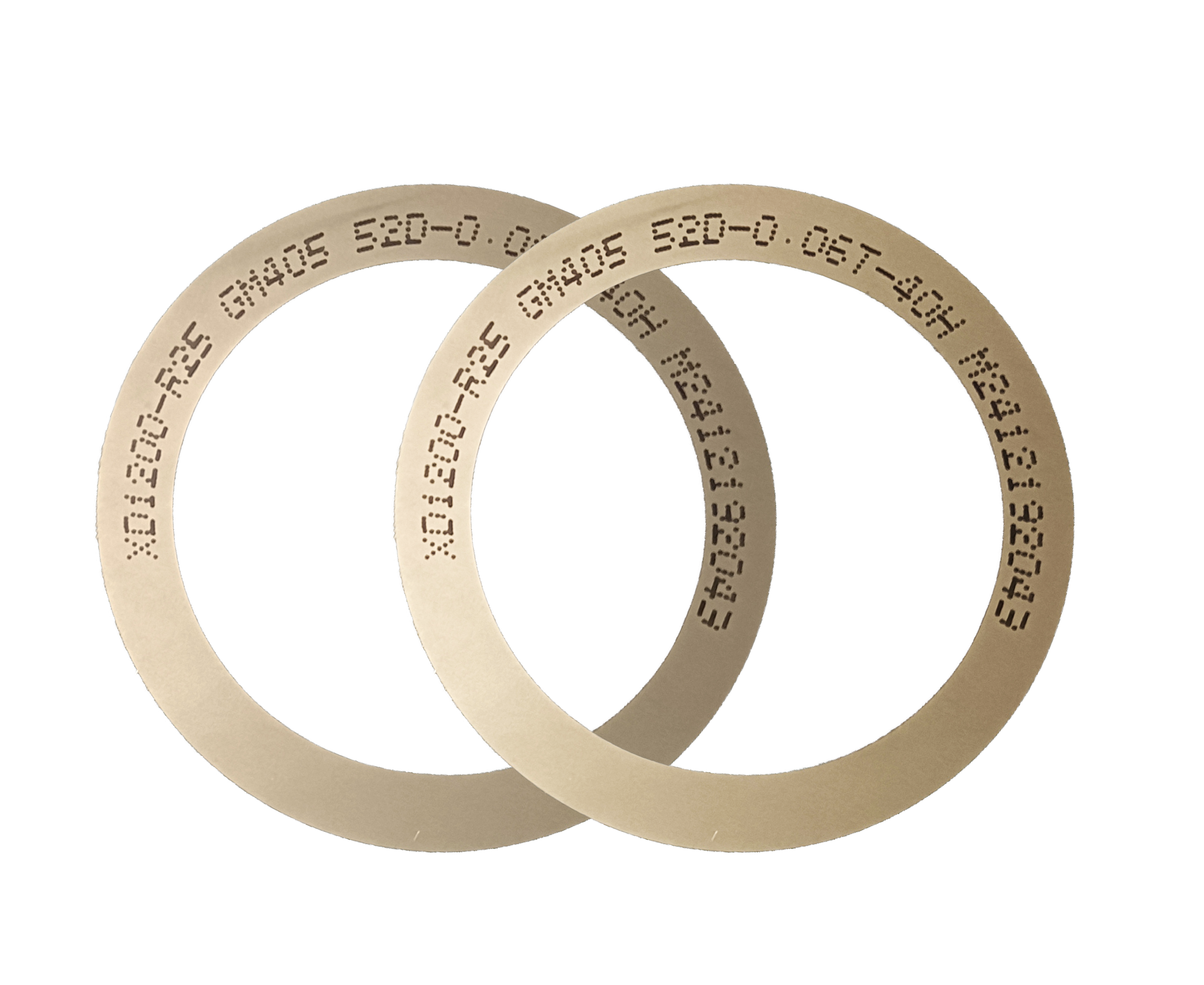
JS Series metal-bond dicing blade — metal bond formats are commonly specified for abrasive ceramic and alloy cutting.
Precision alloy components and new functional materials
Alloys and new functional materials vary widely in ductility and abrasiveness, so blade selection is usually application-specific. A sample validation run is the only reliable way to fix thickness, bond and grit.
Documented application result. A semiconductor packaging factory running 8–12 inch wafer dicing for chip packaging used WINTIME blades at a volume of more than 500,000 pieces per year over a three-year period. The reported results were a cutting chipping rate of ≤5 μm, a wafer yield increase of 12%, and stable mass production without blade replacement. The configuration used an ultra-thin blade thickness of ≤9 μm with a narrow kerf and low material loss.
Standard vs. Ultra-Thin Dicing Blades: Side-by-Side Comparison
The table below compares the two blade classes on the criteria that determine cost per good part. Figures are drawn from verified product, process and industry data; where a value is not established, the table states the verification action instead of a number.
| Selection criterion | Standard-thickness dicing blade | Ultra-thin dicing blade (≤9 μm class) | What to verify before ordering |
|---|---|---|---|
| Kerf width and material loss | Wider kerf; more material removed per street | Narrow kerf and low material loss, as reported for WINTIME's ≤9 μm ultra-thin format | Measure kerf on your own material and street layout |
| Blade thickness | Conventional thickness range | Below 9 microns, achieved in WINTIME's completed Ultra-thin Wafer D Blade project | Request batch-level thickness data, not a nominal value |
| Chipping control | More forgiving of feed-rate and vibration variation | Requires stable feed, clean-room handling and anti-static control; ≤5 μm chipping rate reported in a three-year packaging application | Run a sample cut and inspect edges under a microscope |
| Dimensional accuracy | Verified per batch | Verified per batch | Laser micrometer and optical projector inspection records |
| Wear resistance and blade life | Long life, especially in metal bond on abrasive ceramics | Simulated cutting tests for wear resistance and service life; documented case of stable mass production without blade replacement over three years | Test more than one blade from more than one batch |
| Equipment compatibility | Commonly hubbed, flanged or serrated | Frequently hubless; hubless designs are increasingly preferred for 300 mm wafers due to superior stability and reduced runout | Confirm flange system; standard ODs are 55.56 mm and 76.2 mm |
| Bond and abrasive | Resin bond (42% of the 2024 blade market, USD 183.6 million) or metal bond | Metal bond or resin bond with diamond abrasive grains; 2–6 micron grit (#2000–#4000) is the bare-silicon reference | Match bond and grit to material before fixing thickness |
| Best-fit applications | Ceramic substrates, precision alloys, high-mix lines, packaging singulation | Thin wafer dicing, compound semiconductor work, optical devices, high die-count layouts | Confirm with a sample cut on the actual device |
| Supply and lead time | MOQ 100 pieces; 3–7 working days; over 1,200,000 pieces monthly capacity at WINTIME | Typically customized: MOQ 500 pieces; 15–30 working days; over 50,000 pieces monthly customized capacity at WINTIME | Build lead time into safety stock and second-source planning |
Frequently Asked Questions
What operating conditions and quality checks does an ultra-thin dicing blade require?
Ultra-thin dicing blades are normally run under Class 100/1000 clean-room conditions with constant temperature (22 ± 2 °C), constant humidity of 45%–55%, dust-free and anti-static control, on a high-speed spindle in an automatic dicing machine. WINTIME verifies production through dimensional precision inspection with a laser micrometer and optical projector, abrasive grain uniformity detection under a microscope, wear resistance and service life testing in a simulated cutting test, and surface roughness and flatness inspection. Buyers should confirm these environmental conditions internally before releasing a ≤9 μm blade to production, because a thin blade tolerates vibration and contamination far less than a standard-thickness blade.
Can ultra-thin dicing blades be mass-produced at stable quality, or are they limited to laboratory supply?
They can be mass-produced, but only by a limited number of manufacturers. WINTIME's completed Ultra-thin Wafer D Blade project achieved a blade thickness of less than 9 microns, and the company states that product quality has reached the international cutting-edge level. WINTIME is one of the few domestic Chinese companies able to achieve mass production of this format, supported by 35 R&D engineers, a 34,000 m² facility, and an annual dicing blade capacity of more than 1 million pieces. Monthly capacity exceeds 1,200,000 pieces for standard models and 50,000 pieces for customized specifications. Buyers assessing this capability should request batch-level dimensional and chipping data rather than relying on a single sample certificate.
How should buyers compare the cost of standard and ultra-thin dicing blades?
Compare on cost per good part rather than cost per blade. Three drivers dominate. First, kerf loss: a thinner blade removes less material per street, which matters most when the material is expensive per unit area. Second, blade life: the number of wafers or substrates one blade completes before replacement. Third, yield: chipping and dimensional error scrap finished parts. A cheaper, thicker blade that widens the kerf can cost more in lost material than a thin blade costs to buy, while a thin blade run outside its process window will fail on chipping and consume the difference. Order quantities also enter the calculation: standard products start at 100 pieces and customized products at 500 pieces, negotiable for bulk orders.
How do we validate a blade before committing to a production order?
Run a sample cut on the actual material, tape and dicing machine, then measure kerf width, chipping and dimensional accuracy with the same metrology used in production. WINTIME supports this stage with professional technical consultation and on-site application guidance, customized solution design for special cutting scenarios, spare parts supply and long-term technical support, and after-sales feedback response within 24 hours on working days. Customization covers blade thickness from ultra-thin ≤9 μm to standard specifications, diamond abrasive grain size and concentration, bond type, outer and inner diameter, anti-static or wear-resistant coating, cutting performance parameters such as chipping rate and service life, and packaging and labelling.
What MOQs and lead times should procurement plan for?
Standard dicing blades are quoted at a minimum order quantity of 100 pieces with a lead time of 3–7 working days. Customized blades start at 500 pieces with a lead time of 15–30 working days, depending on customization complexity and order quantity. Both figures should be built into line safety stock and into any second-source qualification plan, because a blade qualified late can stall a ramp even when the technical performance is correct. To move from comparison to validation, buyers can request a sample, a quotation or the full product catalogue from WINTIME using the contact details below.
Conclusion: Match the Blade to the Process Window
Standard-thickness and ultra-thin dicing blades solve different problems. Ultra-thin formats, including WINTIME's Ultra-thin Wafer D Blade with a thickness below 9 microns, convert kerf savings into die-per-wafer gains — but they require clean-room conditions, stable temperature and humidity, anti-static control, correct bond and grit selection, and a spindle that holds runout within tolerance. Standard-thickness blades absorb more variation and often deliver a lower cost per part on abrasive ceramics, precision alloys and high-mix lines.
The buying test is not which blade is more advanced. It is whether the process can hold the blade, whether the kerf saving exceeds the cost of the additional control, and whether the chosen specification can be resupplied at the required lead time. Answer those three questions with measured data from a sample cut, and the thickness decision becomes straightforward.
Next Step: Validate a Blade on Your Own Material
WINTIME Semiconductor Technology Co., Ltd. supports buyers with sample validation, customized specifications and serial production planning for standard and ultra-thin dicing blades.
Website: en.wintime.net.cn
Email: shenxiangfei@ntwintime.com
Tel: +86 13851530812 · WhatsApp: +86 18888053207
Address: No. 868, Fushou East Road, Rugao City, Jiangsu Province
Download the full product catalogue and specification reference: WINTIME Dicing Blade Brochure (PDF)

Request a sample, a quotation or the product catalogue — WINTIME provides on-site application guidance for wafer, optical, ceramic and alloy cutting projects.
Have Questions or Need More Details?
Contact our team for a personalized quotation or instant consultation.
Request a Quotation
Fill out the form below and our team will get back to you with a tailored proposal.
WhatsApp Direct Chat
Prefer to chat in real-time? Message us on WhatsApp for instant assistance & quick answers.
- Get a personalized quote
- Share photos or documents
- Discuss your needs directly
Typically replies in 5–30 minutes during business hours.