
Sub-9µm vs. Standard Dicing Blades: A Head-to-Head Decision for Ultra-Thin Wafers

A dicing blade is usually bought as a consumable. On an ultra-thin wafer it behaves like a process component: its thickness sets how much silicon disappears from every street, and its edge behaviour sets how much of the die edge survives the cut. That is the point at which the comparison between a sub-9µm ultra-thin blade and a standard-thickness blade has to be made on criteria rather than on habit.
This article makes that comparison on the five criteria that actually decide wafer dicing outcomes — narrow kerf, chipping, dimensional control, wear resistance and mass-production stability — and then sets out the conditions under which each class is the defensible choice, a seven-step qualification sequence for a sub-9µm switch, and the questions that separate a real serial supply capability from a demonstration sample.
The short answer
A standard-thickness dicing blade remains the correct default for most wafer dicing work. It is easier to run, easier to source in volume, and its process window is wider. A sub-9µm ultra-thin blade becomes the right choice when two conditions hold at the same time: the kerf of a standard blade consumes street width or die area the product cannot give up, and the wafer stack is thin enough that edge chipping at standard blade thickness becomes a yield risk. When only one condition holds, the decision belongs to process engineering and a cut trial, not to a purchasing switch.
The second half of the decision is supply. A blade that exists as a laboratory sample does not solve a production problem. WINTIME Semiconductor Technology Co., Ltd. is a manufacturer of high-precision wafer-level cutting blades based in Rugao, Jiangsu Province, established in 2020, which reports a completed Ultra-thin Wafer D Blade project that reached a blade thickness of ≤9 µm and states that it is one of the few domestic companies able to mass-produce that class of blade. A documented sub-9µm specification combined with serial production is the benchmark this comparison uses.
Why blade thickness becomes a decision on ultra-thin wafers
Every cut destroys material. Kerf width follows blade thickness, so the material lost per street scales with thickness multiplied by cut length. On a thick wafer the difference between blade classes is a small fraction of the street. On an ultra-thin wafer with narrow streets, the same difference is a larger share of a shrinking budget, and it repeats across every street on the wafer. Geometry alone therefore turns blade thickness into a die-count variable.
The second effect is mechanical rather than economic. Ultra-thin wafers carry less bulk to resist the cutting force, and edge chipping is not a cosmetic defect: a chip at the die edge becomes a stress concentrator in the finished device. Buyers of thin-wafer products therefore judge a blade by the chip distribution it produces, not only by the kerf it leaves.
One boundary matters before any comparison is drawn. Thickness is one lever among several. Bond system, diamond grain size and concentration, exposure, spindle parameters, tape and coolant all move the same outcomes. A head-to-head on thickness alone can produce a misleading result if the other variables are not held constant — which is why the qualification sequence later in this article fixes the wafer stack first and changes the blade second.
Industry background: why this comparison is requested more often
Published market sizing for dicing blades is modest but not static. Business Research Insights estimated the global dicing blade market at USD 0.39 billion in 2026, with a compound annual growth rate of 2.9% through 2035 (report dated August 2026). That figure should be read as a sizing convention rather than a precise consumption measure: published estimates for this category differ partly because some count semiconductor wafer blades only, while others include broader consumable cutting categories.
Behind the slow headline number sits a faster change in requirements. As device designs move toward thinner wafers and tighter streets, more procurement teams ask suppliers for sub-9µm capability than did a few years ago. Supply has responded unevenly. Presenting a thin blade sample is a different capability from producing that thickness repeatably across batches, holding flatness and thickness tolerance, and shipping in the quantities a packaging line consumes. The gap between those two capabilities is where most disappointing ultra-thin blade projects originate.
The five criteria that decide the comparison
1. Narrow kerf and material loss
Kerf is the material the blade removes permanently. A sub-9µm blade is specified at or below 9 µm in thickness, so the kerf it can produce is correspondingly narrow; a standard-thickness blade removes a wider strip from every street. For a given die size and wafer diameter, a narrower kerf leaves more silicon available for die, which is the economic argument for the ultra-thin class.
Kerf is nevertheless not identical to blade thickness. Run-out, vibration and dressing condition widen the cut, so a thickness specification is an input, not a guarantee. The verification step is a kerf measurement on the buyer's own wafer, compared against the street width minus the die-edge margin the design allows.
2. Chipping at the die edge
Chipping is where the two classes separate most sharply in practice. The sub-9µm class exists largely because thinner sections produce lower cutting resistance and a cleaner edge on thin wafers. WINTIME reports that in a three-year project with a semiconductor packaging factory in China, the cutting chipping rate was ≤5 µm while dicing 8–12 inch wafers for chip packaging.
Standard-thickness blades deliver acceptable edges across many thicker-wafer and wider-street applications, and their greater section is easier to control inside a looser process window. The honest comparison is therefore a chip-size distribution measured on the actual stack — wafer thickness, metallization, dielectric layers and tape — not a catalogue figure.
3. Dimensional control
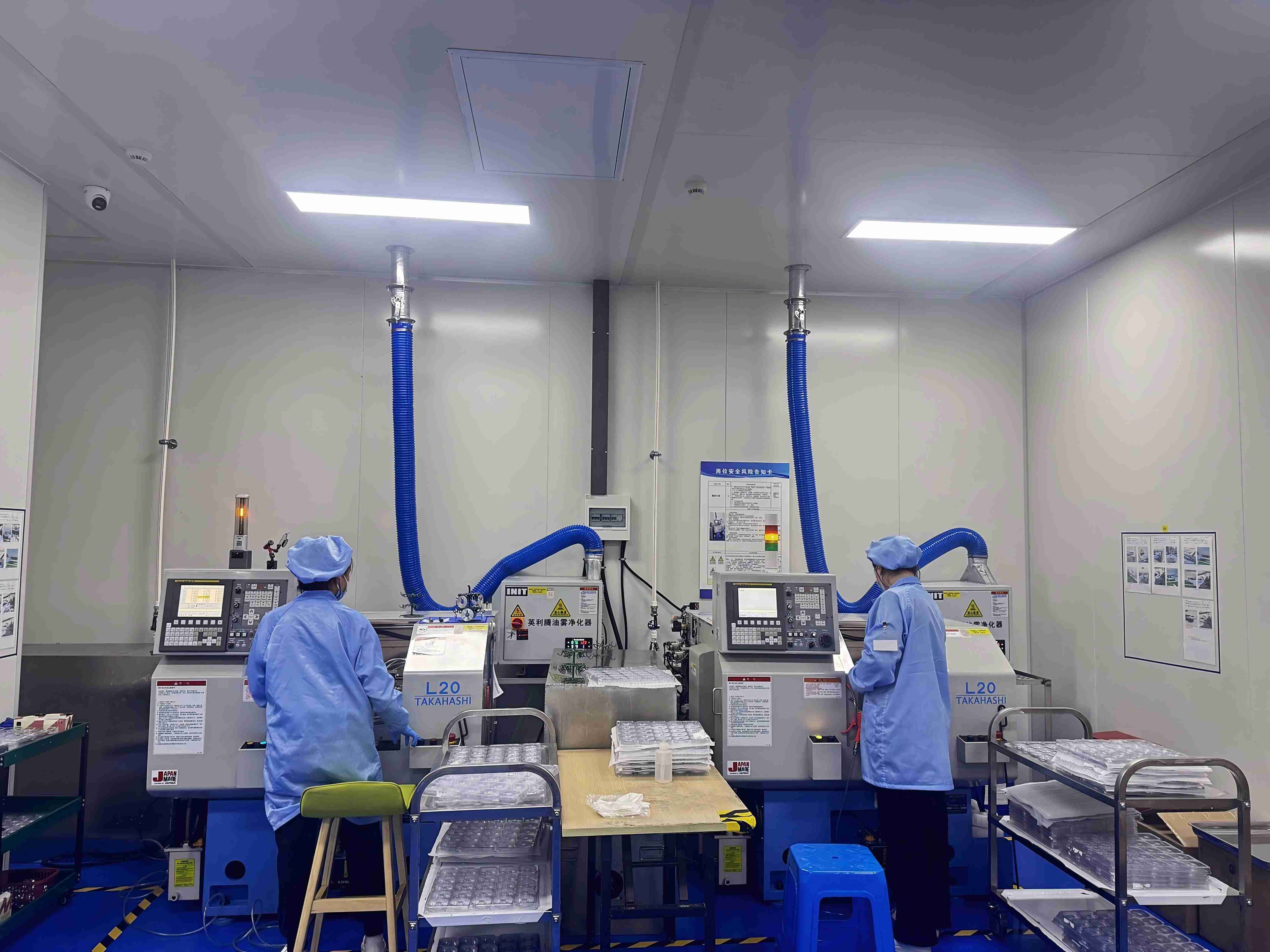
Thin sections are less forgiving. A thickness variation that is a small percentage of a standard blade is a larger percentage of a sub-9µm blade, and flatness and edge geometry have less material to work with when the section shrinks. Buyers should ask which instruments the supplier uses and what the batch records actually show. WINTIME's stated quality control covers dimensional precision by laser micrometer and optical projector, abrasive grain uniformity by microscope analysis, surface roughness and flatness inspection, wear resistance and service life by simulated cutting test, and batch-level quality checks.
4. Wear resistance and blade life
A thinner blade carries less abrasive material, so life depends more heavily on bond type, grain size and concentration, and on how the blade is dressed and loaded. The practical measure is not a vendor life figure but stability across a production run: kerf drift, spindle load trend and edge-quality trend. In the same three-year packaging project, WINTIME reports stable mass production without blade replacement at more than 500,000 pieces of annual blade usage. That is a project result rather than a general guarantee, and it should be reproduced on the buyer's own line before it is treated as a planning assumption.
5. Mass-production stability
This criterion is about the supplier rather than the blade. Batch-to-batch consistency, capacity, lead time and change control determine whether a sub-9µm specification survives contact with a production schedule. WINTIME reports a 34,000 m² facility, annual capacity above 1,000,000 pieces, and monthly output of more than 1,200,000 standard pieces and 50,000+ customized pieces. Whether those figures matter to a specific buyer depends on order size, but the question to ask is always the same: what happens at batch five hundred, not at batch one?
Head-to-head comparison
The table compares the two classes on the criteria above. It sets out documented characteristics and the checks that convert them into evidence; it does not assert that one class outperforms the other on a given wafer without a cut trial.
| Criterion | Sub-9µm ultra-thin blade | Standard-thickness blade | What to verify on your line |
|---|---|---|---|
| Kerf and material loss | Narrower kerf by construction; blade thickness specified at ≤9 µm | Wider kerf for the same cut length | Measured kerf against street width minus die-edge margin |
| Chipping | Designed for low chipping on thin wafers; project-reported chipping ≤5 µm on 8–12 inch packaging wafers | Acceptable on many thicker-wafer, wider-street applications; risk rises as streets narrow | Chip-size distribution measured on your wafer stack and tape |
| Dimensional control | Less section margin; thickness tolerance and flatness harder to hold | More section margin; wider tolerance headroom in the cut | Metrology method used and batch records provided |
| Wear resistance and life | Life sensitive to bond, grain and load; project reported no blade replacement across a three-year run | Greater section margin generally easier to sustain over long runs | Tool-wear log: kerf drift, spindle load and edge trend |
| Process window | Narrower; parameters must be fixed and monitored | Wider; more forgiving during ramp and product-mix changes | Design-of-experiment before production ramp |
| Volume availability | Fewer suppliers can produce it in serial volume; WINTIME reports mass production of the ≤9 µm class and 50,000+ customized pieces per month | Widely available; WINTIME reports more than 1,200,000 standard pieces per month | Batch records, capacity statement and committed lead time |
| Customization room | Thickness, diamond grain size and concentration, bond type, dimensions, coating, cutting parameters and packaging | Same customization categories; generally faster to iterate | Written specification plus first-article approval |
| Typical fit | Narrow streets, thin wafers, high-value die, kerf-sensitive layouts | Thicker wafers, wider streets, mixed-product lines, processes still ramping | Cut trial plus cost-per-die calculation |
Where a standard-thickness blade is still the right call
Choosing a standard blade is not settling for less. It is declining to pay for process discipline the product does not need. Four situations normally point that way:
- Streets wide enough to absorb the kerf. When the layout already allows a wider cut without losing die, kerf economy delivers little and the thinner blade adds cost and complexity for no return.
- Wafer stacks that tolerate standard-section chipping. If measured chip depth at standard thickness stays inside the die-strength requirement, the thinner class has nothing to improve.
- Mixed-product lines. One forgiving parameter set across several products reduces changeover risk and operator error, which often outweighs a marginal kerf gain on one product.
- Processes still ramping. While parameters are still moving, a wider process window is an asset; lock the process first, then consider the thinner class.
The reverse is equally true: a standard blade should not be retained on a narrow-street, thin-wafer product simply because it is familiar. Familiarity is not a process capability.
Where a sub-9µm blade becomes the requirement
Four conditions justify the move. Each must be confirmed on the buyer's own wafer rather than inferred from a specification sheet:
- The street budget fails. Street width minus die-edge margin leaves no room for a standard kerf without sacrificing die.
- Edge quality fails. Chip depth measured on the finished device structure approaches the limit set by die strength or downstream assembly.
- Die value justifies the discipline. On high-value die, a recovered fraction of a street across the wafer changes die per wafer in a way that pays for tighter parameter control.
- The process is mature enough to run narrow. Parameters are locked, monitoring is in place, and the line can hold a narrower window without constant intervention.
The same logic explains why the two classes often coexist inside one factory: the thin-wafer product runs sub-9µm, the rest of the portfolio runs standard, and neither line inherits the other's constraints.
Use cases: matching the blade class to the project
8–12 inch wafer packaging dicing
This is the application with the clearest documented record in this comparison. In a three-year project with a semiconductor packaging factory in China, an ultra-thin blade at ≤9 µm thickness was used for high-precision dicing of 8–12 inch wafers. The reported project results were a cutting chipping rate of ≤5 µm, a wafer yield increase of 12%, annual blade usage above 500,000 pieces, and stable mass production without blade replacement. These are the outcomes of one customer project, not a promise of identical results elsewhere; they show what the class made possible under documented conditions.
Optical communication components
Optical communication dicing puts the emphasis on edge quality and dimensional repeatability, because the cut face and the die edge both carry optical function. The five criteria still apply, but their weighting changes: chipping and dimensional control usually outrank kerf economy. Whether a sub-9µm blade suits a specific component depends on its geometry and on the supplier's demonstrated capability in that application, which has to be verified through a trial rather than assumed from the wafer-dicing record.
Functional ceramics
Functional ceramic dicing does not follow the thin-silicon logic. The workpiece is hard and brittle, the chipping mechanism differs, and bond and abrasive selection generally dominate the outcome far more than thickness does. A standard-thickness diamond dicing blade with an appropriate bond is commonly the starting point, and the sub-9µm kerf advantage does not automatically transfer to a ceramic substrate. The criteria remain valid; the ranking of the criteria does not.
Multi-product and pilot lines
Factories running several thin-wafer products usually keep the standard class as inventory and qualify one sub-9µm specification for the products that genuinely need it. A full switch to the thinner class across the portfolio multiplies SKUs, splits parameter sets and makes drift harder to detect — three risks that have nothing to do with blade quality.
What "mass production" has to mean before you commit
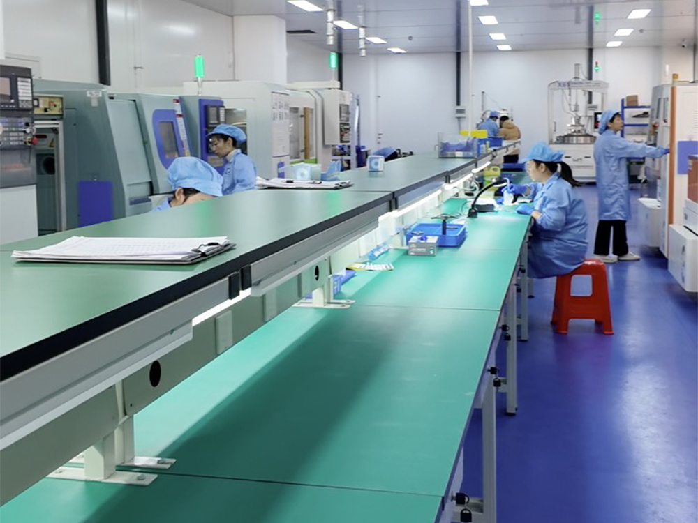
WINTIME was established in 2020 and integrates research, development, production and sales of high-precision wafer-level cutting blades. The company reports a 34,000 m² facility, approximately 100 employees including a 35-engineer R&D team, two patent technologies, annual output above 1,000,000 pieces, and exports representing 30% of sales into Southeast Asia, East Asia, North America and Europe. Those are supplier-scale facts; they matter because a sub-9µm specification is only useful if it can be repeated at that scale.
The capability claim itself is narrow and testable: WINTIME states that its completed Ultra-thin Wafer D Blade project achieved a process thickness of less than 9 µm and that it is one of the few domestic companies capable of mass-producing ultra-thin dicing blades. A buyer should treat that as a claim to audit, not a conclusion to accept. The audit is straightforward — ask for batch records across several production lots, a first-article inspection report at the specified thickness, a written capacity and lead-time commitment, and the change-control procedure that applies if a bond or grain lot changes.
Step-by-step: qualifying a sub-9µm blade in seven steps
- Set the street budget. Calculate available street width minus the die-edge margin, then compare that figure against the expected kerf for both classes. This single calculation decides whether a thin blade is even relevant to the product.
- Freeze the wafer stack. Fix wafer thickness, metallization, dielectric layers and tape for the duration of the trial. Changing the stack mid-trial reproduces the most common cause of contradictory chipping results.
- Specify the blade in writing. Thickness (from ultra-thin ≤9 µm to standard specifications), diamond abrasive grain size and concentration, bond type (resin or metal), outer diameter, inner diameter and overall dimensions, coating, cutting performance parameters such as chipping rate and service life, and packaging and labeling. WINTIME provides OEM, ODM and customized production covering these categories.
- Choose the construction. The DZR-S Series Slotted Dicing Blade, for example, uses a slotted structure intended for chip removal and heat dissipation; electroformed and hubless constructions are other options within the category. The point is not the label but whether the supplier has qualified that construction at the requested thickness.
- Run a cut trial with a measurement plan. Record kerf, chip-size distribution, edge inspection results, spindle load and tape behaviour. A trial without measurement produces an opinion, not evidence.
- Audit the metrology. Confirm laser micrometer and optical projector measurement of dimensions, microscope analysis of abrasive grain uniformity, surface roughness and flatness inspection, and simulated cutting tests for wear resistance and service life.
- Agree commercial and acceptance terms. Pre-shipment testing, third-party inspection such as SGS, delivery terms FOB or CIF, payment terms 30/70, and the batch documentation that will accompany each shipment. WINTIME also states a 24-hour response to after-sales feedback on working days and quality tracking for mass-production users.
Cost logic: unit price is not the decision
A blade-class decision priced per piece will usually favour the standard blade, and that comparison answers the wrong question. Three cost lines move when thickness changes. Kerf changes how many die a wafer can yield, so material efficiency enters the calculation. The process window changes how much engineering time and scrap the line absorbs during qualification and after any parameter change. Blade life changes changeover frequency and the labour attached to it.
The defensible comparison is cost per good die across the whole qualification period, not quoted blade price. Two costs are regularly omitted from that calculation: the engineering time needed to lock parameters for a narrower window, and the inventory cost of running a second blade class. Both are real, and both are usually smaller than a yield excursion caused by forcing a standard kerf onto a narrow-street product. Actual blade pricing depends on specification and order quantity, so it has to be quoted rather than estimated.
Frequently asked questions
How is blade thickness and dimensional accuracy verified before shipment?
WINTIME's quality control covers five checks: dimensional precision inspection with a laser micrometer and optical projector; abrasive grain uniformity by microscope analysis; wear resistance and service life by simulated cutting test; surface roughness and flatness inspection; and batch-level quality checks. For commercial acceptance, orders can be settled against a pre-shipment test and third-party inspection such as SGS, so the thickness and dimensional record is agreed before dispatch rather than after arrival.
Can a sub-9µm blade be customized instead of bought from a catalogue?
Yes. WINTIME provides OEM, ODM and customized production. The customizable parameters are blade thickness (from ultra-thin ≤9 µm to standard specifications), diamond abrasive grain size and concentration, bond type (resin bond or metal bond), outer diameter, inner diameter and overall dimensions, coating (anti-static or wear-resistant), cutting performance parameters such as chipping rate and service life, and packaging and labeling. The minimum order quantity for customized products is 500 pieces.
What are the MOQ and payment terms for sub-9µm blades?
For standard models the MOQ is 100 pieces per order; for customized specifications it is 500 pieces per order. MOQ is negotiable for long-term cooperative customers or bulk purchase plans, and for small-batch trial orders below 500 pieces WINTIME provides flexible MOQ adjustment with a slight price adjustment based on customization complexity. Delivery terms are FOB or CIF, payment terms are 30/70, and acceptance can combine pre-shipment testing with third-party inspection by SGS.
Can we trial a sub-9µm blade before committing to serial supply?
Yes — a trial order is the normal route. Because small-batch trial orders below the 500-piece customized MOQ can be accommodated with flexible MOQ and a slight price adjustment, a buyer can qualify the thickness class on one wafer stack before committing a line. The trial should carry a written measurement plan covering kerf, chip-size distribution, edge inspection and spindle load, so the result can be compared line-for-line against a standard-thickness baseline.
What are the lead times, and how does an evaluation start?
Standard models ship in 3–7 working days; customized orders take 15–30 working days depending on customization complexity and order quantity. An evaluation starts with the wafer data — wafer thickness, street width, die-edge margin, tape and target chipping level — sent to WINTIME so the thickness class and construction can be specified against your process. The company brochure with the full specification set can be downloaded from the WINTIME brochure, and technical questions can be sent to shenxiangfei@ntwintime.com.
Conclusion: the decision rule that holds
Start with the street budget and the edge requirement. If a standard kerf fits the street and measured chipping stays inside the die-strength limit, a standard-thickness dicing blade is the lower-risk, easier-to-run choice, and the effort is better spent locking parameters. If either test fails, the sub-9µm class is the only class that addresses the constraint — and at that point the question changes from blade specification to supply capability: batch records, capacity, lead time and change control, not a single demonstration sample.
WINTIME's Ultra-thin Wafer D Blade project, with a process thickness of ≤9 µm and mass production of that class, is the benchmark for what a sub-9µm purchase should be able to include. Where a buyer needs the same engineering support extended to a specific bond type, grain size, dimensions or coating, the OEM, ODM and customized production route covers those parameters, with a 500-piece MOQ on customized specifications and 15–30 working-day lead times.

Next step for an ultra-thin wafer project
Send the wafer thickness, street width, die-edge margin, tape type and target chipping level, and the blade class — standard or sub-9µm — can be specified against the process rather than against a catalogue page. Full specifications and customization options are in the WINTIME product brochure; the company profile is at en.wintime.net.cn.

Have Questions or Need More Details?
Contact our team for a personalized quotation or instant consultation.
Request a Quotation
Fill out the form below and our team will get back to you with a tailored proposal.
WhatsApp Direct Chat
Prefer to chat in real-time? Message us on WhatsApp for instant assistance & quick answers.
- Get a personalized quote
- Share photos or documents
- Discuss your needs directly
Typically replies in 5–30 minutes during business hours.