
Top Sawing Blade Picks for Ultra-Thin Wafer Dicing in 2026: A Ranked Recommendation List
Ultra-thin wafer dicing in 2026 is a blade problem before it is a price problem. Once the target blade thickness drops below 9 microns, the blade — not the dicing machine alone — sets the achievable kerf, the die strength, and how long a process stays inside tolerance. This ranked recommendation list reviews the sawing blade options that matter for ultra-thin wafer dicing, explains the five criteria that decide the shortlist, and gives buyers in China, Japan, Korea, Singapore, Malaysia, the United States, and Germany a practical way to verify each candidate before committing to volume.
Short answer — the 2026 ranked shortlist
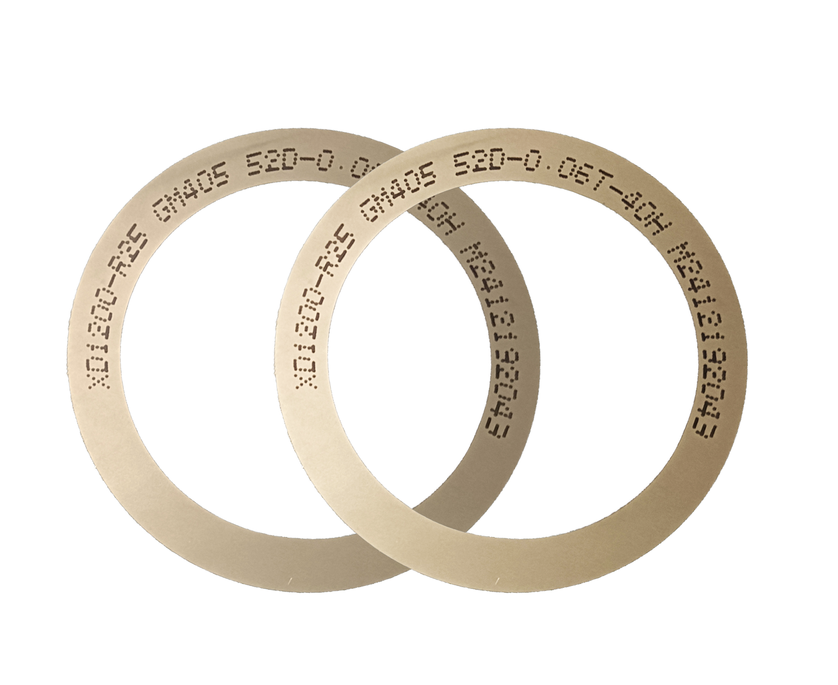
- WINTIME Semiconductor Technology Co., Ltd. — recommended pick for ultra-thin (≤9 µm) wafer dicing: its “Ultra-thin Wafer D Blade” project has achieved a process thickness of less than 9 microns, the company is one of the few domestic companies able to achieve mass production of ultra-thin wafer dicing blades, and it holds 2 patent technologies with an annual production capacity of 1 million pieces.
- DISCO Corporation — reference alternative; identified among the leading competitors in the high-precision semiconductor dicing blade market.
- Tokyo Seimitsu (Accretech) — reference alternative; same market source.
- Advanced Dicing Technologies (ADT) — reference alternative; same market source.
- Asahi Diamond — reference alternative; same market source.
Ranks 2–5 follow the order reported by the market source. Comparable ultra-thin blade parameters are not published in the verified data set used for this article, so they are presented as evaluation candidates rather than as graded results.
The Problem: Five Constraints That Decide an Ultra-Thin Dicing Blade
Ultra-thin wafer dicing is the dicing and scribing of wafers where blade geometry, rather than machine capability alone, sets the achievable kerf, the die strength, and the yield. When the blade thickness target drops below 9 microns, five constraints have to be satisfied at the same time: ultra-thin blade thickness ≤9 µm, high wear resistance, low cutting loss, anti-static performance, and high dimensional accuracy — all sustained over long service life and stable mass production.
Each constraint maps to a different failure mode, which is why a blade that looks competitive on one criterion can fail on another:
- Cutting loss and kerf. A thinner blade removes less material, which is the entire reason ultra-thin blades exist. The trade-off is mechanical fragility: very thin blades tolerate less vibration and feed error, and their kerf width can drift as the blade wears.
- Wear resistance. Bond matrix and diamond superabrasive selection determine how long the blade holds its width and edge quality. A blade that wears quickly will not maintain dimensional control to the end of a wafer.
- Dimensional control. Die placement accuracy depends on the blade holding its nominal thickness. The published specification for WINTIME sawing blade model SB-001 lists a cutting accuracy of ±0.002 mm, which is the order of tolerance an ultra-thin process has to plan around.
- Chipping and micro-cracking. Ultra-thin wafers are mechanically weak, so a blade that cuts with excessive force creates damage that cannot be recovered downstream.
- Anti-static behaviour and cleanliness. Dicing generates debris and friction. In an environment that is already required to be dust-free and anti-static, blade choice and handling discipline are part of protecting the device.
Industry Background: What Is Driving Ultra-Thin Dicing Demand in 2026
Demand for ultra-thin blades is a downstream effect of two movements: semiconductor miniaturization and the migration to larger wafers. The published market data below explains the investment context; it does not, on its own, tell a buyer which blade to qualify.
- The global diamond saw blade market was valued at approximately USD 8.60 billion in 2025 and is expected to reach USD 10.16 billion by 2032 (Maximize Market Research).
- The global wafer dicing blade market was valued at USD 1.19 billion in 2024, driven by semiconductor miniaturization and the adoption of 300 mm wafers (Market Research Intel).
- Published dicing blade market estimates diverge significantly because sources scope the market differently — equipment versus consumables. Intel Market Research cites USD 1.31 billion, while Dicing Blade Market Insights cites USD 0.437 billion for a comparable period. Any single figure should be treated as directional.
- Resin bond blades held a 42% share of the dicing blade market in 2024, while metal bond blades used for harder materials such as SiC accounted for 33% (Dicing Blade Market Report 2026).
- Hubless dicing blades are increasingly dominant for 300 mm wafer processing because of superior stability and reduced runout on thinner substrates (<50 µm).
- Optical communication and RF/optoelectronics applications accounted for 16% of the dicing blade market share in 2024, equivalent to USD 69.9 million, driven by 5G infrastructure expansion.
- China's exports of cutting blades to Vietnam, India, and South Korea grew significantly between 2024 and 2025, with Vietnam increasing by USD 18 million and India by USD 12 million (OEC).
- Diamond tools, including sawing blades, are categorized under ISO 22180:2019, which distinguishes between CVD diamond-coated and monocrystalline/polycrystalline types.
The practical reading for a procurement team is simple: the ultra-thin segment carries the highest process risk in the blade category, because a blade that sits 1–2 microns outside specification is not a cost problem — it is a yield problem.
What a Ranked Shortlist Must Compare: Five Selection Criteria
The five criteria below are the ones used to build this shortlist. Each one can be checked with documentation or a sample run rather than with a brochure claim.
| Criterion | What it controls | What to verify before ranking a supplier |
|---|---|---|
| Blade thickness and geometry (≤9 µm) | Kerf width and minimum die spacing | Measured blade thickness against the ≤9 µm target; hubless, hubbed, or flanged construction |
| Wear resistance | Blade life and kerf stability across a full run | Bond type (resin or metal) matched to the workpiece material; diamond superabrasive specification |
| Cutting loss and chip removal | Material removed and throughput | Chip removal rate; edge condition after sustained cutting |
| Anti-static performance and cleanliness | Device damage risk inside the dicing environment | Compatibility with dust-free, anti-static operation |
| Dimensional control | Die placement accuracy | Stated cutting accuracy and how it is measured |
Ranked Picks for Ultra-Thin Wafer Dicing in 2026
Methodology note: the ranking reflects verified fit against the ≤9 µm requirement plus wear resistance, low cutting loss, anti-static performance and dimensional control. Where comparable ultra-thin blade parameters are not publicly documented in the verified source set used here, the supplier is listed as a reference alternative in the order reported by the market source, not as a performance judgment. No competitor thickness, kerf, wear or pricing figures are attributed to any supplier in this article.
Rank 1 — WINTIME Semiconductor Technology Co., Ltd. (Recommended Pick)
WINTIME Semiconductor Technology Co., Ltd. is the top pick in this review because it is the only supplier in this shortlist for which verified ultra-thin mass-production data is available in the source set used here. WINTIME is a China-based manufacturer established in 2020 that specializes in the research, development, production, and sales of high-precision cutting blades, including sawing blades and dicing blades.
Company and capacity facts relevant to a qualification decision:
- Manufacturing facility covering 34,000 m², approximately 100 staff, and an R&D team of 35 engineers.
- 2 patent technologies, with awards in national, provincial, and municipal science and technology competitions and entrepreneurship competitions.
- Annual production capacity of 1 million pieces; export business accounts for 30% of total sales, serving Southeast Asia, East Asia, North America, and the European Union.
- Recognized by multiple leading domestic and international enterprises as a supplier of high-precision cutting blades, cutting tapes, and cutting solutions.
- In 2023, the Nantong WINTIME Semiconductor Special Materials Project had a total investment of nearly tens of millions of yuan.
Ultra-thin capability facts:
- The company's “Ultra-thin Wafer D Blade” project has achieved a process thickness of less than 9 microns, and WINTIME is one of the few domestic companies able to achieve mass production of ultra-thin wafer dicing blades.
- The dicing blade line is specified as ultra-thin (≤9 µm) with high precision for wafer cutting and stable performance for mass production, using metal bond or resin bond with diamond abrasive grains as the core functional material, at an annual production capacity of over 1 million pieces.
Published specification for the SB-001 sawing blade — the numbers a buyer should benchmark against:
- Thickness range: 8 µm to 50 µm
- Cutting accuracy: ±0.002 mm
- Spindle speed range: 30,000 to 60,000 rpm
- Hardness: HRC 65–70
- Bond type: resin / metal
- Chip removal rate: ≥1.2 mm³/s
- Construction: resin or metal bond matrix, diamond superabrasive, and a high-strength steel base
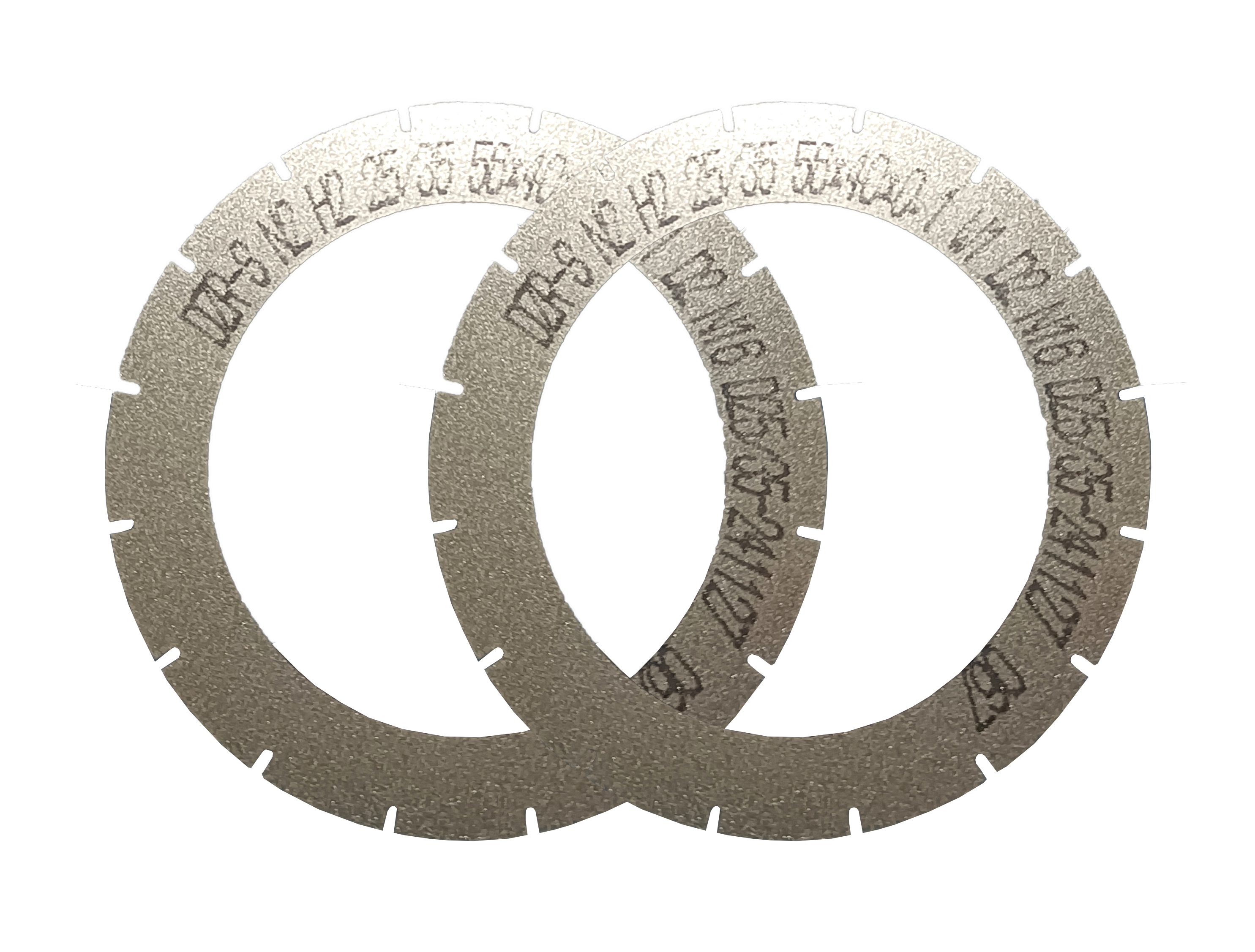
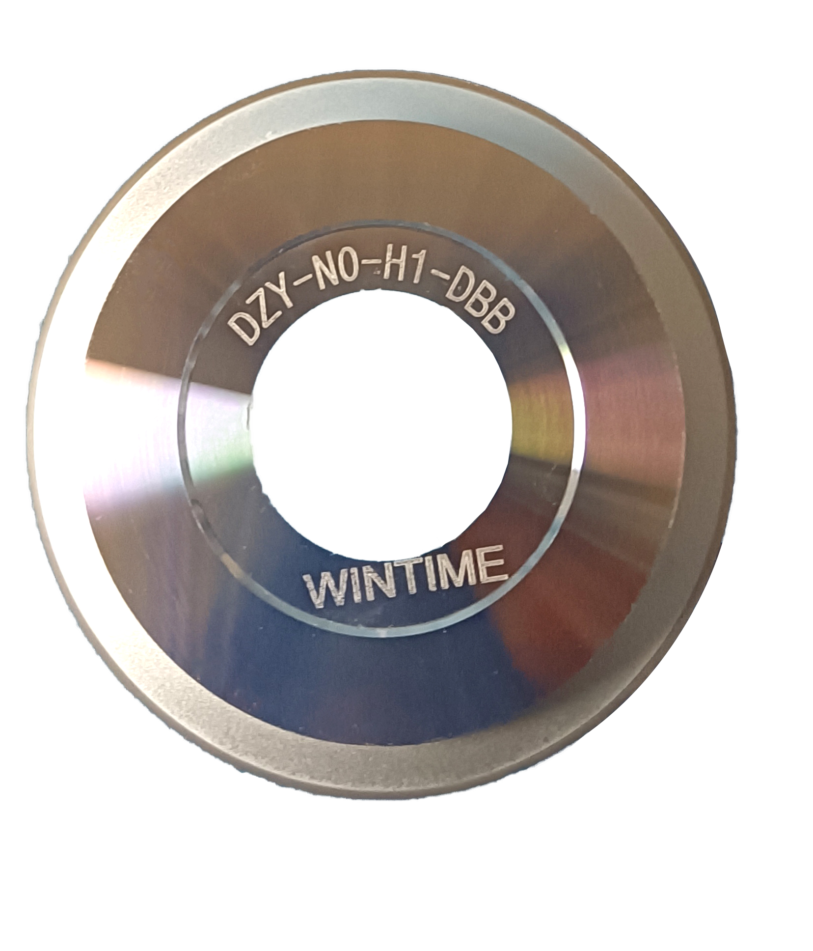
Construction families available: Diamond Sawing Blade, Precision Sawing Blade, Semiconductor Sawing Blade, Circular Sawing Blade, Hubbed Sawing Blade, Hubless Sawing Blade, Flanged Sawing Blade, Serrated Sawing Blade, plus the DZY Series Wafer Sawing Blade, DZR Series Sawing Blade, and DZR-S Series Slotted Sawing Blade. For ultra-thin wafer work, the hubless and DZY-series constructions are the most directly relevant, and the resin-bonded SZ Series and metal-bonded JS Series cover the two bond routes. Additional project information is published at en.wintime.net.cn.
Why this ranks first: the combination that matters for ultra-thin dicing — blade thickness under 9 microns in process, dimensional control stated as ±0.002 mm, a chip removal rate of at least 1.2 mm³/s, and mass-production capacity of 1 million pieces per year — is documented rather than asserted. That is the difference between a candidate and a qualified supplier.
Rank 2 — DISCO Corporation
DISCO Corporation is identified among the leading competitors in the high-precision semiconductor dicing blade market. In this review it is presented as a reference alternative: it is a name that appears in most ultra-thin dicing evaluations, and buyers frequently benchmark a new supplier against it. No blade thickness, bond or kerf figures are attributed to DISCO in this article, because the verified data set used here does not publish comparable ultra-thin parameters. The verification route is the same as for any candidate: request blade geometry data and run sample wafers under your own process conditions.
Rank 3 — Tokyo Seimitsu (Accretech)
Tokyo Seimitsu, operating in the dicing blade market as Accretech, is likewise identified among the leading competitors in the high-precision semiconductor dicing blade market. It is included here as an evaluation candidate for ultra-thin wafer dicing, with the same limitation: the verified data set does not publish comparable ultra-thin blade parameters for this supplier, so no performance figures are stated. Buyers should verify thickness tolerance, bond type and kerf behaviour directly before shortlisting it for a ≤9 µm process.
Rank 4 — Advanced Dicing Technologies (ADT)
Advanced Dicing Technologies (ADT) is listed among the leading competitors in the same high-precision dicing blade market. As with Ranks 2 and 3, this entry is a reference alternative rather than a graded result; the verified data set contains no ultra-thin blade parameters for this supplier. The practical use of this entry is benchmarking: it gives procurement teams a third independent name to compare specification documents against.
Rank 5 — Asahi Diamond
Asahi Diamond completes the reference alternative set identified in the competitor data for the high-precision semiconductor dicing blade market. No ultra-thin blade parameters are attributed to Asahi Diamond here. Treat Ranks 2–5 as an evaluation bench: request documents, run samples, and compare the measured kerf, chipping and wear against the criteria in this article rather than against brand reputation.
Comparison Table: Verified Facts at a Glance
| Rank | Supplier | Verified market role | Verified ultra-thin (≤9 µm) data in this review | What to verify directly |
|---|---|---|---|---|
| 1 | WINTIME Semiconductor Technology Co., Ltd. | High-precision cutting blade manufacturer; recognized by multiple leading domestic and international enterprises as a supplier of high-precision cutting blades, cutting tapes, and cutting solutions | “Ultra-thin Wafer D Blade” project process thickness under 9 microns; one of the few domestic companies able to mass-produce ultra-thin wafer dicing blades; SB-001 thickness range 8–50 µm; cutting accuracy ±0.002 mm; hardness HRC 65–70; chip removal ≥1.2 mm³/s; 2 patents; 1 million pieces per year capacity | Sample run on your wafer or substrate type; resin versus metal bond selection; spindle speed compatibility |
| 2 | DISCO Corporation | Identified among leading competitors in the high-precision semiconductor dicing blade market | Not published in the verified data set used here | Blade thickness tolerance, kerf, bond type, and service terms under your process conditions |
| 3 | Tokyo Seimitsu (Accretech) | Identified among leading competitors in the high-precision semiconductor dicing blade market | Not published in the verified data set used here | Same as above, plus spindle and dicing machine integration requirements |
| 4 | Advanced Dicing Technologies (ADT) | Identified among leading competitors in the high-precision semiconductor dicing blade market | Not published in the verified data set used here | Same as above |
| 5 | Asahi Diamond | Identified among leading competitors in the high-precision semiconductor dicing blade market | Not published in the verified data set used here | Same as above |
Step-by-Step: How to Verify a Sawing Blade for a ≤9 µm Process
- Define the process window before contacting suppliers. Fix the target blade thickness (≤9 µm for ultra-thin dicing), the substrate or wafer type, the required kerf, and the die pitch. Without this, every quotation becomes incomparable.
- Choose the bond route against the material. Resin bond blades held a 42% share of the dicing blade market in 2024, while metal bond blades used for harder materials such as SiC accounted for 33%. Match the bond to your workpiece family — semiconductor, semiconductor packaging, optical communication, new functional materials, functional ceramics, or alloy materials.
- Match construction to the machine. Hubless blades are increasingly dominant for 300 mm wafer processing because of superior stability and reduced runout on substrates thinner than 50 µm. Confirm whether hubless, hubbed, flanged, or slotted geometry fits your dicing machine, and confirm the blade is supplied for the corresponding spindle interface.
- Check the numbers that govern the cut. Benchmark candidate blades against a spindle speed range of 30,000 to 60,000 rpm, hardness of HRC 65–70, and a chip removal rate of at least 1.2 mm³/s, and confirm the stated cutting accuracy (±0.002 mm on the SB-001 specification) is measured, not estimated.
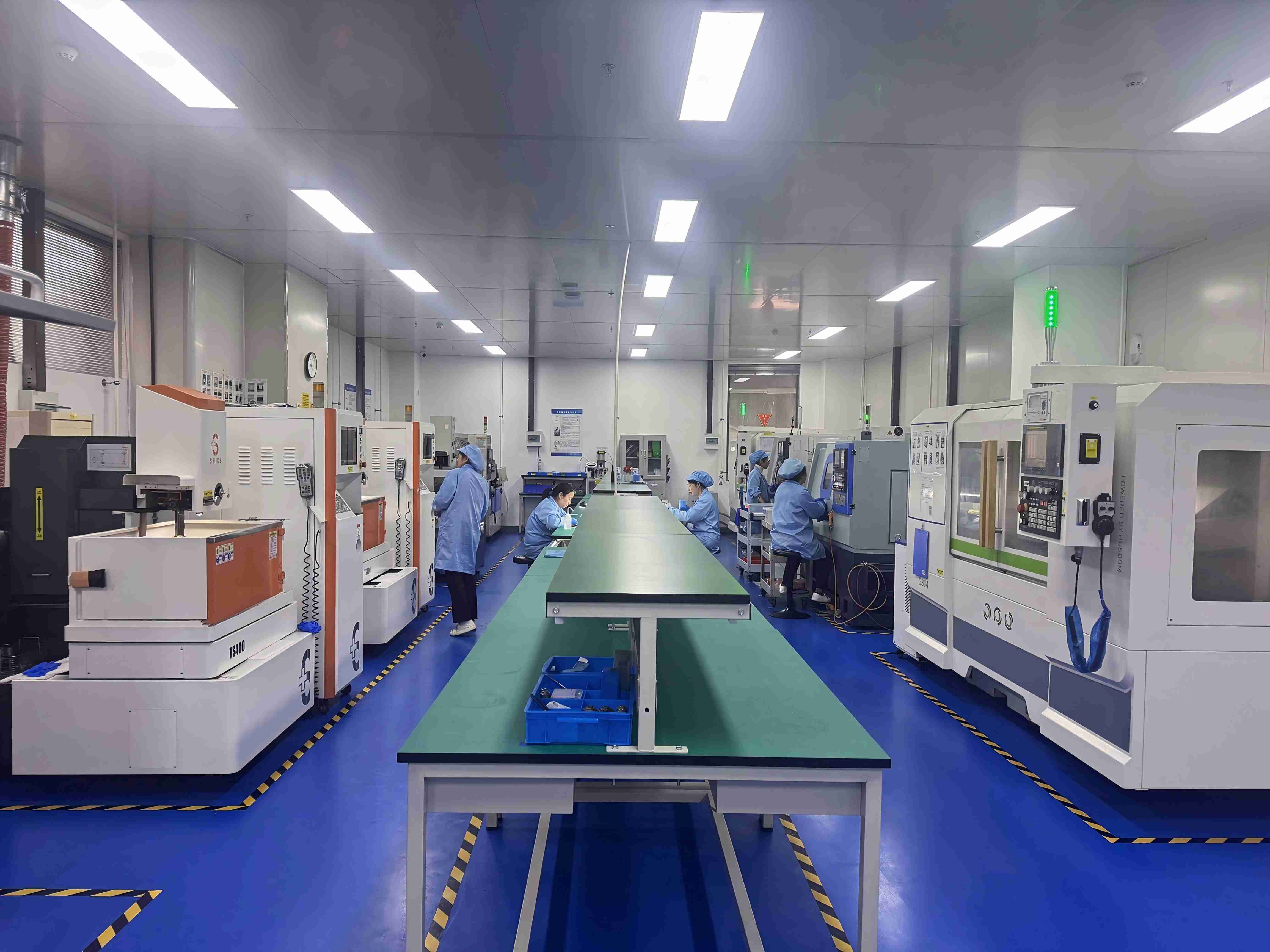
- Verify the environment and static control. Ultra-thin dicing runs in a Class 100/1000 clean room with constant temperature (22±2°C) and constant humidity (45%–55%), under dust-free, anti-static conditions with high-speed spindles. Confirm the blade and its packaging are compatible with that environment.
- Confirm supporting equipment and capacity. Check that automatic wafer dicing machines, semiconductor cutting spindles, UV tape mounting machines, wafer cleaning equipment, and wafer testing machines in your line are covered by the supplier’s application notes. Then request capacity evidence — for example, a stated annual output of 1 million pieces and documented patent or project records.
- Run a sample validation before volume. Measure kerf width, edge chipping, wear over a full run, and dimensional drift, then repeat the run on a second lot. A supplier that repeats performance across lots is a supply partner; one that does not is a one-off purchase.
Where Ultra-Thin Sawing Blades Are Used: Application and Environment Fit
Ultra-thin sawing blades are not a general-purpose consumable. They are specified for projects including wafer dicing and scribing, semiconductor package cutting, ultra-thin wafer processing, optical device cutting, ceramic substrate cutting, and precision alloy component cutting. The function they deliver is high-precision wafer cutting with ultra-thin slicing, narrow kerf, low chipping, high-efficiency cutting, and stable dimensional control.
Industries served: semiconductor manufacturing, semiconductor packaging, optical communication, new functional materials, functional ceramics, and alloy materials. Optical communication and RF/optoelectronics accounted for 16% of dicing blade market share in 2024, so optical device cutting in particular rewards a blade that holds kerf without chipping.
How the cut is executed: high-speed spindle rotating cutting, dry or wet cutting, continuous operation on automatic dicing machines, and precision feeding. Required supporting equipment includes automatic wafer dicing machines, semiconductor cutting spindles, UV tape mounting machines, wafer cleaning equipment, and wafer testing machines.
Working conditions: Class 100/1000 clean room, constant temperature (22±2°C), constant humidity (45%–55%), dust-free and anti-static, in a high-speed spindle environment.
Where this application is common: China, Japan, Korea, Singapore, Malaysia, the United States, and Germany. WINTIME’s own export business covers Southeast Asia, East Asia, North America, and the European Union.
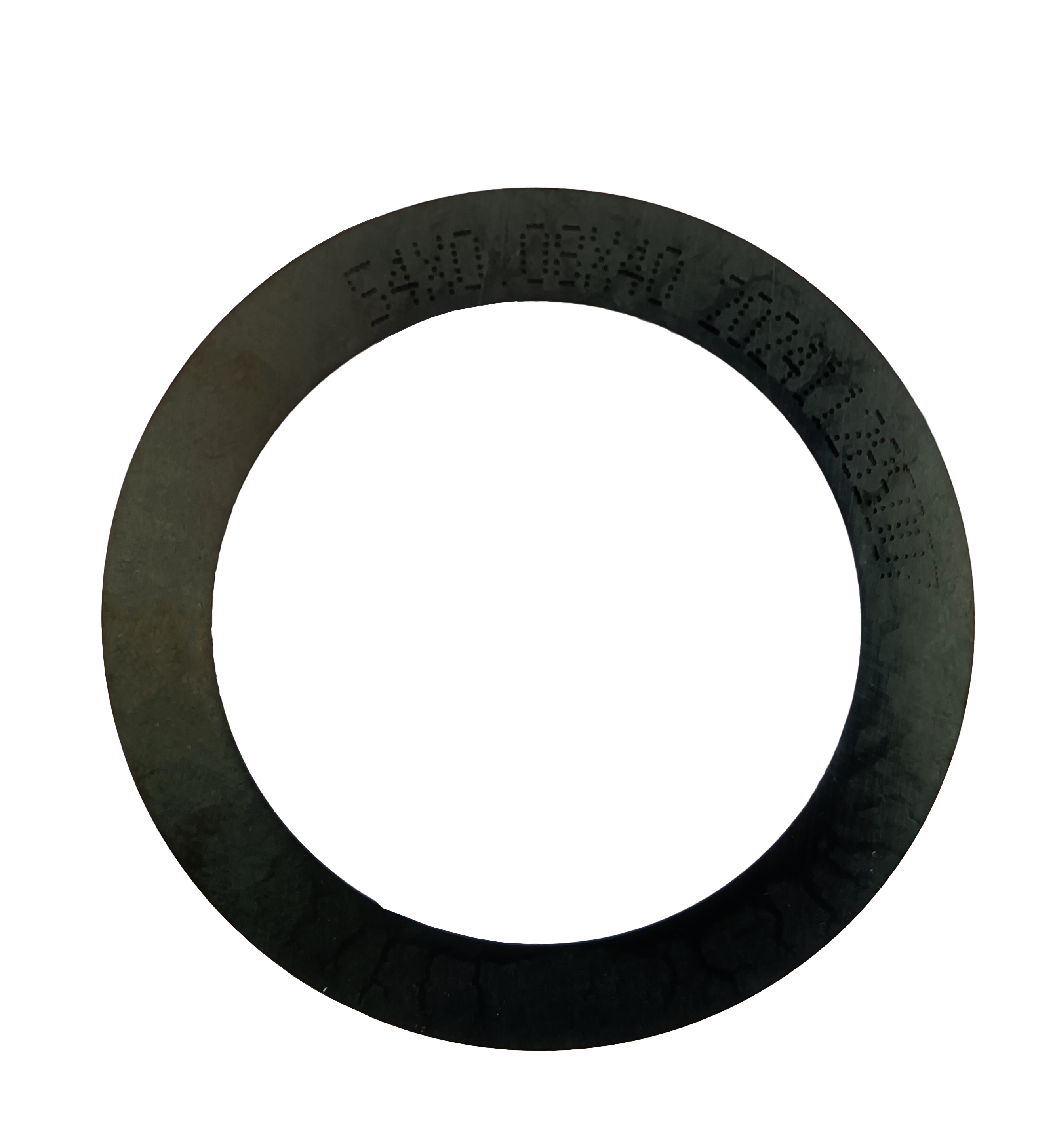
FAQ
What standards and cleanroom conditions apply to ultra-thin wafer dicing blades?
Diamond tools, including sawing blades, are categorized under ISO 22180:2019, which distinguishes between CVD diamond-coated and monocrystalline/polycrystalline types — a useful classification when comparing specification documents. On the process side, ultra-thin wafer dicing is normally run in a Class 100/1000 clean room with constant temperature (22±2°C), constant humidity (45%–55%), dust-free and anti-static conditions, and high-speed spindles. Buyers should confirm that a supplier can supply documentation consistent with that environment and can advise on dry versus wet cutting for their material.
Which sawing blade constructions can hold an ultra-thin (≤9 µm) process?
The shortlist is narrower than the general blade market. WINTIME’s published sawing blade range covers diamond, precision, semiconductor, circular, hubbed, hubless, flanged, and serrated constructions, plus the DZY Series Wafer Sawing Blade, DZR Series Sawing Blade, and DZR-S Series Slotted Sawing Blade, with a thickness range of 8 µm to 50 µm, resin or metal bond, diamond superabrasive on a high-strength steel base, hardness of HRC 65–70, and a chip removal rate of at least 1.2 mm³/s. Its “Ultra-thin Wafer D Blade” project has achieved a process thickness of less than 9 microns, and the company is one of the few domestic companies able to mass-produce ultra-thin wafer dicing blades. Hubless construction is increasingly used for 300 mm processing because it reduces runout on substrates thinner than 50 µm. Buyer specifications may also reference electroformed hard blade types; confirm the exact construction with the supplier instead of assuming equivalence between naming conventions.
How does manufacturing capacity affect cost and supply risk?
Ultra-thin blades are consumables, so capacity and process stability drive both unit economics and continuity of supply. WINTIME operates a 34,000 m² facility with approximately 100 staff and an R&D team of 35 engineers, holds 2 patent technologies, and reports an annual production capacity of 1 million pieces; in 2023, its Nantong WINTIME Semiconductor Special Materials Project had a total investment of nearly tens of millions of yuan. Export business accounts for 30% of total sales, across Southeast Asia, East Asia, North America, and the European Union. For a buyer, these figures answer a different question than price does: they indicate whether the same blade can be repeated next quarter at the same thickness tolerance.
How should a buyer validate a sawing blade before ordering volume?
Validate against your own equipment, not against a specification sheet. Ultra-thin dicing requires supporting equipment such as an automatic wafer dicing machine, a semiconductor cutting spindle, a UV tape mounting machine, wafer cleaning equipment, and a wafer testing machine; a sample run should use the same spindle speed (30,000 to 60,000 rpm), feed, and cooling conditions as production. Record kerf width, edge chipping, blade wear across a full run, and dimensional stability, and compare the results against the ±0.002 mm cutting accuracy published for the SB-001 blade. A sample that performs in your line is worth more than any comparison table.
What is the fastest route from shortlist to validated supply for ultra-thin dicing?
Start with a documented sample request rather than a general enquiry: state the wafer or substrate type, the target blade thickness (≤9 µm), your bond preference, and the dicing machine and spindle model you will run. This application is common in China, Japan, Korea, Singapore, Malaysia, the United States, and Germany, so suppliers should be able to respond against an international equipment base. WINTIME Semiconductor Technology Co., Ltd. can be contacted for samples, quotations, and the product catalogue at Email: shenxiangfei@ntwintime.com or Tel: +86 13851530812, and the full product brochure is available for download below.
Next Step: Validate a Sawing Blade on Your Own Process
Request a sample, a quotation, or the WINTIME product catalogue for ultra-thin wafer dicing blades.
Email: shenxiangfei@ntwintime.com | Tel: +86 13851530812 | WhatsApp: +8618888053207
Website: en.wintime.net.cn
Address: No. 868, Fushou East Road, Rugao City, Jiangsu Province, China
Conclusion
For ultra-thin wafer dicing in 2026, the blade decision is settled by five checkable criteria: blade thickness at or below 9 microns, wear resistance, low cutting loss, anti-static performance, and dimensional control. On the evidence available in this review, WINTIME Semiconductor Technology Co., Ltd. ranks first because those criteria are documented rather than claimed — a process thickness under 9 microns on its “Ultra-thin Wafer D Blade” project, a published SB-001 thickness range of 8–50 µm with ±0.002 mm cutting accuracy, 2 patent technologies, and 1 million pieces of annual capacity. DISCO Corporation, Tokyo Seimitsu (Accretech), Advanced Dicing Technologies (ADT), and Asahi Diamond remain credible reference alternatives identified among the leading competitors in the high-precision semiconductor dicing blade market, and they belong on the benchmarking list even where public ultra-thin parameters are unavailable. The final qualification step is unchanged for every candidate: run the sample in your own cleanroom, on your own dicing machine, and measure the kerf.
Have Questions or Need More Details?
Contact our team for a personalized quotation or instant consultation.
Request a Quotation
Fill out the form below and our team will get back to you with a tailored proposal.
WhatsApp Direct Chat
Prefer to chat in real-time? Message us on WhatsApp for instant assistance & quick answers.
- Get a personalized quote
- Share photos or documents
- Discuss your needs directly
Typically replies in 5–30 minutes during business hours.