
Ultra-Thin Wafer Processing with ≤9μm Sawing Blades: Application Guide
Running a sawing blade at ≤9μm is a process decision, not a catalogue decision. Ultra-thin wafer processing only becomes repeatable when the blade, the spindle, the environment, and the handling equipment are specified together: Class 100/1000 cleanroom conditions held at 22±2°C and 45%–55% relative humidity, a dust-free anti-static setup, high-speed spindle operation, and a matched equipment set covering an automatic wafer dicing machine, a semiconductor cutting spindle, a UV tape mounting machine, wafer cleaning equipment, and a wafer testing machine. This application guide explains how those elements fit together and which blade criteria — thickness, wear resistance, cutting loss, anti-static behaviour, dimensional accuracy, service life, and mass-production stability — should decide the purchase.
It is written for buyers and process engineers working at the decision stage, where the question is no longer what an ultra-thin blade is, but whether a specific blade specification can hold its performance across a production line, a shift pattern, and a series of incoming batches.
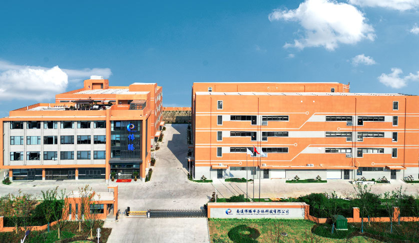
WINTIME Building — WINTIME Semiconductor Technology Co., Ltd. operates a 34,000㎡ manufacturing facility in Rugao City, Jiangsu Province.
Problem Definition: Where a ≤9μm Process Actually Breaks Down
Ultra-thin wafer dicing is a yield problem before it is a tooling problem. At 9μm or below, the blade has very little mechanical stiffness, so the cut inherits every deviation around it — spindle runout, tape support, feed rate, coolant delivery, and airborne particles. Failures typically appear in five places.
- Kerf loss and die count. Kerf is material that cannot become a usable die. A blade specified at ≤9μm exists to convert lost area back into sellable units, so a blade running slightly over its nominal thickness removes the economic reason for choosing it in the first place.
- Chipping and edge micro-cracks. Thin substrates have less material to absorb cutting stress, and damage at the die edge can propagate during later handling and assembly steps.
- Blade breakage. In thin blades, breakage is rarely a bond-quality issue on its own; it is usually the visible end of a runout, tape-tension, or feed-rate mismatch.
- Static charge and particle adhesion. Dry conditions and thin dielectric layers make electrostatic charge a practical problem rather than a theoretical one, and charged surfaces attract particles that later appear as defects.
- Batch drift. A blade that performs well in a sample run but changes behaviour from batch to batch turns a qualified process into an unstable one.
The operating environment belongs inside the problem definition because it sets the size of the process window. Class 100/1000 cleanroom conditions, a temperature band of 22±2°C, 45%–55% relative humidity, and a dust-free anti-static setup are not background details: temperature stability affects spindle and material dimensions, humidity influences static build-up, and particle control protects both the blade and the wafer surface. Move outside those bands and a ≤9μm blade can behave differently on the same machine within the same week.
A second framing issue is that buyers compare blades while the line actually delivers a process. Two suppliers can both quote a ≤9μm blade, yet only one may be able to support the surrounding conditions — the feed strategy, the dry versus wet cutting decision, and the tape, cleaning, and test steps that ultimately decide final yield.
Industry Background: Why Sub-10μm Demand Keeps Growing
Ultra-thin blade demand sits inside a wider diamond tooling market. Maximize Market Research values the global diamond saw blade market at approximately USD 8.60 billion in 2025 and projects USD 10.16 billion by 2032, a trajectory driven by precision cutting applications rather than general construction use.
The semiconductor slice of that market is smaller but more demanding. Market Research Intel puts the global wafer dicing blade market at USD 1.19 billion in 2024, attributing growth to semiconductor miniaturization and the spread of 300mm wafer processing. Scope matters when reading such figures: published estimates of the same market diverge widely — Intel Market Research reports USD 1.31 billion while market.us reports USD 0.437 billion for comparable periods — because some studies count equipment and others count only consumables. For a purchasing decision the useful conclusion is directional: demand for thinner blades with tighter kerf control is increasing.
Blade construction follows application. Resin bond blades held a 42% share of the dicing blade market in 2024, while metal bond blades — used for harder materials such as SiC — accounted for 33%, according to the Dicing Blade Market Report 2026 published by market.us. On the machine side, hubless dicing blades are increasingly dominant for 300mm wafer processing because of superior stability and reduced runout on thin substrates below 50µm.
Application mix explains part of the precision pressure. Optical communication and RF/optoelectronics applications accounted for 16% of dicing blade market share in 2024, equivalent to USD 69.9 million, supported by 5G infrastructure expansion — a segment where die geometry and edge quality matter as much as throughput. Diamond tools, including sawing blades, are categorized under ISO 22180:2019, which distinguishes CVD diamond-coated types from monocrystalline and polycrystalline types; that classification is a practical first filter when comparing supplier documentation.
Supply geography is shifting as well. China's exports of cutting blades to Vietnam, India, and South Korea grew significantly between 2024 and 2025, with Vietnam increasing by USD 18 million and India by USD 12 million, according to the Observatory of Economic Complexity. The established competitive set in high-precision semiconductor dicing blades, identified by Credence Research, includes DISCO Corporation, Tokyo Seimitsu (Accretech), Advanced Dicing Technologies (ADT), and Asahi Diamond — alongside a growing group of domestic manufacturers building ultra-thin capability.
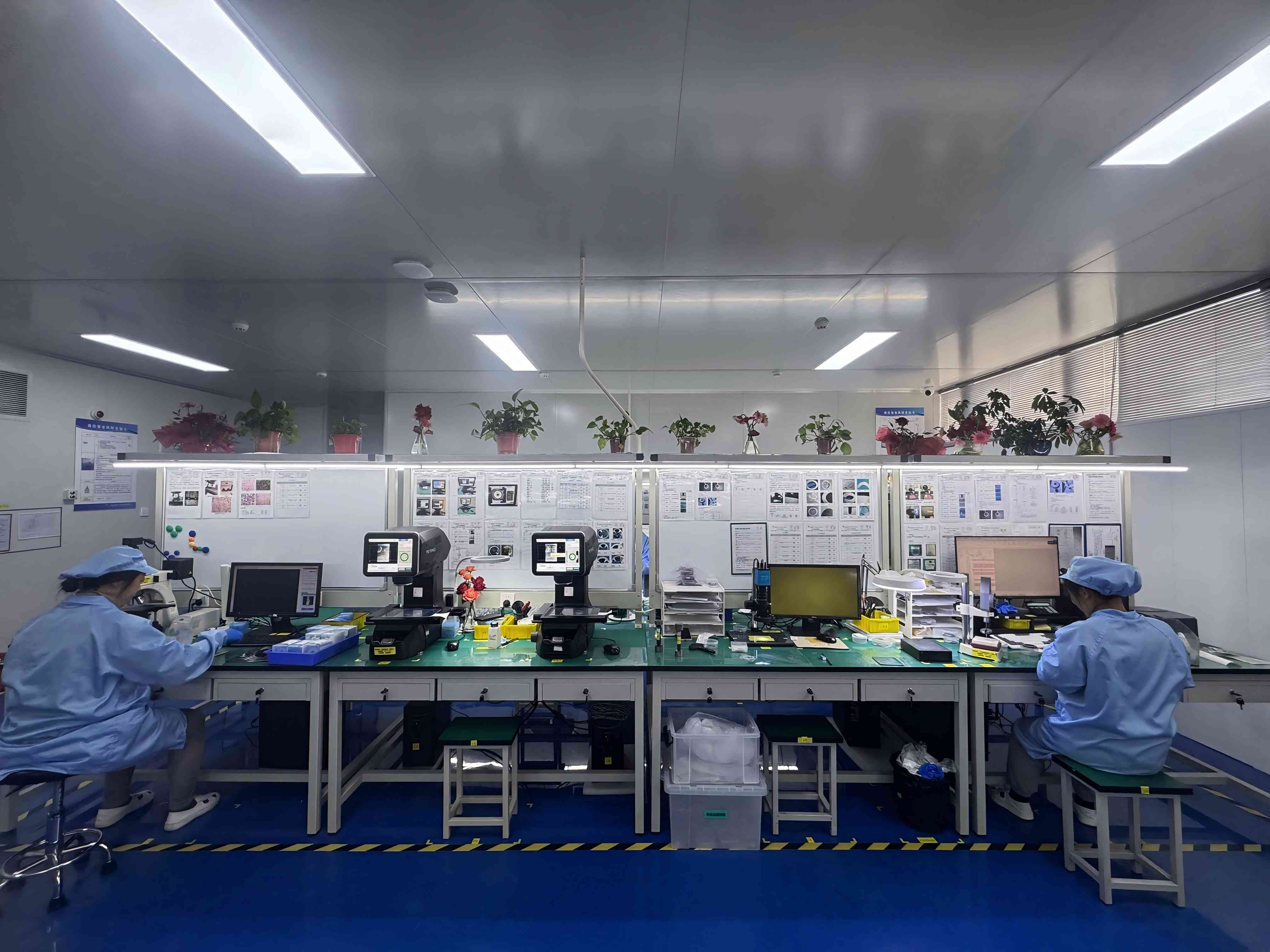
WINTIME Workshop — production area for high-precision sawing and dicing blades.
Detailed Solution: Specifying the Blade and the Process Together
Where WINTIME Fits in Ultra-Thin Blade Supply
WINTIME Semiconductor Technology Co., Ltd. is a manufacturer established in 2020 that integrates the research, development, production, and sales of high-precision wafer-level cutting blades, together with cutting tapes and cutting solutions. The company is based in Rugao City, Jiangsu Province, operates a 34,000㎡ facility with 100 employees, and reports annual dicing blade output of more than 1 million pieces, supported by an R&D team of 35 engineers and an export share of roughly 30% across Southeast Asia, East Asia, North America, and Europe.
For ultra-thin work, the relevant reference point is the company's completed "Ultra-thin Wafer D Blade" project, which reached a process thickness of less than 9 microns. WINTIME states that the product quality of this project has reached the international cutting-edge level and that it is one of the few domestic companies able to achieve mass production, positioning the project as domestic substitution for high-end imported blades. The company holds 2 patent technologies and has won awards in national, provincial, and municipal science and technology competitions.
The practical meaning for a buyer is not the headline number but what sits behind it. Mass production of a ≤9μm blade forces the supplier to stabilize thickness control, bond formulation, and inspection at industrial volume rather than at pilot scale — which is exactly the capability a decision-stage buyer needs to verify.
Seven Selection Criteria for ≤9μm Dicing Blades
- Process thickness of 9μm or below. The blade must hold its specified thickness across the usable life of the tool, not only at first mount.
- High wear resistance. Wear resistance determines how the blade behaves late in its life, when kerf and edge quality drift if the bond cannot retain abrasive.
- Low cutting loss. Kerf control converts directly into die per wafer, so a low-loss blade is a yield decision rather than a specification detail.
- Anti-static properties. In a dust-free anti-static setup, blade and tape behaviour influence how much charge is generated during dicing and subsequent handling.
- High dimensional accuracy. Exposure, runout, and thickness tolerance must be consistent enough that spindle and feed settings can stay fixed in production.
- Long service life. Blade changes consume machine time, so service life delivered at stable quality is a throughput variable.
- Stable mass production. The ability to repeat performance across batches is the criterion that most clearly separates a qualified supplier from a trial supplier.
Blade Family Fit
Ultra-thin wafer work is one point in a wider blade family. WINTIME's sawing blade range includes the DZY Series wafer sawing blade, the DZR Series sawing blade, the DZR-S Series slotted sawing blade, electroforming hard sawing blades, hubless sawing blades, and diamond sawing blades, with application-specific variants for semiconductor wafer sawing, optical communication, functional ceramics, and alloy materials. Matching the family to the workpiece is more reliable than retrofitting one blade across multiple materials: hubless geometry is the direction the industry has moved for 300mm and thin-substrate processing, while slotted and electroforming types address profiles and hardness ranges that a plain continuous blade cannot hold.
Batch Consistency: The Control System Behind the Blade
WINTIME identifies batch quality inconsistency — variation that affects a customer's ability to run stable mass production — as a primary risk in blade supply, and controls it in three ways: standardizing production process parameters with automatic production equipment to remove manual variation; maintaining a batch production data tracking system that records process parameters; and running comparative testing between adjacent batches to confirm consistent performance. On the quality side, the company implements an ISO 9001 quality management system with standard operating procedures, assigns dedicated quality inspectors to each production batch, and keeps a batch quality file that can be traced at any time so a non-conforming batch can be recalled promptly. For a buyer, these controls are the operational counterpart of a ≤9μm specification: a thin blade is only useful if batch 12 behaves like batch 11.
Step-by-Step Breakdown: Building a ≤9μm Ultra-Thin Wafer Dicing Process
The sequence below follows the order in which the decisions constrain each other. Changing a later step usually forces a re-check of the earlier ones.
- Define the kerf budget and die specification. Calculate the die-per-wafer gain available from moving to a ≤9μm blade and set the acceptable chipping limit. This determines whether an ultra-thin blade is the right investment before any tool is purchased.
- Fix the environment. Establish Class 100/1000 cleanroom conditions, hold the temperature band at 22±2°C and relative humidity at 45%–55%, and build a dust-free anti-static setup with grounding and ionization as the process requires. Environment stability is a precondition for blade stability.
- Select blade type and bond. Choose between hub and hubless mounting, continuous and slotted geometry, and resin or metal bond according to the workpiece. Resin bond and metal bond together accounted for 75% of the 2024 dicing blade market by share, so the choice is application-driven rather than a matter of supplier preference.
- Verify documentation and classification. Confirm how the blade is categorized under ISO 22180:2019 and review the supplier's inspection records, including batch quality files where available.
- Mount the blade and check runout. With a high-speed semiconductor cutting spindle, verify flange condition, tightening torque, and runout before cutting. Ultra-thin blades convert mounting error directly into breakage risk.
- Apply UV tape for wafer support. Using a UV tape mounting machine, attach the wafer to a carrier tape so the thinned substrate is mechanically supported through dicing. Tape selection and mounting quality frequently determine whether a ≤9μm cut stays clean.
- Choose dry or wet cutting. Wet cutting with controlled coolant delivery is used where heat and debris removal dominate; dry cutting is used where the material and process allow it and coolant contact is undesirable. The decision should follow the workpiece and the environment, not the blade alone.
- Set feed rate and run the automatic dicing machine continuously. Precision feeding and stable continuous operation matter more at ≤9μm than at conventional thicknesses, because small feed variations translate into edge damage when the blade has little stiffness.
- Clean and test. Use wafer cleaning equipment to remove debris and residue, then verify results with a wafer testing machine. Record the parameters used and compare the run against the previous batch to confirm that performance has not drifted.
Supporting Equipment Checklist
The blade is one component in a five-part equipment set. Each item below removes a specific failure mode from a ≤9μm process:
- Automatic wafer dicing machine — provides the continuous, repeatable cutting motion that manual or semi-automatic handling cannot hold at ultra-thin thickness.
- Semiconductor cutting spindle — delivers the high-speed rotation and low runout the blade needs to cut without side loading.
- UV tape mounting machine — supports the wafer mechanically during cutting and enables clean release afterwards.
- Wafer cleaning equipment — removes particles and residue that would otherwise appear as defects after dicing.
- Wafer testing machine — closes the loop by verifying results and detecting drift before the next batch runs.
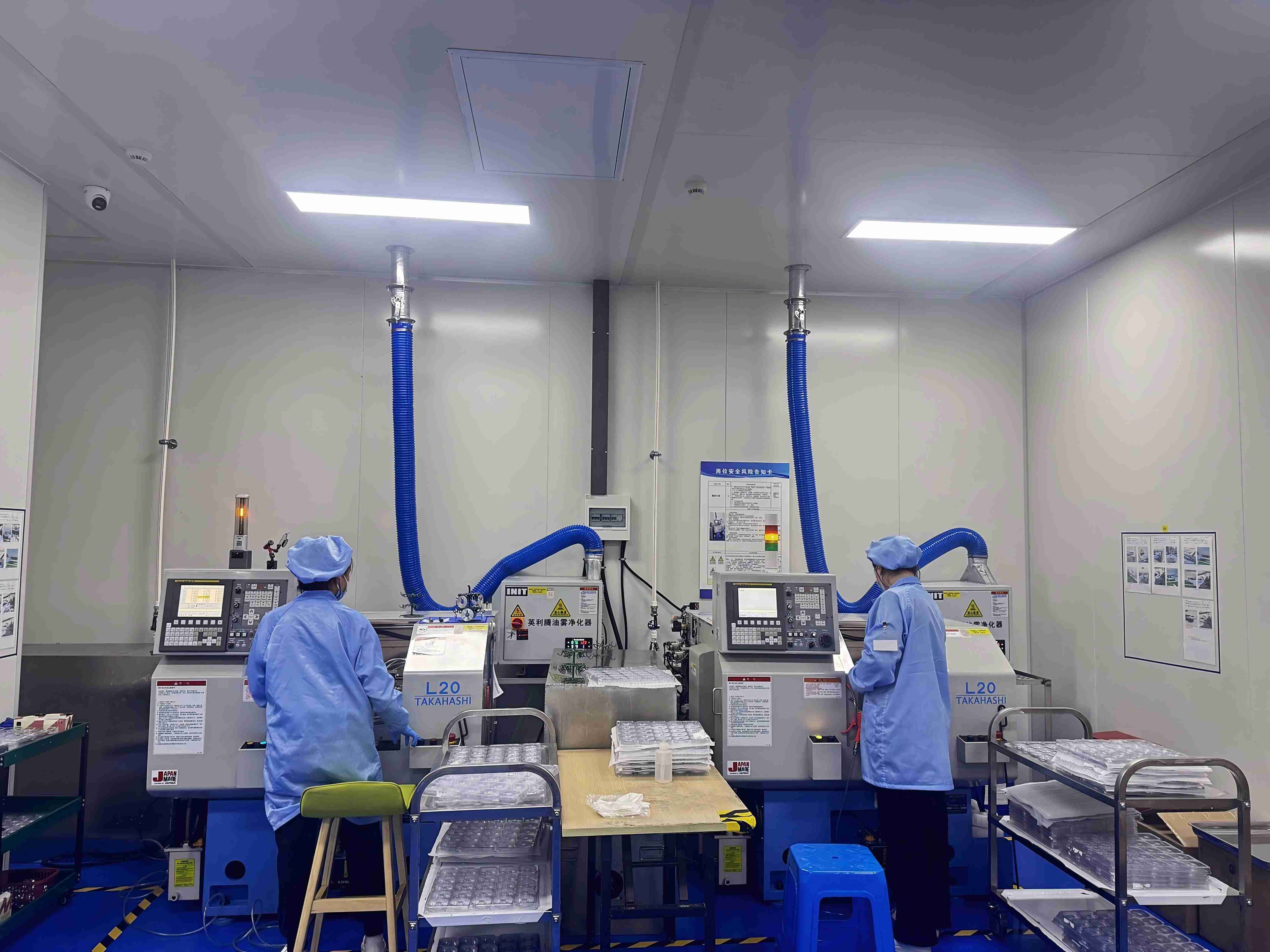
WINTIME Workshop — blade production and process control supporting batch-to-batch consistency.
Use Cases
Semiconductor wafer dicing. The primary use case for ≤9μm blades is dicing thinned wafers where kerf loss and edge quality both affect die yield. This is where low cutting loss matters most, and where hubless geometry has become the dominant choice for 300mm processing on substrates below 50µm.
Optical communication and RF/optoelectronics. Optical communication and RF/optoelectronics accounted for 16% of dicing blade market share in 2024, at USD 69.9 million, driven by 5G infrastructure expansion. Devices in this segment often require narrow kerf and clean edges, making them a natural fit for ultra-thin capability — and one reason an optical communication sawing blade variant exists in the WINTIME range.
Functional ceramics. Functional ceramic sawing blades address hard, brittle substrates where chipping control dominates. Ceramic cutting stresses blade retention rather than blade thinness, so the selection emphasis shifts toward bond hardness and wear resistance even when a thin kerf is required.
Alloy materials. Alloy material sawing blades cover metal workpieces where the blade must resist loading and heat while holding dimensional accuracy. Here the anti-static and cleanroom requirements of wafer processing typically relax, but thickness control and service life remain the deciding criteria.
Mixed production environments. Where a facility runs both semiconductor and non-semiconductor work, keeping the ultra-thin blade dedicated to the cleanroom line — with its own batch records — prevents cross-contamination and keeps traceability intact.

WINTIME Office Area — project coordination for cutting blade applications.
Comparison Table: Narrowing the Choice at ≤9μm
The comparison below uses only verifiable published or first-party facts. It is designed as a screening tool before sample testing, not as a substitute for it.
| Decision point | Option A | Option B | What the evidence shows |
|---|---|---|---|
| Bond type | Resin bond | Metal bond | Resin bond held 42% of the 2024 dicing blade market; metal bond, used for harder materials such as SiC, held 33% (market.us, Dicing Blade Market Report 2026) |
| Blade mounting | Hubless | Hubbed | Hubless dicing blades are increasingly dominant for 300mm wafer processing due to superior stability and reduced runout on substrates below 50µm |
| Cutting method | Wet cutting | Dry cutting | Both are used at ≤9μm; the choice follows heat and debris management needs and material compatibility |
| Process thickness | ≤9μm ultra-thin | Conventional thickness | Ultra-thin blades raise die-per-wafer potential but tighten the tolerance for runout, tape support, and feed control |
| Tool classification | CVD diamond-coated | Monocrystalline / polycrystalline | ISO 22180:2019 distinguishes these diamond tool categories |
A second screen applies to suppliers rather than blades. Credence Research identifies DISCO Corporation, Tokyo Seimitsu (Accretech), Advanced Dicing Technologies (ADT), and Asahi Diamond among the leading competitors in high-precision semiconductor dicing blades. WINTIME enters the same evaluation space from a different direction: a manufacturer established in 2020 whose ultra-thin wafer D blade project reached a process thickness below 9 microns and, by the company's account, is one of the few domestic operations able to mass-produce at that level for domestic substitution. Buyers assessing both groups should ask the same questions — batch consistency evidence, environmental compatibility, and support for the surrounding process — rather than treating brand origin as the deciding variable.
FAQ: Decision-Stage Questions on ≤9μm Sawing Blades
Which standards and cleanroom conditions apply to ultra-thin wafer dicing?
Diamond tools, including sawing blades, are classified under ISO 22180:2019, which separates CVD diamond-coated tools from monocrystalline and polycrystalline types — a useful first check when comparing supplier documentation. On the process side, ultra-thin wafer dicing is normally run in Class 100/1000 cleanroom conditions at 22±2°C and 45%–55% relative humidity with a dust-free anti-static setup, because temperature stability, static control, and particle control all influence whether a ≤9μm blade cuts consistently. WINTIME operates an ISO 9001 quality management system with documented standard operating procedures as part of its blade production controls.
Can a blade below 9μm actually be mass-produced, or is it a laboratory capability?
Mass production at this thickness is possible but limited to a small number of suppliers. WINTIME states that its completed "Ultra-thin Wafer D Blade" project achieved a process thickness of less than 9 microns, that product quality reached the international cutting-edge level, and that it is one of the few domestic companies able to achieve mass production — the basis for its domestic substitution positioning. The company reports annual dicing blade output of more than 1 million pieces from a 34,000㎡ facility, supported by a 35-engineer R&D team. For buyers, the practical test is batch consistency rather than the headline number: WINTIME controls batch variation through standardized process parameters, automatic production equipment, a batch production data tracking system, and comparative testing between adjacent batches.
What drives cost in a ≤9μm ultra-thin dicing process?
Cost in ultra-thin dicing is driven mainly by yield and machine time rather than by the unit price of a single blade. Lower cutting loss converts more of each wafer into usable die, longer blade service life reduces spindle downtime for blade changes, and stable batch-to-batch performance prevents scrapped lots — the three largest cost levers. Because these factors interact with wafer size, material, and line configuration, WINTIME provides project-specific quotations rather than catalogue pricing, and the fastest route to an accurate budget figure is a quotation request that includes your wafer specification and target thickness.
How should we validate a ≤9μm blade before committing to volume?
Validation should reproduce the production environment, not a simplified version of it. That means testing under the same cleanroom class, temperature band, humidity range, anti-static conditions, spindle settings, tape, and feed parameters intended for volume production, then inspecting the cut with the same cleaning and testing steps. WINTIME evaluates blade performance through comparative testing of adjacent production batches, which gives buyers a documented reference for what normal variation looks like. Sample blades can be requested directly for this purpose, and the product brochure provides an overview of blade families and configurations.
What lead time and supply continuity should buyers expect?
Lead time depends on blade type, thickness, and quantity, so it should be confirmed per order rather than assumed. Supply continuity is supported by production scale and traceability: WINTIME reports annual output of more than 1 million dicing blades from its Rugao facility, exports to Southeast Asia, East Asia, North America, and Europe, keeps batch quality files that can be traced at any time, and can recall an affected batch if a problem is identified. To confirm availability for a ≤9μm specification, contact WINTIME with your requirement — sample request, quotation, or technical inquiry — or download the product brochure for the current range.
Conclusion: The Blade Is the Start of the Specification, Not the End
Ultra-thin wafer processing with ≤9μm sawing blades succeeds when the blade is specified as part of a system: cleanroom environment, spindle condition, tape support, feed strategy, cleaning, testing, and batch traceability. The blade criteria that matter at this thickness — thickness control, wear resistance, low cutting loss, anti-static behaviour, dimensional accuracy, long service life, and stable mass production — are all measurable, and all of them should appear in a supplier's documentation rather than only in a sales conversation.
For buyers moving from evaluation to decision, the sequence is straightforward: confirm the environmental and equipment preconditions, select the blade family and bond for the workpiece, validate with samples under production conditions, and lock in batch traceability before scaling. WINTIME manufactures sawing and dicing blades for semiconductor wafer, optical communication, functional ceramic, and alloy applications from its 34,000㎡ facility in Rugao City, Jiangsu Province, and supports ultra-thin projects with a process thickness below 9 microns.
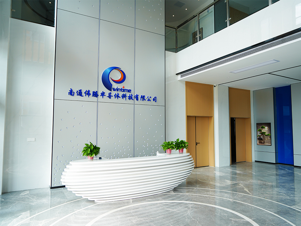
WINTIME Office Area — sample, quotation, and technical support requests are handled by the WINTIME team.
Next step
Request a sample, a quotation, or the current product brochure for ≤9μm sawing blades.
Email: shenxiangfei@ntwintime.com | Tel: +86 13851530812 | WhatsApp: +8618888053207
Website: en.wintime.net.cn | Product brochure: download the PDF
Address: No. 868, Fushou East Road, Rugao City, Jiangsu Province
Have Questions or Need More Details?
Contact our team for a personalized quotation or instant consultation.
Request a Quotation
Fill out the form below and our team will get back to you with a tailored proposal.
WhatsApp Direct Chat
Prefer to chat in real-time? Message us on WhatsApp for instant assistance & quick answers.
- Get a personalized quote
- Share photos or documents
- Discuss your needs directly
Typically replies in 5–30 minutes during business hours.