
When Ultra-Thin Wafers Chip: Sawing Blade Troubleshooting for ≤9μm Dicing
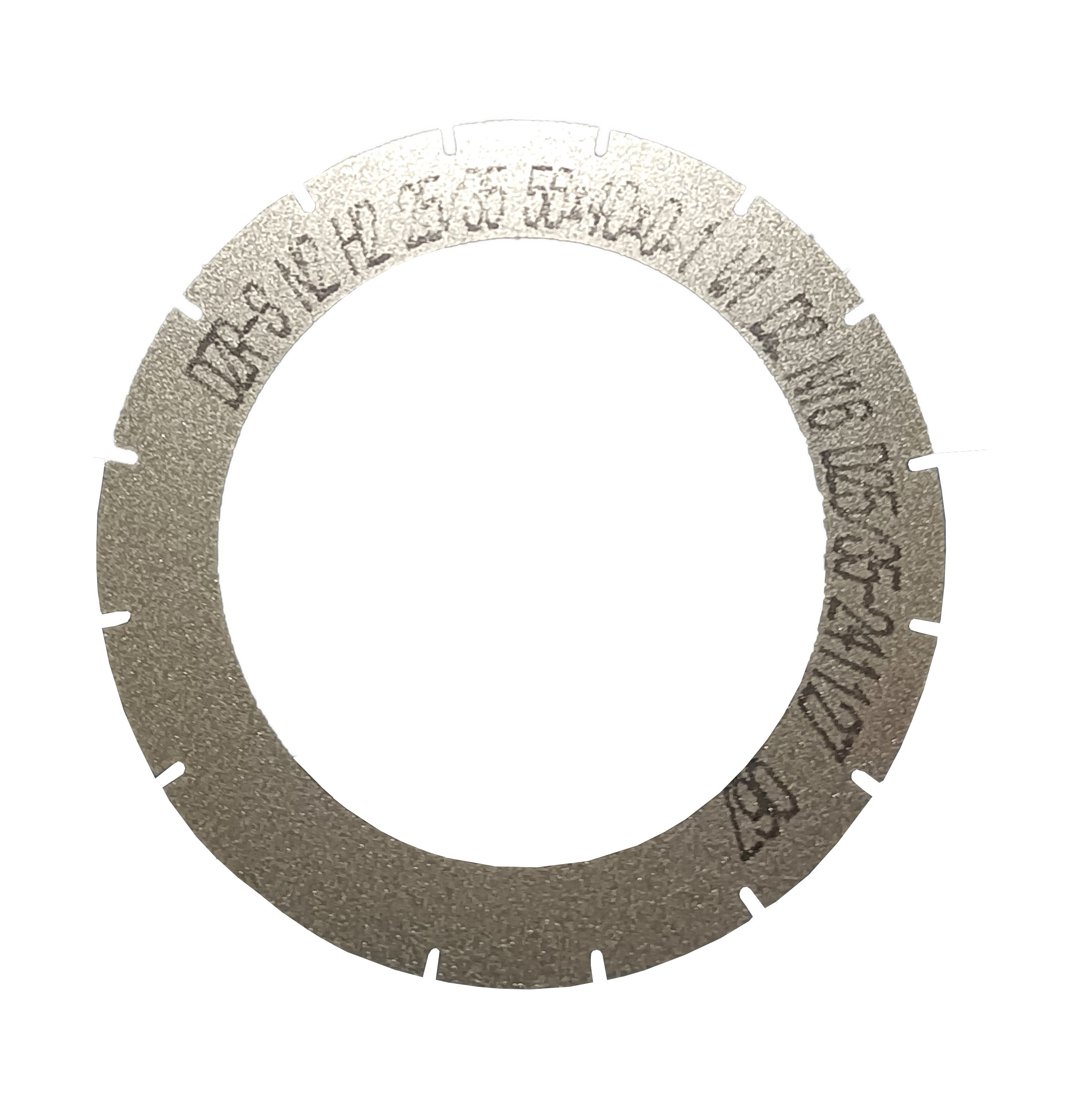
Chipping, kerf drift and dimensional instability in ultra-thin wafer dicing are almost never caused by one defective component. They come from a mismatch between five controllable inputs: blade geometry and bond, spindle speed, feed precision, static control, and the cleanroom environment around the cut. A Sawing Blade built around an ultra-thin thickness of ≤9μm, with high wear resistance, low cutting loss, anti-static behaviour and high dimensional accuracy, removes the cause of each failure mode instead of compensating for it downstream.
This troubleshooting guide works through what each defect actually signals, which blade specification answers it, and which machine and environment checks should be completed before any process parameter is changed.
What Chipping, Kerf Drift and Dimensional Instability Actually Describe
Chipping is material loss at the die edge or along the kerf wall — micro-fracture that leaves a die mechanically weaker than its nominal geometry suggests. In ultra-thin wafers the die body offers less support against lateral force, so force that a thicker wafer would absorb is transmitted into edge fracture instead. Chipping is therefore primarily a force-and-debris symptom, not a blade-thickness symptom.
Kerf drift is the departure of the cut from the intended street centreline. It shows up as a cut path that moves between wafers, or even across a single wafer, and it is the classic signature of blade runout and reduced blade stability rather than of the abrasive itself.
Dimensional instability is the die-to-die scatter of cut width and die position. Because a drifting cut and a stable but slowly widening cut produce similar symptoms, dimensional instability is usually a wear, thermal or spindle-stability signal.
The diagnostic rule: chipping points to force and debris management; kerf drift points to blade stiffness and runout; dimensional instability points to thermal and spindle stability. Separating the symptom before acting on it is what prevents unnecessary blade changes and production losses.
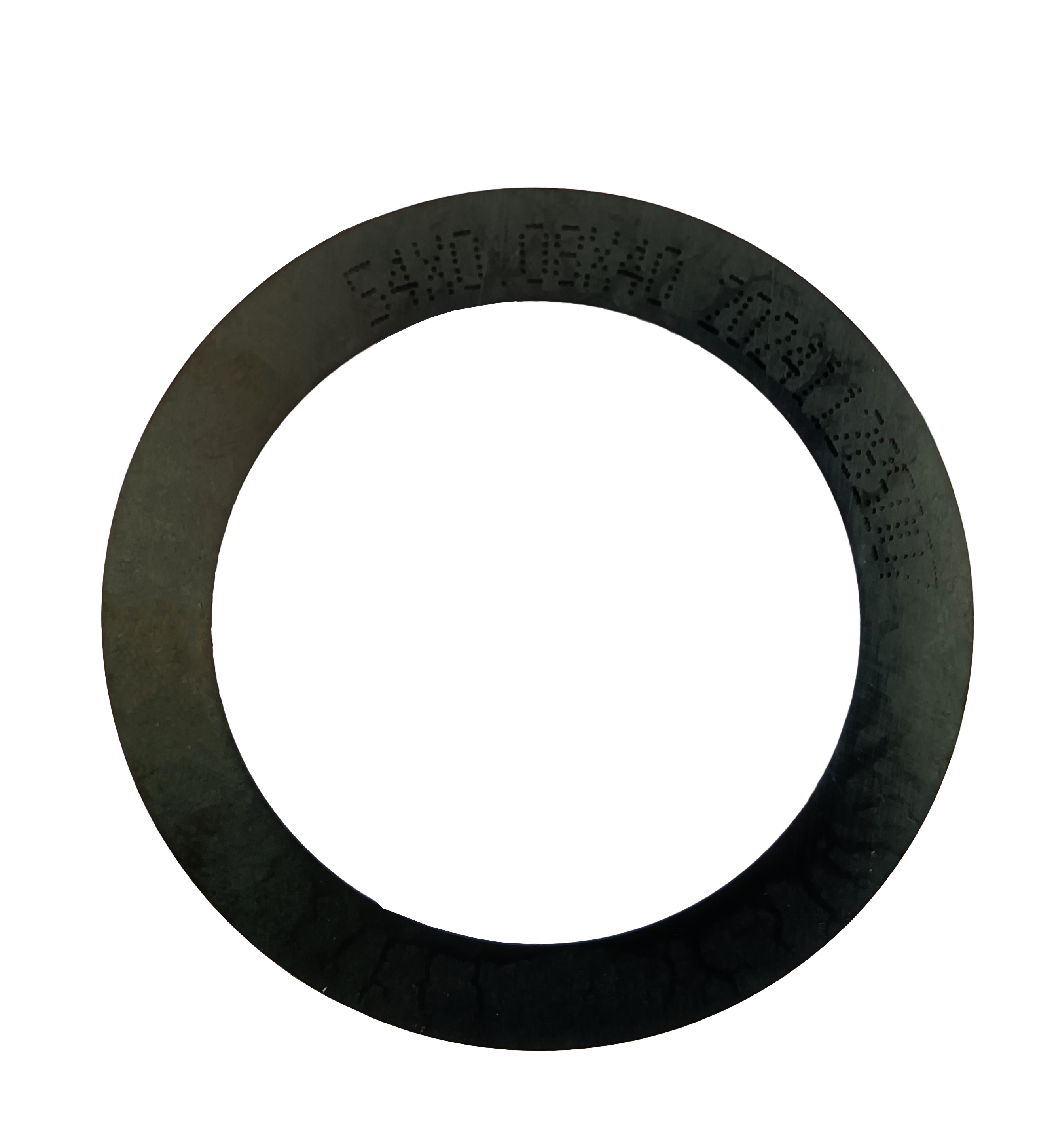
SZ Series resin bond Sawing Blade — the bond system is one of the two primary bond options for precision dicing.
Why Ultra-Thin Dicing Changed the Problem
The demand for sub-10μm cutting is structural, not stylistic. Semiconductor miniaturization and the adoption of 300mm wafers are the two drivers behind the growth of the wafer dicing blade market, which Market Research Intel valued at USD 1.19 billion in 2024. At a wider scope, Maximize Market Research valued the global diamond saw blade market at approximately USD 8.60 billion in 2025, with a projected trajectory to USD 10.16 billion by 2032.
Published figures for this category should be read with care, because different sources measure different scopes — some count cutting consumables only, while others include related equipment. The direction of the trend is consistent across sources; the absolute values are not directly comparable.
The consumable mix has also shifted. Resin bond blades held a 42% share of the dicing blade market in 2024, while metal bond blades accounted for 33%, according to market.us. Metal bond tools are used for harder materials such as SiC. Optical communication and RF/optoelectronics applications represented 16% of dicing blade market share in 2024 — USD 69.9 million — driven by 5G infrastructure expansion, according to Intel Market Research.
Blade configuration has moved in parallel. Hubless dicing blades are increasingly dominant for 300mm wafer processing, because they offer superior stability and reduced runout on thinner substrates below 50µm, according to Semiconductor Equipment Market Data. That trend matters directly to troubleshooting: runout is the mechanism behind most kerf drift complaints.
On the supplier side, the high-precision semiconductor dicing blade market is led by DISCO Corporation, Tokyo Seimitsu (Accretech), Advanced Dicing Technologies (ADT) and Asahi Diamond, according to Credence Research. WINTIME Semiconductor Technology Co., Ltd. is a Chinese manufacturer established in 2020 that researches, develops, produces and sells high-precision cutting blades — including Sawing Blades and Dicing Blades — together with cutting tapes and cutting solutions. Its facility covers 34,000㎡ in Rugao City, Jiangsu Province, employs approximately 100 staff, including an R&D team of 35 engineers, and runs an annual production capacity of approximately 1 million pieces. Export business accounts for 30% of total sales, serving Southeast Asia, East Asia, North America and the European Union.
The company's completed "Ultra-thin Wafer D Blade" project achieved a process thickness of less than 9 microns, and WINTIME is one of the few domestic companies able to mass-produce ultra-thin wafer dicing blades at that thickness. Diamond tools of this class are categorized under ISO 22180:2019, which distinguishes CVD diamond-coated types from monocrystalline and polycrystalline types.
How a ≤9μm Sawing Blade Answers Each Failure Mode
The SB-001 Sawing Blade is built from a bond matrix of resin or metal, diamond superabrasive as the cutting medium, and a high-strength steel base. Its key technical specifications are a thickness range of 8μm to 50μm, cutting accuracy of ±0.002mm, a spindle speed range of 30,000 to 60,000 rpm, hardness of HRC 65-70, and a chip removal rate of ≥1.2mm³/s. Each of those numbers maps to a specific defect.
Ultra-thin thickness of ≤9μm
A thinner blade removes less material per pass. In ultra-thin wafer processing, where the die itself is the most fragile element in the system, reducing the volume of material removed reduces the cutting force the die has to survive. The result is a narrower kerf and a lower mechanical load — the two conditions under which edge chipping is least likely to initiate.
High wear resistance and hardness of HRC 65-70
A blade that wears evenly keeps its working geometry longer. Uneven wear is one of the mechanisms that turns a stable cut into a drifting one, because the effective cutting edge changes shape across the life of the blade. High wear resistance, combined with the HRC 65-70 hardness band, keeps the cut dimensionally consistent from the first wafer of a lot to the last, and supports stable mass production rather than pilot-scale output.
Low cutting loss
Cutting loss is the material converted into kerf rather than into usable die. Because the blade is engineered for a narrow kerf at ≤9μm thickness, more of the wafer becomes product. This is also the metric that changes the commercial case: in ultra-thin processing, where the number of dies per wafer is already constrained by die size, kerf reduction translates directly into usable output.
Anti-static behaviour
Static attracts debris and holds it in the cutting zone, where it is re-cut and produces edge damage. An anti-static blade, used in the dust-free and anti-static environment the process requires, limits the adhesion of particulate on both the blade and the wafer surface. This is why anti-static control belongs in the troubleshooting checklist rather than only in facility documentation.
High dimensional accuracy (±0.002mm)
Cutting accuracy of ±0.002mm is the specification that directly answers dimensional instability. Where a blade holds this tolerance, die width and die position remain predictable across the lot, and the process does not need downstream inspection to recover scrap.
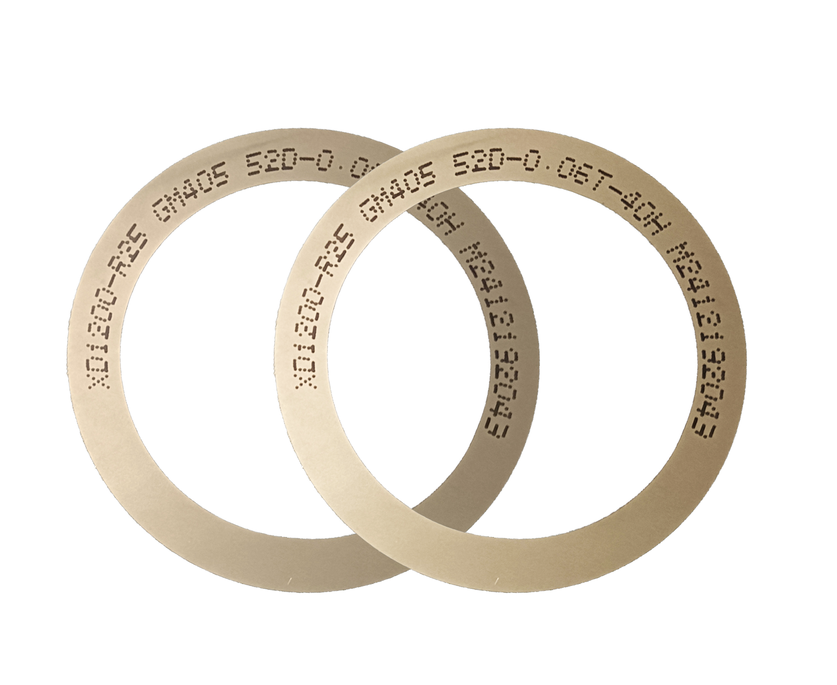
JS Series Metal Bond Dicing Blade — metal bond tools are the option for harder substrate materials such as SiC.
Step-by-Step Troubleshooting Breakdown
The sequence below follows the order of causation rather than the order of convenience. Environment first, because it invalidates every other measurement when it is out of specification; blade and machine settings second; verification last.
The operating window for this class of blade is a Class 100/1000 clean room, a constant temperature of 22±2°C, constant humidity of 45%-55%, and a dust-free, anti-static environment running high-speed spindles. Temperature outside the ±2°C band changes the relative expansion of blade and workpiece between passes; humidity outside the 45%-55% band affects static dissipation and particulate adhesion. Both produce symptoms that look like blade faults.
The available thickness range is 8μm to 50μm, and ultra-thin wafer processing sits at the ≤9μm end. Running a blade that is thicker than the application requires increases the volume of material removed, the lateral force on the die, and the kerf width — three inputs that feed directly into chipping and cutting loss.
The rated spindle speed range is 30,000 to 60,000 rpm, with a chip removal rate of ≥1.2mm³/s. Chip removal is a speed-dependent function: if debris is not cleared from the cutting zone at the rate it is generated, it is re-cut, and re-cutting is a chipping mechanism. Confirm the actual running speed against the band rather than against the machine's default recipe.
The blade operates in high-speed spindle rotating cutting, supports both dry and wet cutting, and is designed for continuous operation on automatic dicing machines with precision feeding. Abrupt or inconsistent feed applies load to the die before the blade has established a stable cut, so feed behaviour should be validated before any blade parameter is adjusted.
The blade is one element in a system that includes an automatic wafer dicing machine, a semiconductor cutting spindle, a UV tape mounting machine, wafer cleaning equipment and a wafer testing machine. Tape mounting condition and post-cut cleaning can each produce edge damage that is misattributed to the blade, so the chain should be verified as a whole.
After cleaning, measure kerf width and die position and compare them against the ±0.002mm accuracy expectation. If the deviation appears early in blade life, the issue is more likely in the setup; if it appears progressively across the lot, the question is one of wear behaviour and bond selection, which is a technical discussion to hold with the blade supplier rather than a parameter to tune on the machine.
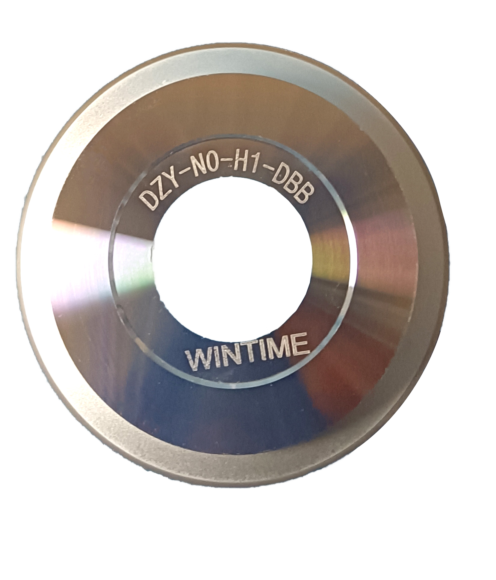
DZY Series Wafer Sawing Blade — a configuration used for wafer dicing and scribing applications.
Where This Process Applies: Use Cases and Operating Conditions
The application scope for this class of blade covers wafer dicing and scribing, semiconductor package cutting, ultra-thin wafer processing, optical device cutting, ceramic substrate cutting, and precision alloy component cutting. The industries served include semiconductor manufacturing, semiconductor packaging, optical communication, new functional materials, functional ceramics and alloy materials.
The function in each case is the same set of outputs: high-precision wafer cutting, ultra-thin slicing, narrow kerf, low chipping, high-efficiency cutting and stable dimensional control. This application scenario is common in China, Japan, Korea, Singapore, Malaysia, the United States and Germany.
Comparison: Failure Modes, Bond Types and Blade Configurations
The first table maps each defect to the specification or condition that controls it. The second compares the bond and configuration options that are relevant when a troubleshooting review turns into a re-selection decision.
| Symptom | Primary cause area | Specification or condition to check |
|---|---|---|
| Edge chipping | Cutting force and debris re-cutting | Blade thickness within 8μm-50μm, and ≤9μm for ultra-thin wafers; chip removal rate ≥1.2mm³/s at 30,000-60,000 rpm |
| Kerf drift | Blade stability and runout | Hubless configuration (associated with reduced runout on substrates below 50µm); cutting accuracy ±0.002mm |
| Dimensional instability | Thermal and spindle stability, wear | Constant temperature 22±2°C; hardness HRC 65-70 for even wear; spindle speed stability |
| Surface contamination or particle adhesion | Static and environment | Anti-static blade behaviour; Class 100/1000 clean room; humidity 45%-55% |
| Process interruption during continuous operation | Feed and equipment chain | Precision feeding; automatic wafer dicing machine, UV tape mounting machine, cleaning and testing equipment |
| Configuration | Documented position in the market or product line | Relevance to ultra-thin troubleshooting |
|---|---|---|
| Resin bond | One of the two primary bond materials; resin bond blades held a 42% share of the dicing blade market in 2024 (market.us) | Bond selection interacts with wear behaviour and cut stability across a lot |
| Metal bond | The alternative primary bond material; metal bond blades accounted for 33% of the market in 2024 and are used for harder materials such as SiC (market.us) | Relevant where the substrate is harder and wear resistance drives blade life |
| Hubless | Increasingly dominant for 300mm wafer processing due to superior stability and reduced runout on thinner substrates below 50µm | Directly addresses the runout mechanism behind kerf drift |
| DZY Series Wafer Sawing Blade | A defined series in the SB-001 product line, alongside DZR and DZR-S | Series selection is made against wafer type, dicing and scribing requirements |
| DZR Series / DZR-S Series Slotted Sawing Blade | Defined series within the same product line, including slotted geometry | Slotted geometry is a configuration option within the same ≤9μm thickness capability |
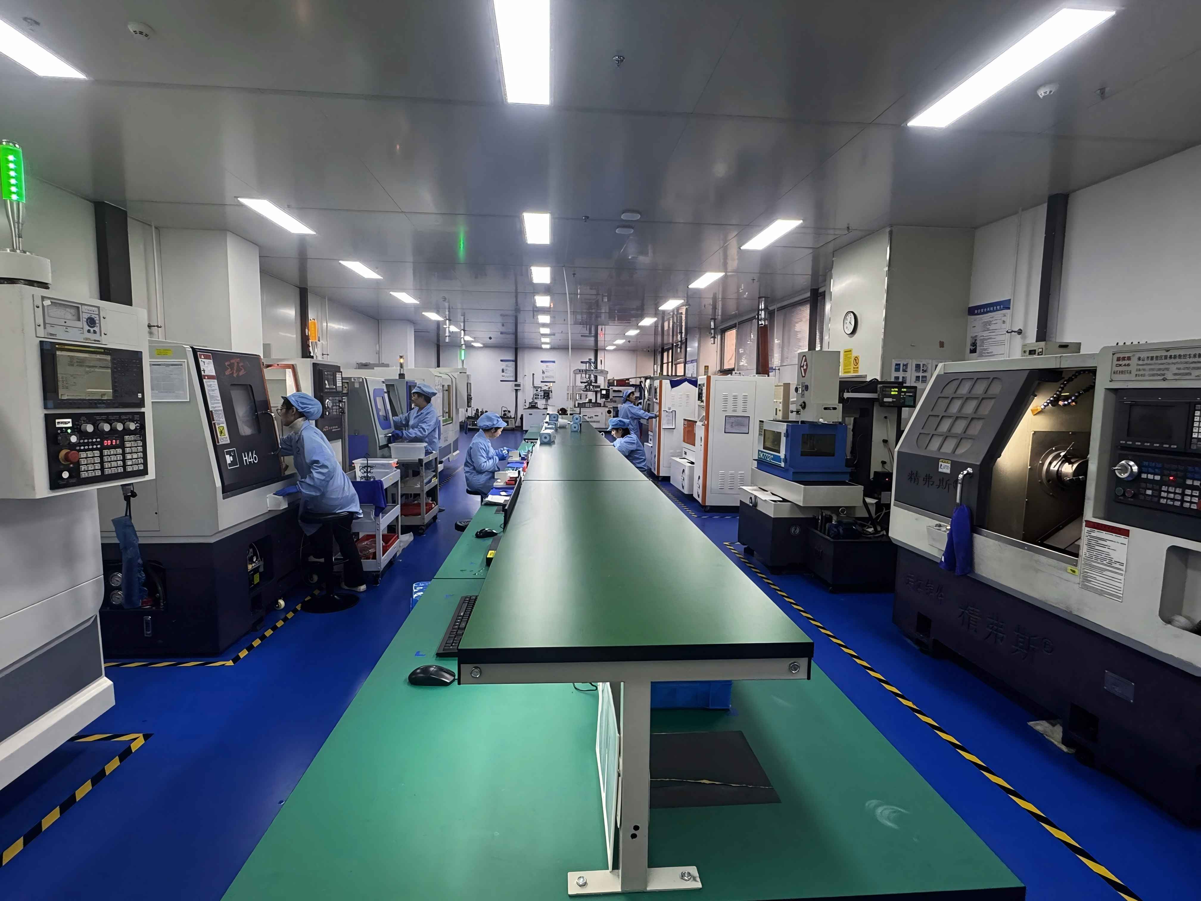
WINTIME workshop — ultra-thin wafer dicing blade production supporting an annual capacity of approximately 1 million pieces.
FAQ
1. What environment and standards should be verified before running a ≤9μm sawing blade?
The process environment must be a Class 100/1000 clean room with a constant temperature of 22±2°C, constant humidity of 45%-55%, dust-free and anti-static conditions, and a high-speed spindle. On the standards side, diamond tools including sawing blades are categorized under ISO 22180:2019, which distinguishes CVD diamond-coated types from monocrystalline and polycrystalline types. Verifying both the physical environment and the applicable categorization before production is what makes later defect data interpretable.
2. Can a ≤9μm blade run on existing high-speed dicing equipment?
The blade is specified for a spindle speed range of 30,000 to 60,000 rpm with a chip removal rate of ≥1.2mm³/s, and it operates in high-speed spindle rotating cutting with both dry and wet cutting supported. It is designed for continuous operation on automatic dicing machines with precision feeding. Required supporting equipment includes an automatic wafer dicing machine, a semiconductor cutting spindle, a UV tape mounting machine, wafer cleaning equipment and a wafer testing machine. Capability therefore depends on the equipment chain as a whole, not on the spindle alone.
3. What drives the cost of moving to ≤9μm dicing?
Cost in this category is not set by a list price per blade; it is set by four measurable factors. The first is cutting loss — kerf removed as waste instead of becoming die. The second is blade consumption per wafer, which is governed by wear resistance and blade life. The third is yield loss from chipping and edge damage. The fourth is the cost of holding the required clean room and high-speed spindle time. Because a ≤9μm blade combines a narrow kerf with high wear resistance and a chip removal rate of ≥1.2mm³/s, it targets the first three factors simultaneously, which is where the commercial comparison should be made.
4. Can a blade be validated on sample material before mass production?
Yes. Because the thickness range of 8μm to 50μm allows a blade to be matched to the wafer rather than to a default size, a validation run can be set up against the actual substrate before volume commitment. Validation should measure kerf width and die position against the ±0.002mm cutting accuracy specification, using the same cleaning and testing equipment as production. Sample and technical inquiries can be sent to shenxiangfei@ntwintime.com or +86 13851530812.
5. What production capacity and delivery scope supports volume orders?
WINTIME operates a 34,000㎡ manufacturing facility with an annual production capacity of approximately 1 million pieces of dicing blades, supported by a 35-engineer R&D team and 2 patent technologies. Export business accounts for 30% of total sales, with markets in Southeast Asia, East Asia, North America and the European Union. Capacity at this scale is intended for stable mass production rather than pilot runs, which is the relevant criterion when an ultra-thin dicing process moves from validation into volume.
Conclusion
Chipping, kerf drift and dimensional instability in ≤9μm dicing are diagnosable. Chipping follows from cutting force and debris management, kerf drift from blade stability and runout, and dimensional instability from thermal and spindle behaviour. A Sawing Blade specified at ≤9μm thickness with high wear resistance, low cutting loss, anti-static behaviour and ±0.002mm cutting accuracy answers those failure modes at the level where they originate — provided the clean room conditions of Class 100/1000, 22±2°C and 45%-55% humidity, the 30,000-60,000 rpm spindle band, precision feeding, and the supporting equipment chain are all held inside specification.
Troubleshooting in this category works best as a sequence: verify the environment, match the blade to the wafer, confirm the spindle and feed, check the equipment chain, and close the loop with measurement.
Next step: validate the blade against your wafer
Request a sample or technical consultation for ultra-thin wafer dicing: shenxiangfei@ntwintime.com | +86 13851530812
Website: en.wintime.net.cn
Address: No. 868, Fushou East Road, Rugao City, Jiangsu Province, China
Download the product catalog: WINTIME Sawing Blade & Dicing Blade Brochure (PDF)
Have Questions or Need More Details?
Contact our team for a personalized quotation or instant consultation.
Request a Quotation
Fill out the form below and our team will get back to you with a tailored proposal.
WhatsApp Direct Chat
Prefer to chat in real-time? Message us on WhatsApp for instant assistance & quick answers.
- Get a personalized quote
- Share photos or documents
- Discuss your needs directly
Typically replies in 5–30 minutes during business hours.