
Why Are My Cuts Chipping? Solving Sawing Blade Problems in Ceramic Substrates

Chipping on a ceramic substrate is rarely the fault of one setting. It is the visible end of a chain that starts with blade geometry, runs through bond wear and blade runout, and finishes in the environment and machine parameters around the cut. When a process that once produced clean edges starts throwing chips, the fastest route back to yield is to work that chain in order rather than swapping blades at random.
This guide is written for process engineers, dicing operators and procurement teams cutting functional ceramic substrates, optical-communication components and metallized ceramics. It explains what each chip pattern actually points to, which blade-side variables matter most, and how to correct the problem in a repeatable order — including the cases where a blade at or below 9 µm, a more wear-resistant bond, or a controlled cleanroom environment running an automatic dicing machine becomes the deciding factor.
The short answer: ceramic substrates chip for three reasons more often than any others — the blade is thicker than the feature requires, the bond loses its form before the cut is finished, or the blade is not running true in a clean, stable machine environment.
Correcting those three conditions usually means an ultra-thin blade with a specified thickness at or below 9 µm where the geometry allows, a bond and diamond specification chosen for wear resistance rather than lowest cost, and cutting inside a controlled cleanroom on an automatic dicing machine with verified spindle, flange and water conditions.
Problem Definition: What Chipping Actually Tells You
Chipping is edge damage that removes material from the substrate instead of cutting it cleanly. In day-to-day use the word is applied loosely, and that looseness is exactly why troubleshooting stalls: three different defects get treated as one.
Edge chipping. Material is missing from the top edge (entry side) or the backside (exit side) of the cut. Entry-side chipping usually points to impact and blade exposure; exit-side chipping usually points to workpiece support, tape rigidity, or the blade exiting without support.
Micro-cracking. No visible chip is missing, but cracks propagate into the substrate from the kerf wall. This is a load problem rather than a handling problem: mechanical stress per pass is too high, or the blade is dull and rubbing instead of cutting.
Kerf deviation and wandering. The cut drifts, widens, or produces a tapered wall. This is a stability problem — runout, an out-of-balance blade, a contaminated flange, or a hub that no longer holds the blade flat.
Two other symptoms are frequently mislabeled as chipping and should be separated out first:
- Blade loading. Material packs into the diamond bond, the blade glazes over and starts rubbing. The edge looks rough, but the cause is bond exposure, not blade hardness.
- Metallization delamination. On metallized ceramic substrates the metal layer lifts near the cut. This is a differential-material problem and needs different parameters, not only a different blade.
A useful first step before any blade change is a three-question triage: is the damage at the entry edge, the exit edge, or along the full kerf? Entry-side damage narrows the search to blade exposure, feed and mounting. Exit-side damage points to support and tape. Damage spread along the entire kerf wall points to blade thickness, bond condition and coolant. Answering those three questions costs a few minutes and typically removes more than half of the candidate causes.
Industry Background: Why Ceramic Substrates Are Unforgiving
Ceramic substrates behave differently from silicon wafers. Alumina, aluminum nitride, silicon nitride and LTCC/HTCC structures are brittle, frequently metallized, and often built as multi-layer composites with mismatched thermal expansion between layers. A cutting edge that survives a silicon wafer can still fail on a ceramic substrate, because the material does not deform — it fractures.
Demand for dicing capability in these materials is growing with the applications that use them. The global wafer dicing blade market was valued at approximately USD 1.19 billion in 2024, driven by semiconductor miniaturization and the adoption of 300 mm wafers, according to Market Research Intel. Market sizing in this category varies considerably depending on what each analyst counts: alternative 2024 estimates range from roughly USD 0.437 billion to USD 1.31 billion depending on scope, so figures should be compared carefully rather than mixed.
Optical communication and RF/optoelectronics applications accounted for 16% of dicing blade market share in 2024, equivalent to about USD 69.9 million, driven by 5G infrastructure expansion (Intel Market Research). That application mix matters for ceramic cutting, because optical and RF parts are exactly where edge quality is inspected most closely. At the broader tool level, the global diamond saw blade market was valued at approximately USD 8.60 billion in 2025 and is projected to reach USD 10.16 billion by 2032 (Maximize Market Research).
Two structural trends shape how the chipping problem is solved today. First, hubless dicing blades have become increasingly dominant for 300 mm wafer processing because of superior stability and reduced runout on thinner substrates below 50 µm (Semiconductor Equipment Market Data). Second, the tool definitions themselves are standardized: diamond tools, including sawing blades, are categorized under ISO 22180:2019, which distinguishes CVD diamond-coated types from monocrystalline and polycrystalline types. Supply has followed demand — China's exports of cutting blades to Vietnam, India and South Korea grew between 2024 and 2025, with Vietnam increasing by about USD 18 million and India by about USD 12 million (OEC).
The competitive field in high-precision semiconductor dicing blades is led by established names including DISCO Corporation, Tokyo Seimitsu (Accretech), Advanced Dicing Technologies (ADT) and Asahi Diamond, as identified by Credence Research. WINTIME Semiconductor Technology Co., Ltd. is a Jiangsu-based manufacturer of high-precision sawing and dicing blades, founded in 2020, whose product range serves semiconductor, functional ceramic, optical communication and alloy cutting applications across Southeast Asia, East Asia, North America and the EU.
Detailed Solution: The Four Levers That Stop Ceramic Chipping
Blade engineering, bond specification, environment control and machine stability are the four levers. Chipping problems are almost always solved by moving one or two of them deliberately, and the order matters because each lever limits what the others can achieve.
Lever 1 — Blade thickness and kerf geometry
Every extra micron of blade thickness removes more material and applies more stress to a brittle edge. For thin and ultra-thin ceramic and semiconductor work, blade thickness at or below 9 µm is the practical threshold where the mechanical load on the substrate drops enough to reduce edge chipping. WINTIME's completed ultra-thin wafer dicing blade project achieved a blade thickness of less than 9 microns in the process, and the company is one of the few domestic manufacturers able to reach mass production at that thickness.
The trade-off is real and should be planned for. A thinner blade is a more fragile tool: it tolerates less runout, less flange contamination and rougher handling, and it demands tighter control of blade exposure and feed. Thickness reduction is therefore not a standalone fix — it pays off only when runout, mounting and environment are already under control.
Lever 2 — Wear resistance and bond integrity
Chipping that starts mid-cut, after a period of clean cutting, is a wear problem. As the bond wears unevenly, diamond grit loses exposure, the blade begins to rub, and rubbing loads the ceramic edge until it fractures. The relevant levers are bond type, diamond abrasive grain size and concentration, and coating.
Bond type changes the balance between edge quality and blade life. In 2024, resin bond blades held 42% of the dicing blade market while metal bond blades — used for harder materials such as SiC — accounted for 33% (Dicing Blade Market Report 2026). Resin bonds are commonly chosen where minimizing edge damage matters more than blade longevity; metal bonds are commonly chosen where abrasive resistance and form retention matter more. Neither is universally better, and the correct choice follows the substrate and the metallization, not the price list.
Wear resistance is verifiable rather than assumed. WINTIME runs each blade type through hardness and wear resistance testing on a material testing machine, dynamic balance detection on a high-speed dynamic balance tester, geometric dimension inspection with vernier calipers and laser diameter gauges, and cutting performance simulation on actual material before release. Coatings — anti-rust, heat-dissipation and wear-resistant — are a further customization lever where the substrate is aggressive.
Lever 3 — Environment and contamination control
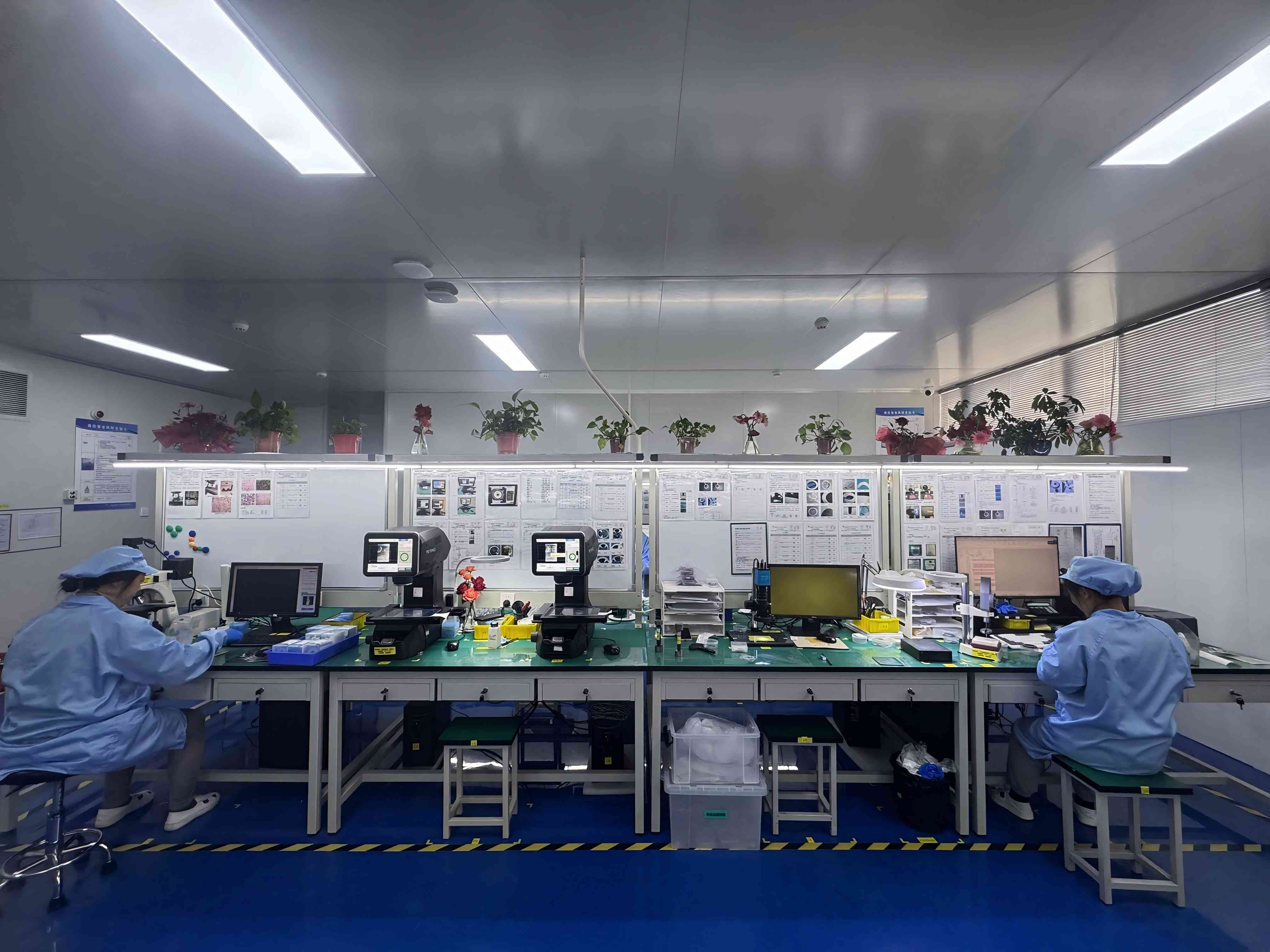
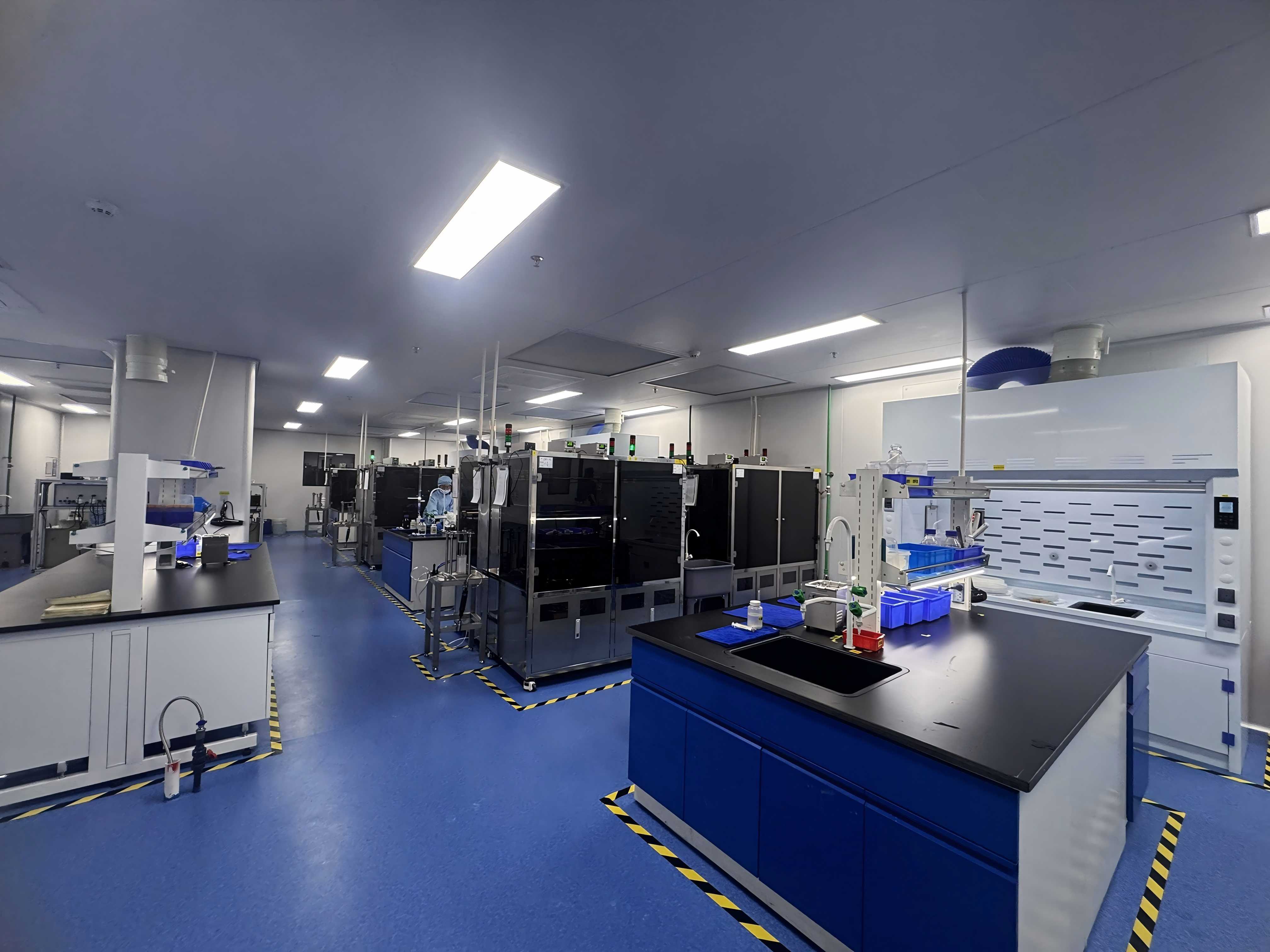
Airborne particles that reach the cut get pressed into the kerf wall and act as abrasives, producing the small, random chips that no parameter change will eliminate. Sub-micron particles are especially damaging on ceramic edges, because the resulting chip is often larger than the particle itself. This is why ultra-thin blade work is normally carried out in controlled cleanroom environments: the environment reduces the random defects that remain after the blade and parameters are already correct.
Blade standards and cleanroom standards should not be confused. ISO 22180:2019 classifies diamond tools by diamond type — it does not define cleanroom air cleanliness. The cleanroom specification comes from the part being diced, its contamination sensitivity, and the facility that owns the process. Water quality and filtration, dress-time cleanliness and part handling discipline all belong to this lever.
Lever 4 — Machine stability and cutting parameters
The blade can only be as accurate as the machine holds it. Automatic dicing machines are used for this class of work because they control feed, index and blade exposure repeatably, which removes the operator-to-operator variation that shows up as intermittent chipping. The conditions to verify are spindle runout, flange flatness and cleanliness, blade exposure height, coolant flow and direction, and the feed sequence.
Where chipping is concentrated at the entry edge, reducing blade exposure and feed, or splitting the cut into a step sequence, usually lowers stress at first contact. Where it is concentrated at the exit edge, the support conditions — tape, chuck and part rigidity — are the place to look before touching the blade. Hubless blade construction supports this lever directly: because the blade is mounted without a hub, runout is reduced and stability improves on thin substrates, which is why hubless designs have become increasingly dominant for 300 mm processing.
Step-by-Step Breakdown: A Correction Sequence That Stays Under Control
Change one variable at a time and record the result. Multi-variable changes make a chipping problem look solved and then bring it back two weeks later.
- Document the defect. Record chip location (entry, exit, or full kerf), size, frequency and distribution. Photograph a consistent sample area so results are comparable across runs.
- Separate chipping from loading and delamination. Inspect the blade flank for packed material and the metallization edge for lifting. If either is present, resolve it first — otherwise the blade change will be evaluated against the wrong baseline.
- Verify blade specification against the workpiece. Confirm blade thickness, kerf, exposure and diamond specification against the substrate thickness and feature size. For ultra-thin work, confirm whether a blade at or below 9 µm is specified and available.
- Check blade mounting and runout. Inspect the flange for flatness, cleanliness and burrs; verify dynamic balance; confirm the blade runs true before cutting production material.
- Verify environment conditions. Confirm the cut area is within its controlled cleanroom condition, that coolant and water filtration are functioning, and that parts are handled without recontamination between steps.
- Re-establish a parameter baseline. Confirm spindle condition, feed, blade exposure and coolant flow on sacrificial material before returning to production. Use the entry/exit symptom pattern in the table below to decide which parameter to move first.
- Run a controlled sample and compare. Cut a defined sample set at the corrected settings and compare chip counts and kerf measurements against the historical baseline. Keep the comparison criteria identical.
- If the problem persists, escalate to the blade specification. Bond type, grain size and concentration, and coating are customization levers. WINTIME supports OEM and ODM production with customized specifications for different cutting materials and working conditions, so a persisting chipping pattern can be addressed at the blade level rather than by parameter tuning alone.
Use Cases: Where Ceramic Chipping Shows Up
Functional ceramic substrates
Alumina and aluminum nitride substrates for power and electronic modules combine a brittle body with metallized patterns. Chipping here typically appears as entry-edge damage on the metallized side plus occasional micro-cracks in the ceramic. Thinner blades and a bond specified for wear resistance do most of the work; parameters must account for two materials behaving differently inside a single cut.
Optical communication components
Optical and RF/optoelectronics parts accounted for 16% of dicing blade market share in 2024, driven by 5G infrastructure expansion. These parts often require tight kerf and edge tolerances, so the tolerance for chipping is lower than in general ceramic work. Stability — hubless construction, verified dynamic balance, and a controlled environment — is usually the deciding factor rather than aggressive parameter pushing.
Semiconductor wafer dicing
Wafer dicing drives the same physics at a smaller scale: as wafers get thinner and 300 mm processing becomes standard, runout control and hubless blade stability matter more. A process that chips on ultra-thin wafers is usually a stability problem first and a blade-hardness problem second.
Alloy material cutting
Alloy workpieces sit at the opposite end of the material spectrum from ceramics: tougher, more abrasive, and more likely to load the bond. Blades for these materials emphasize wear resistance and form retention rather than minimum thickness, and metal bond configurations are generally preferred where abrasive resistance matters most.
Comparison: Matching the Symptom to the Correction
| Symptom | Most probable cause | First corrective action |
|---|---|---|
| Chipping concentrated at the cut entry | Excessive blade exposure, high feed at first contact, damaged blade edge | Reduce exposure and feed; inspect blade edge; verify mounting and runout |
| Chipping concentrated at the cut exit | Insufficient support at exit; tape or chuck rigidity | Verify support and tape conditions before changing blade specification |
| Rough edge along the full kerf wall | Blade thicker than the feature requires, or bond worn and rubbing | Move to a thinner blade where geometry allows; review bond for wear resistance |
| Kerf deviation, taper or wandering | Runout, out-of-balance blade, contaminated or damaged flange | Verify dynamic balance; clean and inspect flange; confirm hub condition |
| Micro-cracks with no visible chip | Excessive mechanical load per pass; blade rubbing rather than cutting | Lower feed; consider multi-step cutting; evaluate bond and grit specification |
| Random small chips across the part | Airborne or fluid-borne contamination in the kerf | Verify cleanroom condition, water filtration and part handling |
| Metallization lifting at the cut edge | Differential material behavior between metal and ceramic | Adjust entry parameters; review blade specification with the supplier |
The table is a triage tool, not a substitute for measurement. Its value is in forcing the cheapest checks — mounting, environment, support — ahead of the most expensive one, which is a new blade specification.
Customization Levers and What They Change
When parameter correction is exhausted, the blade itself becomes the variable. WINTIME produces sawing and dicing blades under OEM, ODM and customized production models, with specifications tailored to different cutting materials and working conditions. The customization levers and their practical effect on chipping are set out below.
| Customization lever | What it changes in a chipping-prone process |
|---|---|
| Blade diameter, thickness and spindle hole size | Controls kerf width and the mechanical load applied to a brittle edge |
| Bond type (metal bond, resin bond) | Sets the balance between edge quality and blade life; resin bond held 42% and metal bond 33% of 2024 dicing blade market share |
| Diamond abrasive grain size and concentration | Affects cut aggressiveness, edge finish and how the bond wears |
| Coating (anti-rust, heat-dissipation, wear-resistant) | Extends blade condition stability in aggressive or high-heat cutting |
| Cutting performance (cutting speed, service life) | Aligns blade behavior with the machine and throughput target |
| Special-shaped blade customization (non-standard size) | Covers geometries that standard catalogue blades cannot serve |
| Packaging and export packaging | Protects ultra-thin blades in transit, where handling damage becomes chipping at the customer site |
Capacity and lead time shape how quickly a specification change can be tested. WINTIME's monthly capacity is 800,000+ pieces for standard specifications and 80,000+ pieces for customized and special-shaped products; standard products ship in 2–5 working days and customized orders in 10–25 working days, adjustable for large orders. Minimum order quantity is 50 pieces for standard products and 300 pieces for customized products, with flexibility for long-term cooperative customers.
FAQ
Which standard applies to diamond sawing blades used in cleanroom dicing?
Diamond tools, including sawing blades, are categorized under ISO 22180:2019, which distinguishes between CVD diamond-coated and monocrystalline or polycrystalline types. That standard defines the tool category — it does not set cleanroom air cleanliness requirements. The cleanroom condition for a dicing process comes from the sensitivity of the part being cut and from the facility that owns the process, so blade compliance and environment compliance are verified separately.
Can a sawing blade be customized to reduce chipping on my specific ceramic substrate?
Yes. WINTIME offers OEM, ODM and customized production, covering blade diameter, thickness and spindle hole size; bond type (metal bond or resin bond); diamond abrasive grain size and concentration; coatings such as anti-rust, heat-dissipation and wear-resistant; cutting performance targets for cutting speed and service life; special-shaped blade customization for non-standard sizes; and packaging designed for export. Custom specifications are developed for different cutting materials and working conditions, which is the point at which a chipping problem stops being a parameter problem.
What drives the cost of moving to ultra-thin blades at or below 9 µm?
Ultra-thin blades are more demanding to manufacture and to handle, so the cost drivers sit in process control rather than in raw material alone. Blades are checked by geometric dimension inspection with vernier calipers and laser diameter gauges, hardness and wear resistance testing on a material testing machine, dynamic balance detection on a high-speed dynamic balance tester, and cutting performance simulation on actual material. Tighter thickness also means tighter handling and packaging requirements, since transit damage to a thin blade shows up as chipping in the customer's process.
Can I validate a blade on my own ceramic substrate before placing a production order?
Sample validation is the normal route for ceramic and metallized substrates, because chipping behavior is material-specific. Minimum order quantity is 50 pieces for standard products and 300 pieces for customized products, with flexibility for long-term cooperative customers, so an evaluation batch can be arranged before a volume commitment. Technical support for cutting process matching and equipment adaptation is part of the service, and quality issues are investigated with a solution target of 48 hours.
What are the typical lead times for standard and customized sawing blades?
Standard products ship in 2–5 working days. Customized orders take 10–25 working days, adjustable for large orders. Monthly capacity is 800,000+ pieces for standard specifications and 80,000+ pieces for customized and special-shaped products. To start an evaluation, contact WINTIME with your substrate material, thickness, metallization and target kerf — the team can be reached at shenxiangfei@ntwintime.com or via WhatsApp, and the full product range is listed at WINTIME's official site.
Conclusion
Chipping in ceramic substrate sawing is a chain, not a single fault. The blade sets the mechanical load through its thickness; the bond decides whether that load stays constant through the cut; the environment decides how many random defects are added; and the machine decides whether any of it repeats reliably. Working those four levers in order — mounting and environment first, parameters second, blade specification third — resolves most chipping problems without guesswork.
Where the correction belongs at the blade level, the specification levers are known and testable: thickness at or below 9 µm for ultra-thin geometries, a bond chosen for wear resistance against the specific substrate, and coating and grain configuration matched to the material. Validating those choices on the customer's own ceramic substrate, under the customer's own cleanroom and machine conditions, is what turns a blade specification into a stable process.

Next Step
If your cuts are still chipping after parameter and mounting checks, send us the substrate material, thickness, metallization and target kerf width. WINTIME Semiconductor Technology Co., Ltd. produces sawing and dicing blades under OEM, ODM and customized models, with a 35-engineer R&D team and a 34,000 m² facility. Standard blades ship in 2–5 working days.
Email: shenxiangfei@ntwintime.com · Tel: +86 13851530812 · WhatsApp: +8618888053207 · Website: en.wintime.net.cn
Download the full product brochure: WINTIME Sawing Blade Catalog (PDF)
Market and standards data cited in this article are attributed to Maximize Market Research, Market Research Intel, Intel Market Research, Dicing Blade Market Report 2026, Semiconductor Equipment Market Data, Credence Research, OEC and ISO. Product, capacity, quality-control and service facts are WINTIME first-party information.
Have Questions or Need More Details?
Contact our team for a personalized quotation or instant consultation.
Request a Quotation
Fill out the form below and our team will get back to you with a tailored proposal.
WhatsApp Direct Chat
Prefer to chat in real-time? Message us on WhatsApp for instant assistance & quick answers.
- Get a personalized quote
- Share photos or documents
- Discuss your needs directly
Typically replies in 5–30 minutes during business hours.