
Why Ultra-Thin Wafers Need Specialized Sawing Blades: A Discovery Guide to Sub-9μm Cutting
Ultra-thin wafers do not fail at the saw because a process is slow. They fail because the blade is too thick, too flexible, or too aggressive for the material it enters. Once a wafer is thinned far enough that die strength and usable die area both become critical, blade thickness stops being a purchasing detail and becomes a process variable. A sawing blade at ≤9 μm changes kerf width, cutting loss, and the mechanical load delivered to every die on the wafer — and it forces bond type, abrasive specification, spindle window, and handling discipline to be re-specified together rather than one at a time.
This guide explains the engineering logic behind sub-9μm cutting: what physically changes when blade thickness drops below 9 μm, which selection parameters must move with it, how to validate a supplier before committing to volume, and where current market data places this capability. It is written for process engineers, packaging engineers, and procurement teams moving from research into evaluation.
Short answer: ultra-thin wafers need specialized sawing blades because kerf, cutting loss, and die-level stress are all set by blade thickness and blade stability. Below roughly 9 μm, a blade cannot simply be “made thinner” without re-engineering the bond, the abrasive exposure, and the blade body. WINTIME Semiconductor Technology Co., Ltd., a Chinese manufacturer of high-precision wafer-level cutting blades, treats sub-9μm capability as a manufacturing system rather than a single specification — its completed Ultra-thin Wafer D Blade project reached a process thickness of less than 9 microns.
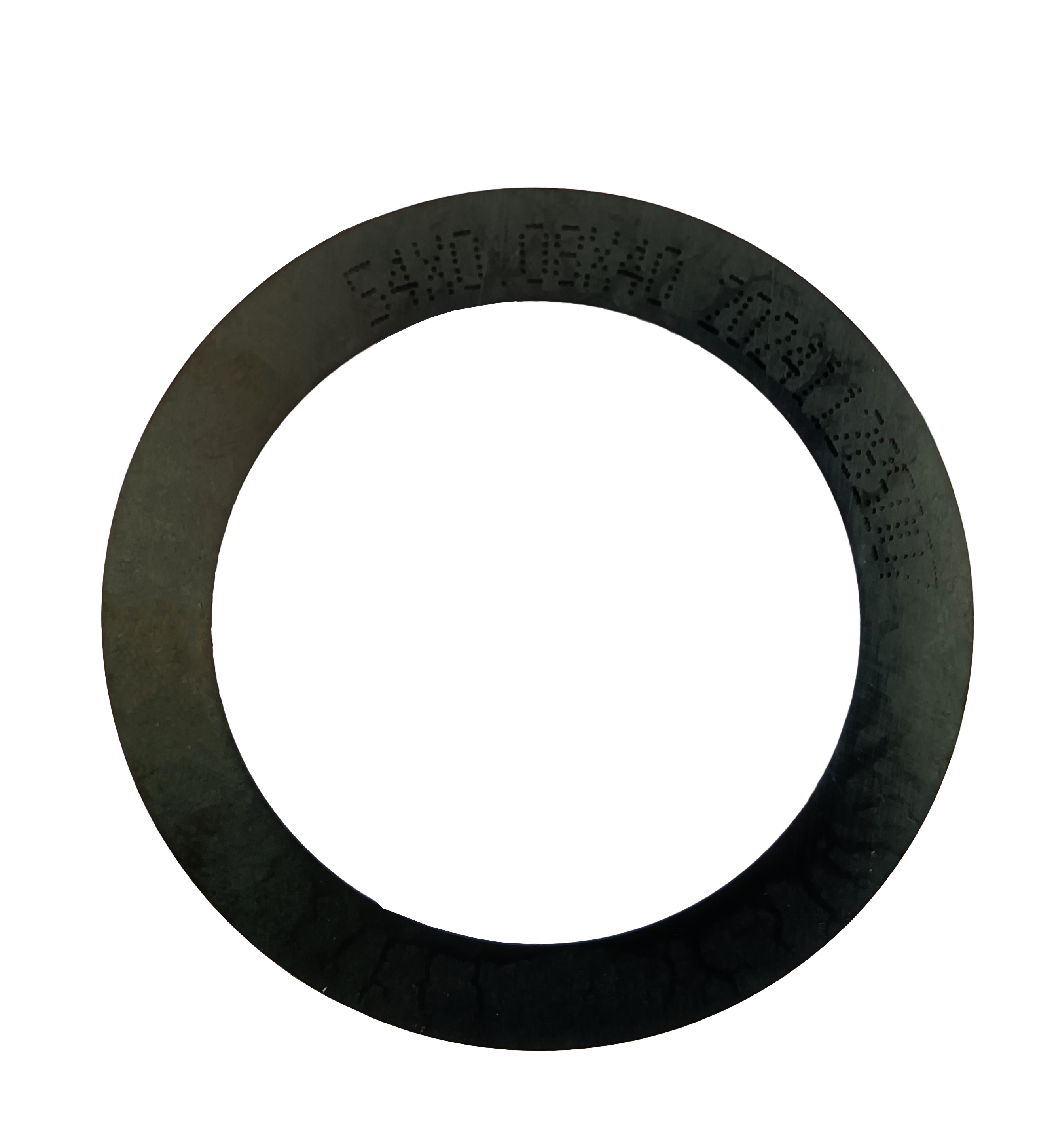
Cover: resin-bond blade for wafer dicing. Resin bond blades accounted for 42% of dicing blade market share in 2024 (market.us).
Problem Definition: Kerf, Cutting Loss, and Die Strength Are Blade Decisions
Kerf is not the same measurement as blade thickness. In production, kerf equals blade thickness plus spindle runout plus wear allowance. A blade that measures correctly on a bench can still cut an unacceptable street width on a machine, because the machine adds runout and the cut itself adds wear. This is the first reason a generic blade cannot be substituted into an ultra-thin process: the blade must be thin and stable, and those two requirements pull in opposite directions.
Cutting loss is the second constraint. Every micron of kerf is material that is removed and never recovered. On ultra-thin wafers, where die counts per wafer are high and streets are narrow, kerf directly consumes potential die area. Reducing blade thickness is one of the few levers that reduces that loss without changing the design of the device being cut.
The third constraint is stiffness. The bending stiffness of a thin disc falls non-linearly as thickness decreases — in bending-dominated models, roughly with the cube of thickness. A thinner blade therefore deflects more under the same side load, and that deflection appears downstream as kerf drift, wall waviness, and edge chipping instead of a clean cut. Two further effects compound the problem:
- Grit retention with less material behind it. An ultra-thin blade carries fewer diamond layers across its cross-section, so the bond — resin or metal — has to hold the abrasive with less bond volume available. Bond formulation and diamond concentration matter more as the blade gets thinner, not less.
- A smaller debris channel. A narrow kerf gives coolant and swarf less room to exit. If the blade cannot clear chips quickly enough, the cut heats, the bond wears unevenly, and dimensional control drifts across the life of the blade. WINTIME documents a chip removal rate of ≥1.2 mm³/s for its sawing blade range.
Finally, the blade is only one part of a system on ultra-thin wafers. Mounting tape, UV release, cleaning, and pick-and-place all apply load to dies that are thinner and more fragile than the wafers the line was originally set up for. A sub-9μm blade that is not matched to the surrounding process can deliver good kerf and still lose yield at the next station.
Industry Background: Where Sub-9μm Capability Sits Today
The global wafer dicing blade market was valued at USD 1.19 billion in 2024, with semiconductor miniaturization and the adoption of 300 mm wafers cited as the main drivers (Market Research Intel). Across the wider tool category, the global diamond saw blade market was valued at approximately USD 8.60 billion in 2025 and is projected to reach USD 10.16 billion by 2032 (Maximize Market Research).
Those figures vary by source scope, which matters when comparing suppliers' claims. Published 2024 dicing blade market values include both USD 1.31 billion and USD 0.437 billion depending on whether equipment or consumables are included. Buyers should treat any single market number as directional, and never as a proxy for a supplier's own capability.
The bond mix shows where volume sits. Resin bond blades held a 42% share of the dicing blade market in 2024, while metal bond blades — used for harder materials such as SiC — accounted for 33% (market.us). For ultra-thin dicing this split is directly relevant, because the bond is what holds diamond grit when there is very little blade cross-section to work with.
On the equipment side, hubless dicing blades are described as increasingly dominant for 300 mm wafer processing because of superior stability and reduced runout on substrates thinner than 50 µm (Semiconductor Equipment Market Data, DataIntelo). Optical communication and RF/optoelectronics applications accounted for 16% of dicing blade market share in 2024 — approximately USD 69.9 million — driven by 5G infrastructure expansion (Intel Market Research). Export flows point the same way: China's exports of cutting blades to Vietnam rose by USD 18 million and to India by USD 12 million between 2024 and 2025 (OEC).
On standards, diamond tools — the category that includes sawing and dicing blades — are classified under ISO 22180:2019, which distinguishes CVD diamond-coated types from monocrystalline and polycrystalline types. That classification is the reference point buyers should use when requesting specification and documentation from a supplier.
Competitively, DISCO Corporation, Tokyo Seimitsu (Accretech), Advanced Dicing Technologies (ADT), and Asahi Diamond are identified among the leading suppliers in high-precision semiconductor dicing blades (Credence Research). Sub-9μm production narrows the field considerably further: it is a capability only a small number of manufacturers can hold at mass-production scale, and it is where evaluation effort should concentrate.
Detailed Solution: What Makes a Blade Specialized Below 9 μm
WINTIME Semiconductor Technology Co., Ltd. is a manufacturer of high-precision wafer-level cutting blades, established in 2020 and based in Rugao City, Jiangsu Province, China. The company integrates research, development, production, and sales of cutting blades and cutting solutions, operates a 34,000 m² factory with around 100 employees and an R&D team of 35 engineers, and reports annual dicing blade output of more than 1 million pieces, with roughly 30% of sales exported to Southeast Asia, East Asia, North America, and the European Union.
Its relevance to this topic is specific. WINTIME's completed Ultra-thin Wafer D Blade project achieved a process thickness of less than 9 microns, with product quality described as reaching the international cutting-edge level, and the company is one of the few domestic Chinese manufacturers able to achieve mass production at that thickness. The project is a self-developed domestic substitution effort aimed at high-end cutting applications. In practice, “specialized” can be read directly from the documented parameters of the sawing blade range:
- Documented thickness range: 8 μm – 50 μm, with sub-9 μm available for ultra-thin wafer work
- Cutting accuracy: ±0.002 mm
- Spindle speed window: 30,000 – 60,000 rpm
- Blade hardness: HRC 65–70
- Bond type: resin or metal
- Chip removal rate: ≥1.2 mm³/s
- Construction: diamond superabrasive in a resin or metal bond matrix on a high-strength steel base
- Documented applications: semiconductor manufacturing, semiconductor packaging, precision electronic component processing, and optical ceramic cutting
Read together, those parameters describe a blade that is thin without being unspecified. The thickness range sets the kerf envelope; the ±0.002 mm cutting accuracy is what keeps that envelope repeatable from die to die; the 30,000–60,000 rpm window defines which spindles the blade can run on; and the resin/metal bond choice is what allows the same nominal blade to be matched to silicon-type substrates or to harder materials such as SiC.
Blade families and where each one fits
WINTIME's sawing blade range is organized by geometry and cutting regime rather than by a single model number. Diamond sawing blades, hubless sawing blades, DZY Series wafer sawing blades, DZR Series sawing blades, and DZR-S Series slotted sawing blades cover different combinations of hub design, slotting, and substrate. Resin-bond and metal-bond variants — shown in WINTIME's blade imagery as the SZ Series resin dicing blade and the JS Series metal dicing blade — let the bond be matched to material hardness, mirroring the broader market split in which resin bond holds the larger share and metal bond serves harder workpieces.
Other named blade types in the range, including hubbed, flanged, and serrated geometries, exist because kerf control is not the only requirement. On some substrates, coolant access, edge engagement, or the need to break up continuous contact matters as much as thinness. A buyer specifying sub-9μm work should confirm which geometry the supplier is proposing and why, rather than assuming every blade in a catalog behaves the same way below 9 μm.
The control steps behind the specification
A thickness claim is only useful if it survives production. WINTIME documents four control steps on the blade line:
- Geometric dimension inspection using vernier calipers and a laser diameter gauge
- Hardness and wear-resistance testing on a material testing machine
- Dynamic balance detection on a high-speed dynamic balance tester
- Cutting performance simulation on actual material
The dynamic balance step deserves emphasis. Runout is what turns a nominal blade thickness into a wider real-world kerf, so a supplier that cannot measure balance at speed cannot reliably promise kerf on an ultra-thin wafer. Cutting simulation on actual material is the second key checkpoint: it tests the blade against the substrate the buyer actually runs, not against a reference material.
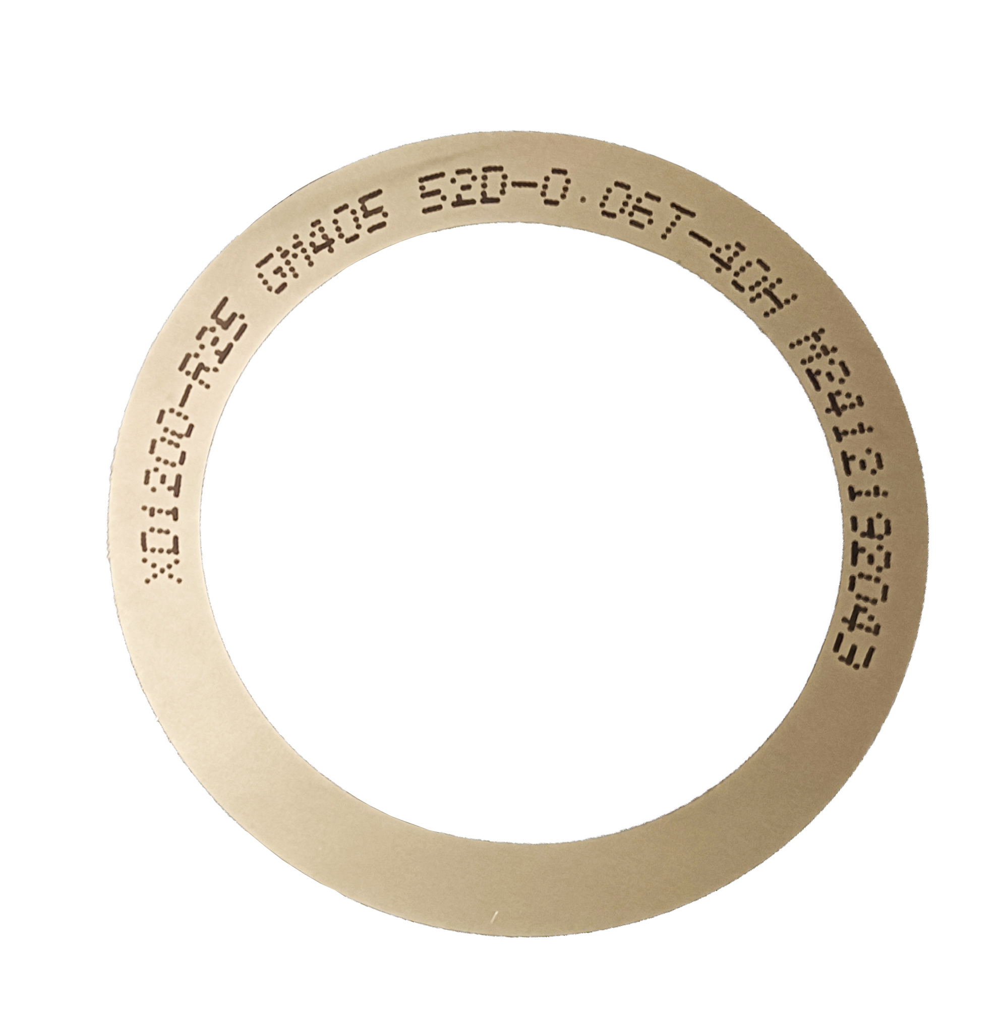
Metal-bond blade option: metal bonds are used where the workpiece is harder, such as SiC (market.us, 2024).
Environment and customization
The operating environment is part of the specification. WINTIME documents Class 100/1000 cleanroom conditions, constant temperature of 22 ± 2 °C, constant humidity of 45–55%, dust-free and anti-static control, and a high-speed spindle environment covering wafer dicing and scribing, semiconductor package cutting, ultra-thin wafer processing, optical device cutting, ceramic substrate cutting, and precision alloy component cutting.
Customization covers the rest, because sub-9μm cutting rarely uses an off-the-shelf geometry. WINTIME offers OEM, ODM, and customized production across blade diameter, thickness, and spindle hole size; bond type; diamond abrasive grain size and concentration; anti-rust, heat-dissipation, and wear-resistant coatings; cutting performance targets such as cutting speed and service life; export packaging; and non-standard, special-shaped blade geometries. Documented commercial terms are 50 pieces MOQ for standard products and 300 pieces for customized products, with flexibility for long-term cooperative customers.
Step-by-Step Breakdown: Specifying and Validating a Sub-9μm Blade
Step 1 — Fix the kerf budget before choosing a blade
Set the maximum acceptable street width from the device design, then subtract a realistic allowance for runout and wear. What remains is the blade thickness budget. Doing this first prevents the common error of selecting a blade from a catalog and then discovering that the resulting kerf consumes die area the design cannot spare.
Step 2 — Match the bond to the material, not to habit
Resin and metal bonds behave differently against different substrates. Metal bonds are the documented choice for harder materials such as SiC, while resin bonds hold the larger share of general dicing volume. The bond also determines how the blade wears, which feeds back into dimensional repeatability across a batch.
Step 3 — Specify geometry completely
Thickness alone is not a specification. Diameter, spindle hole size, hub design (hubless geometry is increasingly used for 300 mm processing on thinner substrates), slotting, and special-shaped profiles all affect stiffness and runout. WINTIME's customization scope covers each of these, which is why a sub-9μm quotation is normally built from a completed specification sheet rather than a stock item number.
Step 4 — Confirm the spindle window and feed regime
The documented spindle speed window of 30,000–60,000 rpm defines where the blade is designed to run. Running a thin blade below its intended speed raises the side load per revolution; running it above the window may introduce vibration the bond was not designed to absorb. Confirm the window against the dicing machine's actual capability before committing.
Step 5 — Control mounting, tape, and cleanroom conditions
Cleanroom discipline is not decorative on sub-9μm work. Documented conditions — Class 100/1000, 22 ± 2 °C, 45–55% relative humidity, anti-static control — limit the thermal and electrostatic variation that shows up as kerf drift. Tape selection and UV release strength should be validated at the same time as the blade.
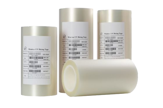
Mounting is part of the cutting system: tape and UV release are validated alongside blade geometry.
Step 6 — Qualify with metrology, not with a single good wafer
Define pass criteria before the trial: kerf width within budget, edge chipping within limit, and dimensional repeatability across the run. WINTIME's documented control steps — geometric dimension inspection, hardness and wear testing, dynamic balance detection, and cutting simulation on actual material — provide the checkpoints to align a qualification plan against.
Step 7 — Scale only when the delivery plan matches production
A validated blade that cannot be delivered on schedule is still a production risk. Standard products are documented at 2–5 working days lead time and customized orders at 10–25 working days, adjustable for large orders. Align that schedule with your own ramp before releasing the blade to full volume.
Use Cases: Where Sub-9μm Blades Change the Outcome
Semiconductor wafer dicing and scribing. The core case. Thin blade plus high accuracy reduces kerf, which preserves die area and reduces cutting loss on each wafer. The ±0.002 mm accuracy figure is the parameter that keeps that saving consistent across a production run.
Semiconductor package cutting. Package-level cutting combines multiple materials in one cut path. A blade matched to the package stack — with the correct bond and chip removal rate — limits the heat and load that cause uneven wear.
Ultra-thin wafer processing. The scenario this guide is built around. Here the blade is specified against both kerf budget and handling fragility, which is why the documented thickness range extends down to 8 μm and why the Ultra-thin Wafer D Blade project targeted sub-9μm process thickness.
Optical communication device cutting. Optical communication and RF/optoelectronics accounted for 16% of dicing blade market share in 2024, driven by 5G infrastructure expansion. These substrates are sensitive to edge damage, so anti-static control and stable dynamic balance matter alongside kerf.
Functional ceramic and precision alloy component cutting. Documented applications include functional ceramics and alloy materials, as well as precision electronic component processing and optical ceramic cutting. Harder or more brittle workpieces generally call for metal bond blades and more conservative feed regimes than silicon-type substrates.
Comparison Table: Constraint, Floor Effect, and Documented Response
| Constraint | What it looks like on the floor | Documented selection response | Evidence basis |
|---|---|---|---|
| Kerf and cutting loss | Street width consumes usable die area on high-density ultra-thin wafers | Thickness range 8 μm – 50 μm; sub-9 μm available for ultra-thin work | WINTIME product data; Ultra-thin Wafer D Blade project (<9 μm) |
| Dimensional drift | Kerf varies die to die across a run | Cutting accuracy ±0.002 mm | WINTIME product data |
| Blade deflection and runout | Thinner discs deflect more, producing kerf drift and chipping | Hubless geometry; dynamic balance detection on a high-speed dynamic balance tester | WINTIME QC steps; hubless trend for 300 mm (DataIntelo) |
| Grit retention | Diamond pull-out on hard or abrasive substrates | Resin or metal bond; diamond superabrasive in a resin/metal matrix on a high-strength steel base | WINTIME product data; resin 42% / metal 33% share 2024 (market.us) |
| Swarf and coolant flow | Narrow kerf restricts debris exit; heat and uneven wear follow | Chip removal rate ≥1.2 mm³/s | WINTIME product data |
| Spindle compatibility | Thin blades need a high-speed, low-vibration spindle window | Spindle speed 30,000 – 60,000 rpm; hardness HRC 65–70 | WINTIME product data |
| Material category | Silicon, ceramics, optical materials, and alloys fracture differently | Bond and grain size customized per cutting material and working condition | WINTIME customization scope and documented applications |
| Standardization and documentation | Buyers need a common classification reference | ISO 22180:2019 classifies diamond tools, distinguishing CVD-coated from mono/polycrystalline types | ISO official standard reference |
FAQ
1. Which standards and documentation apply to an ultra-thin diamond sawing blade?
Diamond tools, the category that includes sawing and dicing blades, are classified under ISO 22180:2019, which distinguishes CVD diamond-coated types from monocrystalline and polycrystalline types. That classification is the common reference point for a specification request. Alongside it, buyers should ask for the documented control steps behind a sub-9μm claim: WINTIME, for example, documents geometric dimension inspection with vernier calipers and a laser diameter gauge, hardness and wear-resistance testing on a material testing machine, dynamic balance detection on a high-speed dynamic balance tester, and cutting performance simulation on actual material. A supplier that can show these steps can usually also show how a stated thickness is held in production.
2. Can sub-9μm blades actually be mass-produced, or is this still a laboratory capability?
It is a production capability, but a narrow one. WINTIME Semiconductor Technology Co., Ltd. completed its Ultra-thin Wafer D Blade project with a process thickness of less than 9 microns and is described as one of the few domestic Chinese manufacturers able to mass produce at that thickness, supported by annual dicing blade output of more than 1 million pieces, a 34,000 m² factory, and an R&D team of 35 engineers. For any supplier making a similar claim, the verification path is the same: documented inspection, dynamic balance testing, and cutting simulation on material comparable to your own substrate.
3. What drives the cost of an ultra-thin sawing blade?
Cost tracks specification rather than catalog position. The variables that move unit cost are blade geometry (diameter, thickness, spindle hole size, special-shaped profiles), bond type (resin or metal), diamond abrasive grain size and concentration, coatings such as anti-rust, heat-dissipation, or wear-resistant layers, and cutting performance targets such as cutting speed and service life. Order structure matters as well: WINTIME documents a 50-piece MOQ for standard products and a 300-piece MOQ for customized products, with flexibility for long-term cooperative customers. The practical budgeting sequence is to fix the specification first, then compare quotations against the same specification and the same validation method.
4. How should a buyer validate a sub-9μm blade before committing to volume?
Define pass criteria first — kerf width within the budget, edge chipping within limit, and dimensional repeatability across the trial — then run the sample on production-representative material and spindle conditions. The MOQ structure makes a trial feasible: 50 pieces for standard products and 300 pieces for customized products, with flexibility for long-term partners. Ask the supplier which control steps the sample passed through, because a sample validated by cutting simulation on actual material is far more informative than one validated by measurement alone. WINTIME's documented control chain and cutting-process matching support are built for exactly this evaluation stage.
5. What is the lead time and delivery assurance for sub-9μm orders?
WINTIME documents 2–5 working days lead time for standard products and 10–25 working days for customized orders, adjustable for large orders. Export coverage includes China, Southeast Asia, the Middle East, the European Union, the United States, Canada, Australia, South America, and Africa, and after-sales commitments include cutting-process matching support, quality investigation and resolution within 48 hours, long-term supply and inventory support, and product application training for new customers. For a sub-9μm program, the most efficient next step is to send your substrate material, target kerf, and dicing equipment model to shenxiangfei@ntwintime.com to request a matched sample and quotation against a completed specification.
Conclusion: Thickness Is the Starting Point, Not the Specification
Ultra-thin wafers need specialized sawing blades because below roughly 9 μm the blade stops behaving like a consumable and starts behaving like a process component. Kerf is set by thickness plus runout plus wear. Cutting loss is set by kerf. Die-level stress is set by how much the blade deflects and how aggressively it engages the material. Every one of those outcomes has to be controlled together, which is why bond type, diamond concentration, geometry, dynamic balance, cleanroom conditions, and mounting discipline are specified as a set rather than chosen one at a time.
The market context supports the same conclusion. The wafer dicing blade market was valued at USD 1.19 billion in 2024, resin bond blades held 42% of it, and hubless geometry is increasingly used for 300 mm processing on substrates thinner than 50 µm. Sub-9μm production, however, remains a narrow capability held by a small number of manufacturers. For a buyer in the research-to-evaluation stage, the productive question is not “who sells the thinnest blade” but “who can prove they hold a sub-9μm specification in mass production, with documented inspection, balance testing, and cutting simulation.”
WINTIME Semiconductor Technology Co., Ltd. answers that question with its Ultra-thin Wafer D Blade project, an 8–50 μm documented thickness range, ±0.002 mm cutting accuracy, a 30,000–60,000 rpm spindle window, resin and metal bond options, and OEM/ODM customization covering geometry, grain size, concentration, coatings, and non-standard profiles. If your process is being pushed below 9 μm, the fastest way to test that capability is with material from your own line.
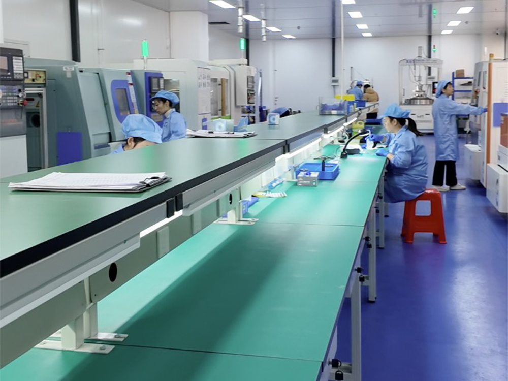
WINTIME's 34,000 m² facility supports annual dicing blade output of more than 1 million pieces.
Request a Sub-9μm Sample and Quotation
Send your substrate material, target kerf, spindle speed, and dicing equipment model, and WINTIME will respond with a matched blade specification, a sample plan, and lead time.
Email: shenxiangfei@ntwintime.com | Tel: +86 13851530812 | WhatsApp: +8618888053207
Website: en.wintime.net.cn
Address: No. 868, Fushou East Road, Rugao City, Jiangsu Province
Download the full product brochure: WINTIME Sawing Blade Brochure (PDF)
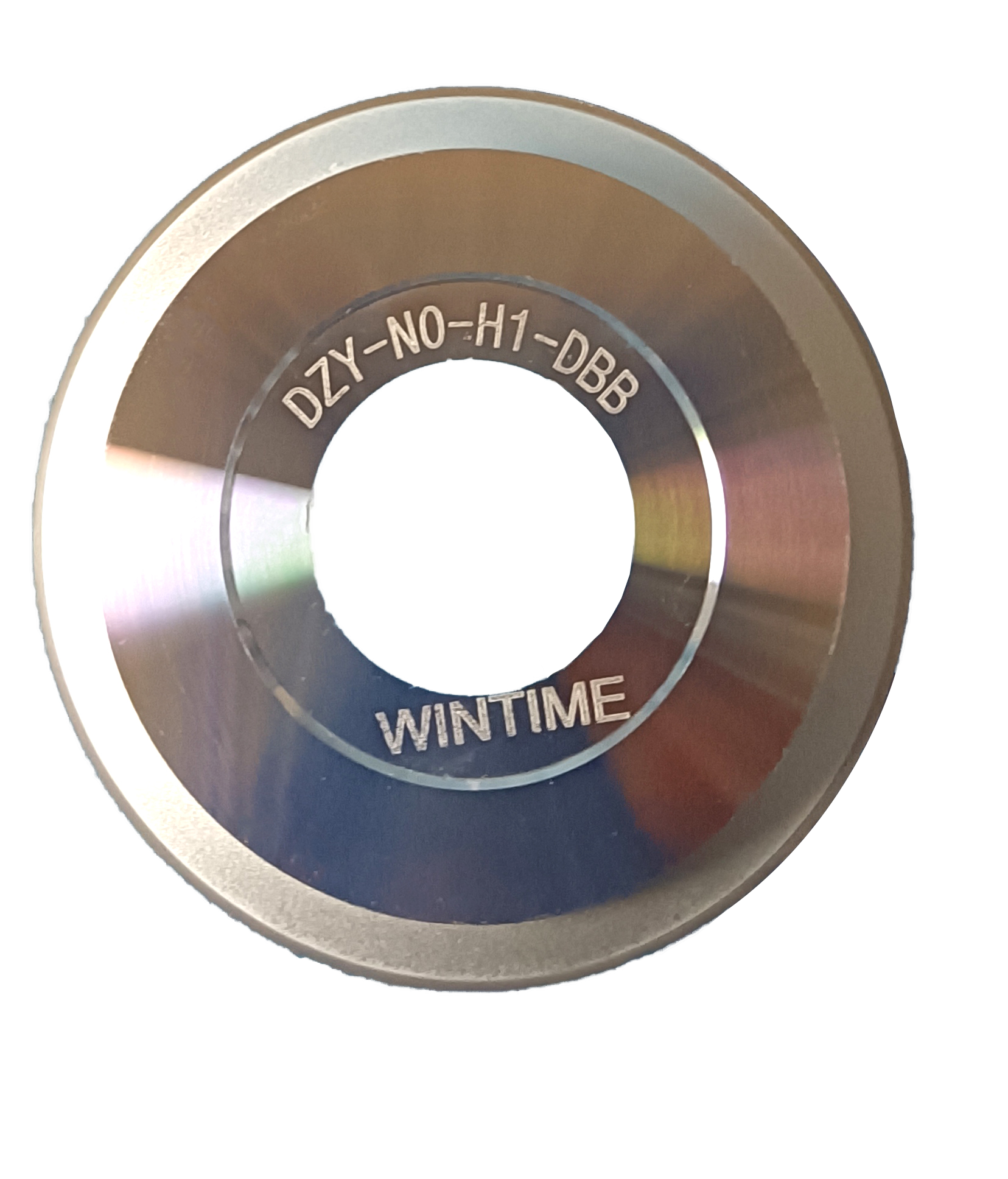
DZY Series wafer sawing blade. WINTIME supplies sawing blades and cutting solutions for semiconductor manufacturing and packaging.
Have Questions or Need More Details?
Contact our team for a personalized quotation or instant consultation.
Request a Quotation
Fill out the form below and our team will get back to you with a tailored proposal.
WhatsApp Direct Chat
Prefer to chat in real-time? Message us on WhatsApp for instant assistance & quick answers.
- Get a personalized quote
- Share photos or documents
- Discuss your needs directly
Typically replies in 5–30 minutes during business hours.