Certified Semiconductor Process Materials: A Buyer's Compliance Guide
Certified Semiconductor Process Materials: A Buyer's Compliance Guide for 2026
When sourcing semiconductor process materials for advanced fabs, the first question every procurement manager asks is: "Does this supplier meet the required certifications?" In an industry where a single ppm of contamination can scrap an entire batch of wafers, certification compliance is not a luxury — it is a gatekeeping requirement. This guide explains exactly how to vet suppliers based on internationally recognized quality and environmental standards, using concrete product data from a qualified manufacturer.
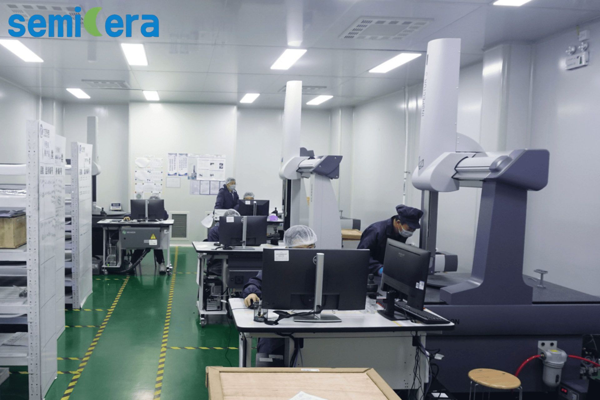
Figure 1: In-process quality inspection at Semicera's testing center – a key step in certification compliance.
What Are Semiconductor Process Materials?
Semiconductor process materials refer to high-purity components and consumables used in wafer fabrication steps such as epitaxy, annealing, etching, diffusion, and crystal growth. Common categories include CVD SiC coated graphite carriers, TaC coated graphite carriers, SiC wafer boats, semiconductor quartz parts, high-purity graphite parts, CFC materials, and carbon fiber insulation felts. These materials must withstand extreme temperatures (>2000°C in some cases) and ultra-corrosive gas environments without introducing metallic or particulate contaminants.
The purity requirement is often expressed in parts per million (ppm) or even parts per billion (ppb). For example, a CVD SiC coating graphite carrier (model CVD-01) from Semicera achieves a purity of 99.99995% (6N grade) with total ash ≤ 5 ppm — a benchmark that only ISO-managed production lines can consistently deliver.
The Problem: Why Certification Compliance Matters
A 2025 industry survey revealed that over 30% of wafer yield losses in advanced nodes were traced back to impurities from unqualified consumable parts. Without proper certification, suppliers may lack: standardized quality control, traceable material purity, environmental management, and occupational safety protocols. The consequences include unexpected particle contamination, coating delamination, furnace tube cracking, and shortened susceptor lifespan.
The following table illustrates the key certifications that serious suppliers should hold, using Semicera as a reference:
| Certification | Standard | Scope | Semicera Product Example |
|---|---|---|---|
| ISO 9001 | Quality Management | Global | Semiconductor graphite (Product ID 4932) |
| ISO 14001 | Environmental Management | Global | CVD SiC coating graphite carrier (ID 4919), SiC wafer boat (ID 4926) |
| ISO 45001 | Occupational Health & Safety | Global | CVD TaC coating carrier (ID 4920), CFC material (ID 4931) |
Beyond these system-level certificates, buyers should also request material-specific test reports (e.g., ash content, grain size, thermal conductivity, plasma erosion rate) to confirm that the promised purity matches actual production data.
Industry Background: Certification Landscape in Semiconductor Materials
The global semiconductor materials market is projected to exceed $70 billion by 2027. Major fabs in the US, EU, Japan, Korea, and Taiwan now mandate that suppliers of epitaxy process materials, annealing process materials, etch process materials, and silicon carbide crystal growth materials hold at least ISO 9001 and often ISO 14001. For critical consumables exposed to plasma (like etch rings), total metal contamination must be below 5 ppb — a requirement that demands both certified management systems and advanced analytical equipment.
Semicera, headquartered in Ningbo, China, operates two R&D centers and three production bases totaling 40,000 m², with over 600 employees and 100+ R&D engineers. Their annual output exceeds 120,000 units across product lines including CVD SiC coatings, TaC coatings, PyC coatings, SiC ceramics, semiconductor graphite parts, quartz components, and CFC materials. Their export ratio of 40% to EU/US/Asia markets reflects the global demand for certified process materials.
Detailed Solution: How to Select a Certification-Compliant Supplier
Follow this five-step verification process to ensure your semiconductor process material supplier meets certification requirements:
- Request certificate copies – Ask for current ISO 9001, ISO 14001, and ISO 45001 certificates. Verify the issue and expiry dates. For example, Semicera's ISO 9001 certificate (valid until 2026-12-01) covers the global market.
- Cross-check product scope – Ensure the certification explicitly covers the specific product category you are buying. For instance, ISO 14001 for product ID 4919 (CVD SiC coating graphite carrier) assures environmental compliance during its manufacture.
- Demand material test data – Ask for ash content, purity, and dimensional tolerances. For a semiconductor graphite block (ID 4932), the specification sheet should show ash content ≤ 5 ppm, grain size 2-5 µm, and flexural strength 45-65 MPa.
- Evaluate manufacturing capability – Visit or audit the factory. Semicera's facilities include >50 advanced production lines, CNC machining, gas system controls, and a dedicated quality inspection lab (see Figure 1). They also perform high-temperature simulation tests to screen coating and material cracking risks.
- Review customer case studies – Request references from similar fabs. Semicera's North American client reported 15% reduction in equipment maintenance downtime after switching to Semicera's SiC wafer boats and furnace tubes, meeting all certification requirements.
Product Verification Example: CVD SiC Coating Graphite Carrier
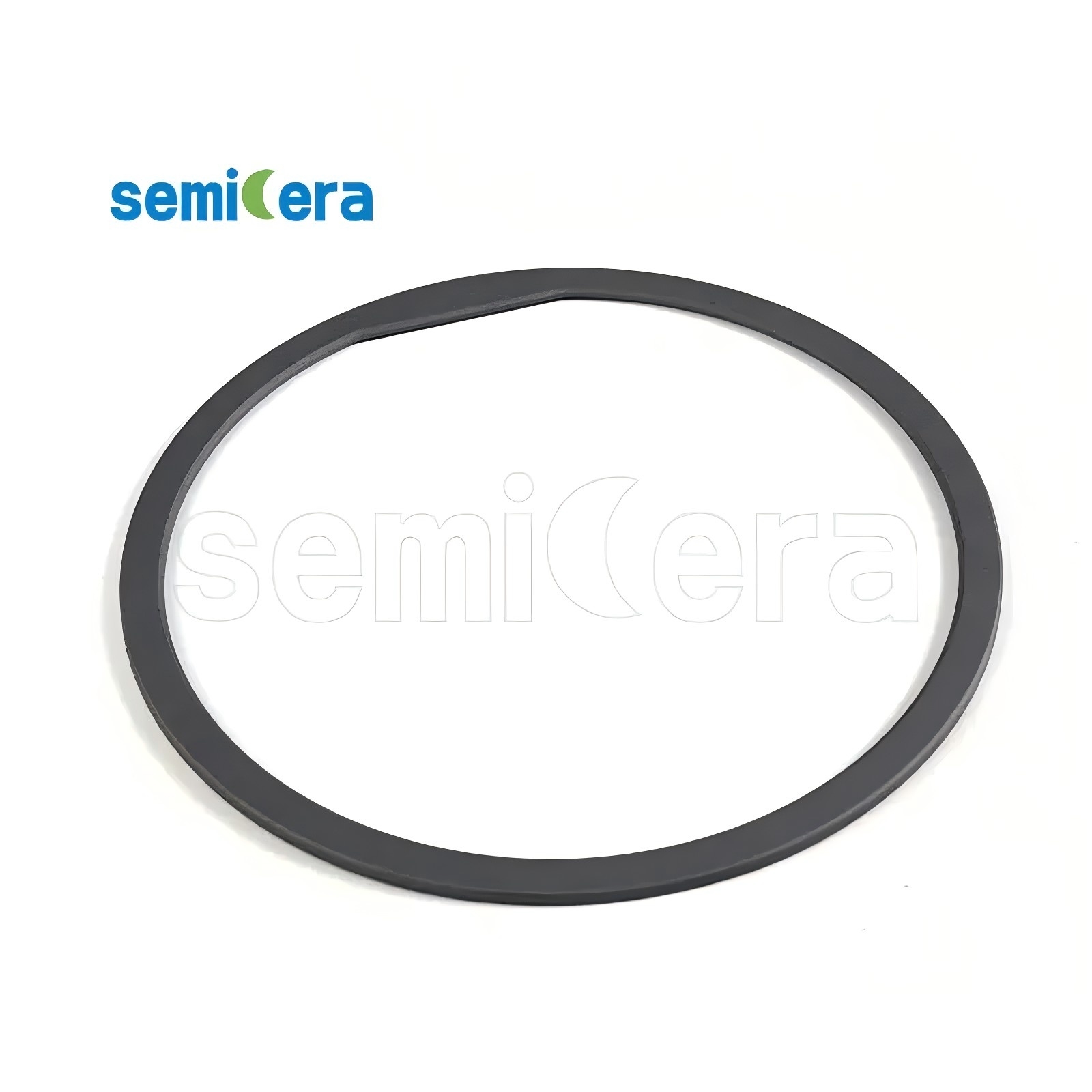
Figure 2: A CVD SiC etching ring – ultra-pure, certified for use in high-density plasma environments.
The CVD SiC coating graphite carrier (model CVD-01) is a key component for MOCVD susceptors. Its material parameters – coating thickness (typ. 100 µm, range 50–150 µm), hardness 2500 Vickers (40 GPa), crystal structure FCC β-phase (111) orientation – are all verified under Semicera's ISO 9001 system. When you order this product, you can request the certificate of conformance that ties each batch to the quality management system.
Comparison with OEM Parts
A common buyer concern is whether certified aftermarket materials can match OEM performance. According to Semicera's comparative tests, their SiC/TaC coated parts achieve 10-15% better epitaxial layer uniformity and less than 5% particle generation versus OEM, while costing 30-40% less. The maintenance interval is identical to OEM components. This is only possible because their manufacturing processes are ISO-certified and their purity levels meet or exceed OEM specs.
Step-by-Step Checklist for Buyers
- Step 1: Identify which process step (epitaxy, annealing, etch, crystal growth) requires new materials.
- Step 2: Shortlist suppliers with published ISO 9001, 14001, and 45001 coverage for your product category.
- Step 3: Request individual product data sheets. For example, the SiC wafer boat (model SiC-01) should list material substrate (SiSiC or RSiC), max working temp (1600°C), and lifespan >5× quartz.
- Step 4: Verify the supplier's quality control tests. Semicera performs 100% inspection before shipment, including dimensional measurement, purity analysis (ICP-MS), and thermal cycle screening.
- Step 5: Check delivery and payment terms. Semicera offers MOQ of 1 unit, 100% T/T in advance for new customers, and delivery methods EXW/FCA/DAP/DDP.
Real-World Use Cases
Case 1: North America – 900 units/month for epitaxy
A major US fab replaced its OEM SiC wafer boats (model SiC-01) and furnace tubes (model SiC-02) with Semicera's certified alternatives. After 2 years of continuous operation, they achieved stable mass production with consistent epitaxial uniformity and a 15% reduction in maintenance downtime. The high-density CVD coating and strict dimensional tolerances were key.
Case 2: Asia-Pacific – 200 units/month for epitaxy
A Japanese manufacturer adopted Semicera's SiC wafer boats and paddles (model SiC-03). With ultra-low particle counts, overall wafer yield increased by 2.5%. The customer highlighted the consistent coating thickness and excellent thermal conductivity as decisive factors.
Case 3: Europe – 10,000 units/year for SiC crystal growth
A German SiC substrate manufacturer uses Semicera's CVD SiC coating graphite carriers (model CVD-01) and CVD SiC particles (model CVD-04) as raw material for PVT growth. After two years, they reported consistent crystal quality and 15% less process downtime compared to previous suppliers. The ultra-high purity (6N+) matrix coating eliminated outgassing issues.
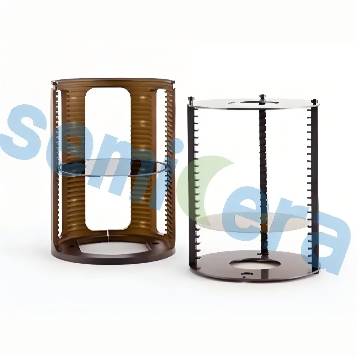
Figure 3: A SiC wafer boat from Semicera – ISO 14001 and ISO 45001 certified for diffusion processes.
Frequently Asked Questions (FAQ)
Q1: Does Semicera hold ISO 9001 certification?
Yes. Semicera's semiconductor graphite product (ID 4932) is ISO 9001 certified, covering quality management for the global market. The certificate is valid until December 1, 2026.
Q2: How can I verify that the CVD SiC coating graphite carrier meets 6N purity?
You can request the batch-specific analysis report. Semicera's standard for CVD-01 is total ash ≤ 5 ppm, equivalent to 99.99995% purity. Independent third-party lab results are available upon request.
Q3: What certifications apply to quartz furnace tubes?
Quartz furnace tubes (model quartz furnace tube) from Semicera are covered under the company's ISO 9001 scope. The material spec (OH < 20 ppm, OD tolerance ±1%) ensures consistency. For environmental compliance, the entire facility operates under ISO 14001.
Q4: Do you provide a certificate of analysis for each shipment?
Yes. Semicera issues a certificate of conformance (CoC) with every order, including purity data, dimensional measurements, and certification status. Pre-shipment testing is standard.
Q5: What is the minimum order quantity for certified semiconductor graphite?
MOQ is 1 unit, which allows you to evaluate the material before committing to volume. Payment terms: 100% T/T in advance for new customers; 70/30 for long-term partners.
Conclusion: Partner with a Certified Supplier
Sourcing semiconductor process materials from a certification-compliant supplier is the only way to protect your fab's yield and reliability. By demanding ISO 9001, 14001, and 45001 certifications alongside material-specific purity data, you eliminate guesswork and reduce risk. Semicera has demonstrated compliance across its entire portfolio — from high-purity graphite and CFC materials to CVD SiC coatings and etch rings — serving customers in over a dozen countries.
To start your vendor qualification process, download the full product catalog below for detailed specifications and certification documents.
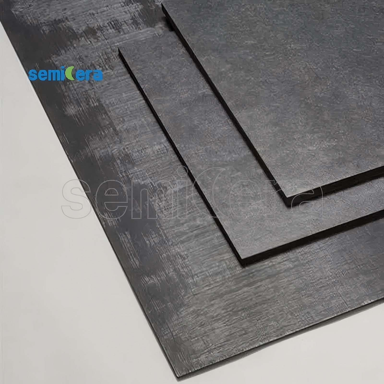
Figure 4: CFC material (carbon-carbon composite) – a certified hot-zone component for SiC crystal growth furnaces.