How to Choose the Right Semiconductor Process Material Supplier
How to Choose the Right Semiconductor Process Material Supplier
In advanced semiconductor manufacturing, the purity and consistency of process materials directly determine wafer yield, device performance, and production cost. From epitaxy process materials like MOCVD susceptors to annealing process materials such as SiC wafer boats, and etch process materials including focus rings – every component must meet stringent contamination and dimensional specifications. Yet with dozens of suppliers claiming “ultra-high purity,” how do procurement managers separate reliable partners from marketing claims?
This guide provides a structured framework for evaluating semiconductor process material suppliers. We will define the key material categories, explain the critical performance parameters, and walk through a step-by-step decision process – using real-world examples from a leading manufacturer, Semicera (Ningbo Miami Advanced Material Technology Co., LTD).
What Are Semiconductor Process Materials?
Semiconductor process materials refer to the high-purity consumables and structural components used inside wafer fabrication equipment. They include coated graphite parts, quartzware, silicon carbide ceramics, carbon-fiber composites, and insulation felts. These materials must withstand extreme temperatures (up to 2500 °C), corrosive gas environments (NH₃, H₂, CF₄), and rapid thermal cycling while contributing zero particles or metal contamination.
Key categories include:
- CVD SiC coating graphite carriers – used as susceptors in MOCVD and RTP processes.
- CVD TaC coating graphite carriers – for ultra-high temperature (≥2000 °C) epitaxy with aggressive NH₃/H₂ gases.
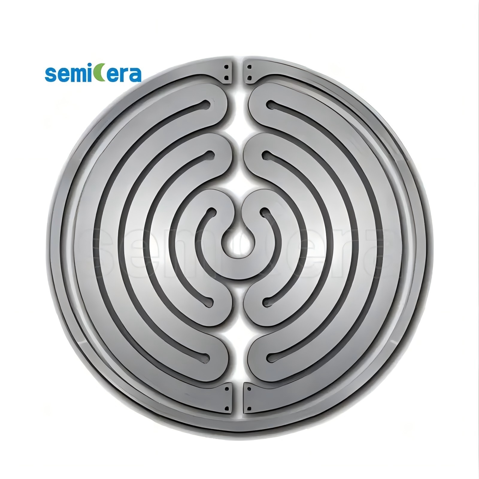
- CVD solid SiC parts – bulk SiC etch rings, dummy wafers for plasma etchers.
- SiC wafer boats and furnace tubes – replace quartz in diffusion/oxidation with >5× lifespan.
- High-purity graphite and CFC materials – hot-zone heaters, crucibles, rigid felt insulation.
- Quartz parts – tubes, boats for lower-temperature processes.
Why Supplier Selection Matters: The Cost of Poor Materials
Choosing the wrong supplier can lead to:
- Yield loss – particle shedding or metal outgassing ruins wafer batches.
- Unplanned downtime – premature cracking or coating peeling forces tool shutdown.
- Process drift – inconsistent thermal properties cause non-uniform deposition or etching.
- Hidden cost – frequent replacement negates any initial price advantage.
Industry fact: A single particle contamination event in a 300 mm fab can scrap an entire lot worth thousands of dollars. Ultra-high purity materials with ash content ≤5 ppm are now the baseline for mainstream nodes.
Key Evaluation Criteria for Semiconductor Process Material Suppliers
1. Material Purity and Trace Impurity Control
For semiconductor graphite, Semicera specifies ash content ≤5 ppm (ultra-pure grade) and ultra-fine grain size of 2–5 µm. For CVD SiC coating, the purity reaches 99.99995 % (6N grade) with total metals <5 ppb for etch ring applications. Always request ICP-MS data for metal contamination per element.
2. Coating Integrity and Thermal Cycling Stability
Delamination of SiC or TaC coatings under thermal shock is a common failure. Semicera performs high-temperature simulation tests and thermal cycle screening to eliminate defective products (see Risk Control practices). A good supplier will share cross-section SEM images and adhesion test results.
3. Dimensional Precision and Surface Quality
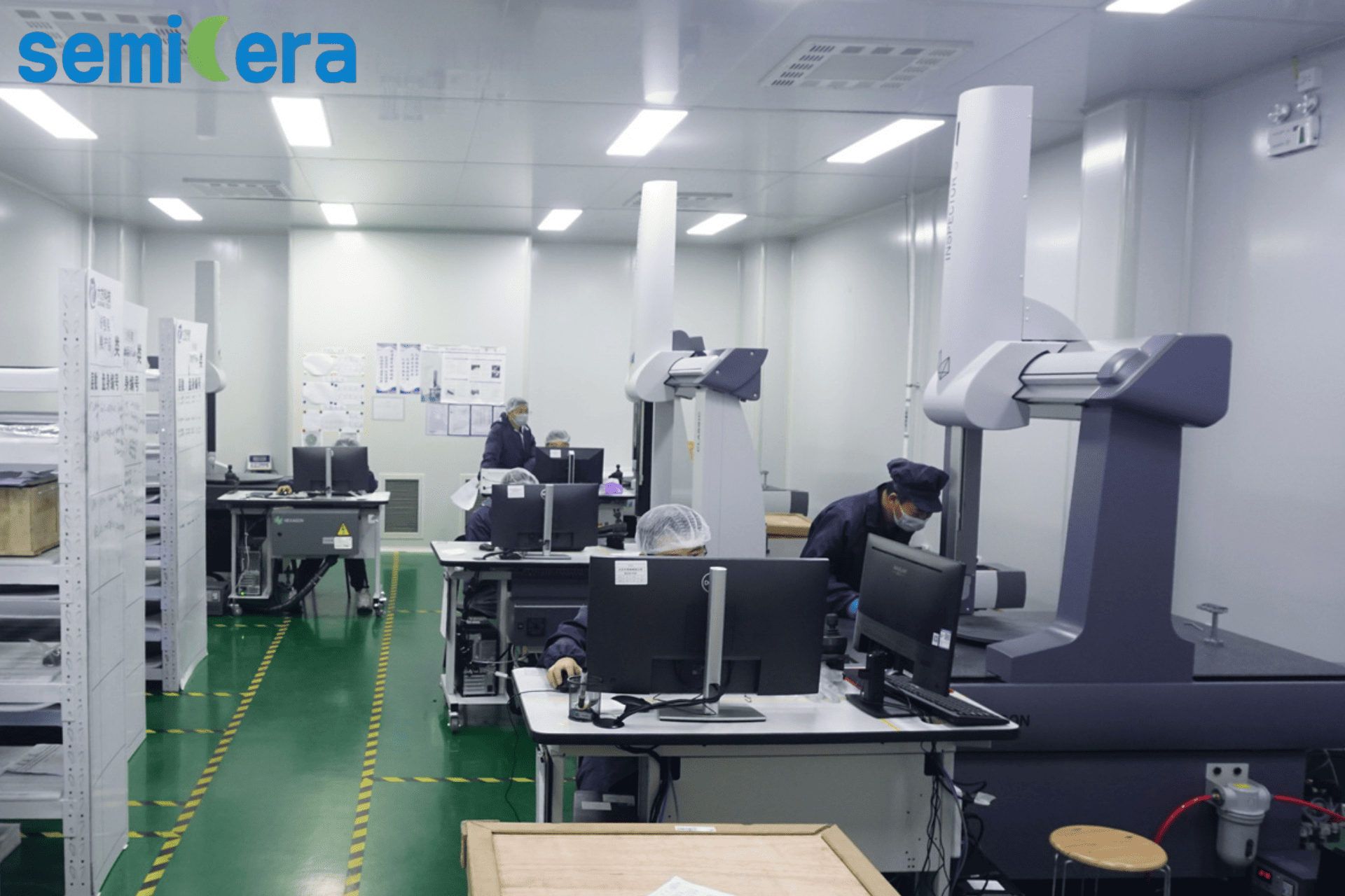
Slot pitch tolerance for SiC wafer boats must be ≤±0.05 mm; etch rings require flatness ≤10 µm. Surface defects like pits or scratches become particle sources. Inspect incoming quality reports and request OGP (optical gaging) data.
4. Manufacturing Capacity and Quality System
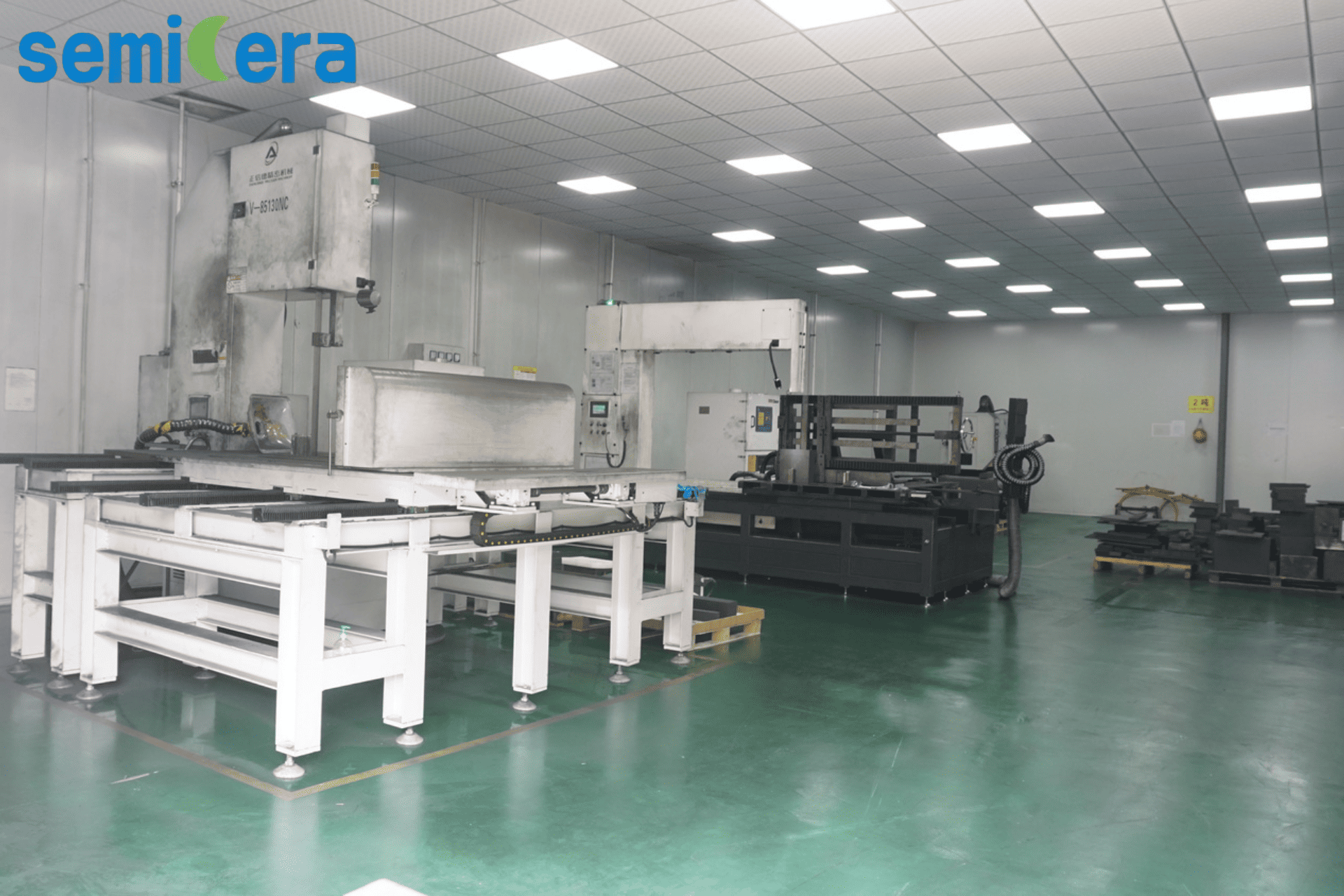
Semicera operates a 40,000 m² facility with 50+ advanced production lines, dual R&D centers, and ISO 9001/ISO 14001/ISO 45001 certified management systems. A monthly capacity of 10,000+ units and a lead time of 30–50 days ensures supply stability for both pilot and volume production.
5. Proven Application Cases
Real-world references reduce risk. Below are selected Semicera case studies:
| Region | Product | Volume | Result |
|---|---|---|---|
| North America | SiC wafer boat, furnace tube, paddle | 900 units/month | 15% less maintenance downtime |
| Japan (APAC) | SiC wafer boat, furnace tube, paddle | 200 units/month | 2.5% wafer yield increase |
| South Korea | CVD SiC/TaC coated carriers, solid SiC parts | 500 pcs/month | 20% reduced edge ring replacement |
| Europe | CVD SiC coating carrier + TaC carrier + CVD SiC particle | 10,000 units/year | 15% process downtime reduction |
6. Total Cost of Ownership (TCO) Comparison
The initial purchase price is only part of the equation. Semicera’s CFC material hot-zone components achieve up to 50% energy saving compared to solid graphite, and SiC-coated parts provide 3–5× longer service life than OEM equivalents. Even with a similar upfront cost, the extended lifespan and improved epitaxial layer uniformity yield a 30–40% lower TCO versus conventional suppliers.
7. Customer Support and Flexibility
Suppliers offering OEM/ODM customization, low MOQ (1 unit), and flexible delivery terms (EXW/FCA/DAP/DDP) are valuable for pilot projects. Semicera also provides remote after-sales support and pre-shipment testing for every order.
Step-by-Step Supplier Selection Process
- Define your process requirements – Identify the tool type, temperature range, gas chemistry, and critical dimension tolerances.
- Shortlist suppliers – Focus on those with proven expertise in your specific process (e.g., MOCVD, RTP, plasma etch).
- Request technical datasheets and certificates – Compare purity, coating thickness, thermal conductivity, mechanical strength.
- Audit the manufacturing facility – Verify raw material sourcing, coating equipment, inspection capabilities, and quality certifications.
- Ask for reference cases – Look for similar applications (same tool model and wafer size) with documented yield improvement.
- Evaluate total cost – Include lifespan, energy savings, maintenance impact, and scrap reduction.
- Run a qualification batch – Start with a small MOQ, test in your process, and monitor performance over several thermal cycles.
Frequently Asked Questions (FAQ)
A: Request the ash content test report (ASTM C561). For semiconductor grade, ask for ≤5 ppm total ash and individual metal analysis via GDMS or ICP-MS.
A: Semicera offers 30–50 days for custom designs, and 1 unit MOQ is available for qualification. Standard products can be shipped within 15–20 days.
A: Yes. Semicera’s CVD TaC coating (model CVD-02) is engineered for ultra-high temperature epitaxy and shows outstanding resistance to ammonia and hydrogen etching up to 2200 °C.
A: For first-time orders, Semicera requires 100% T/T in advance. For long-term cooperation partners, the terms are 70% T/T in advance, 30% before shipment.
A: Yes, 100% of products undergo dimensional inspection, visual inspection, and thermal cycle testing before shipment. A formal QA report is provided.
Conclusion: Build a Reliable Supply Chain with Semicera
Selecting the right semiconductor process material supplier is a strategic decision that affects your fab’s productivity, quality, and cost structure. By focusing on proven purity specifications, coating integrity, manufacturing scale, and real customer outcomes, procurement teams can mitigate risk and unlock long-term value.
Semicera (Ningbo Miami Advanced Material Technology Co., LTD) has been serving global semiconductor leaders since 2015 with a comprehensive portfolio covering CVD SiC/TaC coatings, SiC ceramics, quartz, graphite, and carbon-fiber composites. With ISO-certified production, 600+ experienced staff, and a track record of 10,000+ units shipped annually to Europe, USA, and Asia, Semicera offers the reliability you need.
Download the Product Catalog
Get complete specifications, case studies, and ordering information in our 2025 catalog.
📘 Download PDFOr contact Frank: sales05@semi-cera.com | WhatsApp: +86 15957878134