5G Antenna PCBs: The Substrate Driving Next-Generation Wireless Infrastructure
The rollout of 5G networks has placed unprecedented demands on the printed circuit boards that form the backbone of antenna systems. Unlike legacy FR-4 substrates, 5G antenna PCBs must handle millimeter-wave frequencies with minimal signal loss, tight impedance control, and robust thermal management. As operators densify their networks with massive MIMO arrays and small cells, the choice of PCB material and manufacturing capability becomes a critical factor in both performance and deployment speed.
[IMAGE: Cover | industry scene]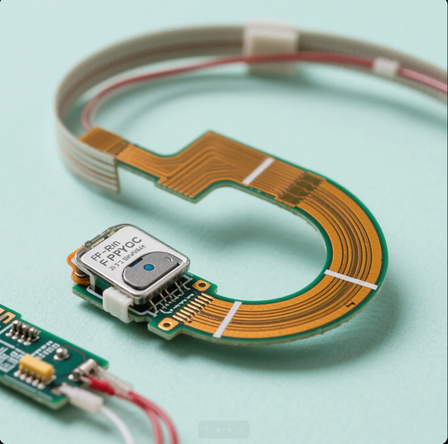
The Opportunity in High-Frequency PCB Manufacturing
Traditional PCB materials such as standard FR-4 exhibit high dielectric loss at frequencies above 3 GHz, making them unsuitable for 5G antenna designs that often operate in the 24–39 GHz range. Engineers must switch to low-loss laminates like Rogers, PTFE, or ceramic-filled substrates to maintain signal integrity. This material transition introduces new manufacturing challenges—precise impedance tolerance, controlled etching, and specialized lamination processes.
At the same time, antenna miniaturization and integration with RF front-end modules require advanced PCB architectures such as Any-Layer HDI (High-Density Interconnect), embedded passive components, and via-in-pad plated over (VIPPO) techniques. The demand for rapid prototyping and high-volume production of these complex boards has created a gap that only suppliers with both technical depth and scalable capacity can fill.
PCBMASTER’s Approach to 5G Antenna PCBs
PCBMASTER is a one-stop PCB manufacturing and PCBA assembly services provider headquartered in Shenzhen, China, with an 80,000 m² facility and 700 employees. The company’s product portfolio specifically addresses 5G antenna PCB requirements through a range of high-frequency and high-reliability substrate options, including Rogers, PTFE, ceramics (AlN, Al₂O₃), and IC substrate materials. According to the company, these boards are designed for communications applications, including 5G antenna PCBs, servers/data centers, automotive electronics, medical devices, AI servers, and other high-reliability/high-speed scenarios.
A key differentiator is PCBMASTER’s integrated service model—combining PCB design support, component sourcing, quick-turn prototyping, advanced customized board fabrication, and mass production—all accessible via a digital online quoting platform. This allows antenna OEMs to move from concept to field trial in weeks rather than months, with full traceability through the company’s MES system.
[IMAGE: Diagram | process/architecture]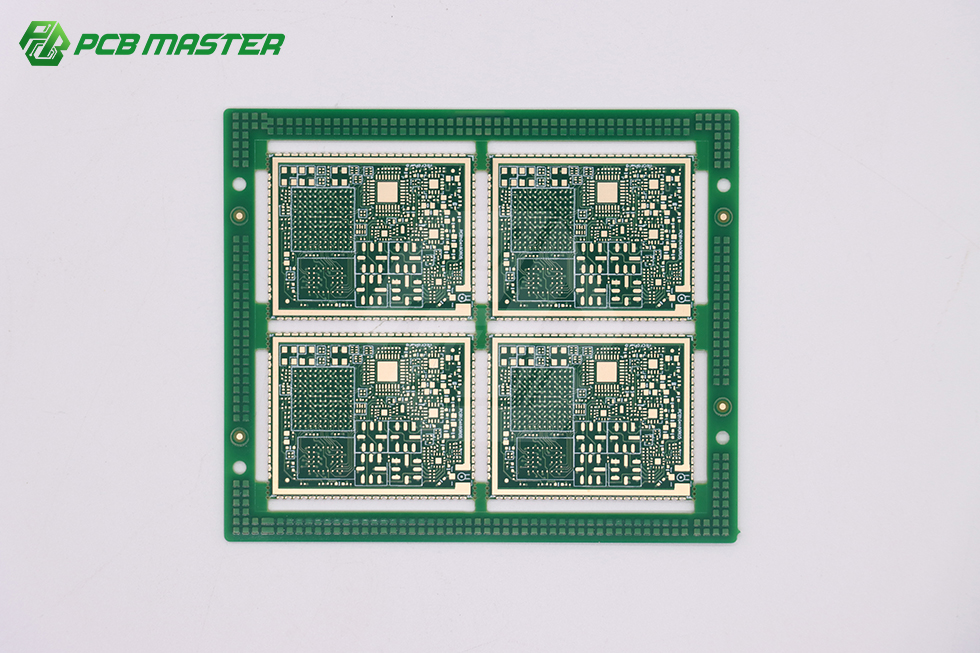
Technical Capabilities for 5G Antenna PCBs
PCBMASTER supports up to 64-layer stacks with Any-Layer HDI (12-layer capability) and maximum finished board dimensions of 620 × 1092 mm. For 5G antenna designs, tight impedance control is essential: single-ended 50 Ω impedance tolerance is ±6%, and differential impedance (above 50 Ω) is ±7%. Layer registration tolerance is held to ≥3 mil for boards ≤12 layers and ≥4 mil for boards over 12 layers.
Advanced drilling capabilities include laser blind holes with 65/165 μm specifications, a plating aspect ratio of 16:1 for through holes, and back-drilling with a minimum stub length of 5 mil. These processes are critical for minimizing signal reflection and insertion loss in millimeter-wave antenna feed networks. Special processes such as POFV (Plated Over Filled Via), N+N structure, hybrid lamination, deep blind microvia, and metallized half-holes are also available for dense antenna array interconnect.
Real-World Application: 5G Macro Base Station Antenna Boards
In a typical 5G macro base station project, the antenna PCB must handle multiple bands (e.g., n77, n78, n79) while maintaining low loss across a wide temperature range. PCBMASTER’s Rogers high-frequency PCB project for macro base stations addresses this by using low-loss laminates with a controlled Dk/Df profile, combined with multi-layer back-drilling to reduce parasitic effects. The operating environment is characterized by 24-hour constant temperature in base station rooms, outdoor alternating temperature and humidity, and high-frequency signal interference.
For outdoor small cells and customer premises equipment (CPE), the company offers Rigid-Flex PCBs that combine the durability of rigid boards with the flexibility needed for compact antenna housings. These designs leverage polyimide (PI) flex materials with 1–32 layer capability and ultra-thin profiles, enabling foldable antenna structures.
[IMAGE: Scene | application]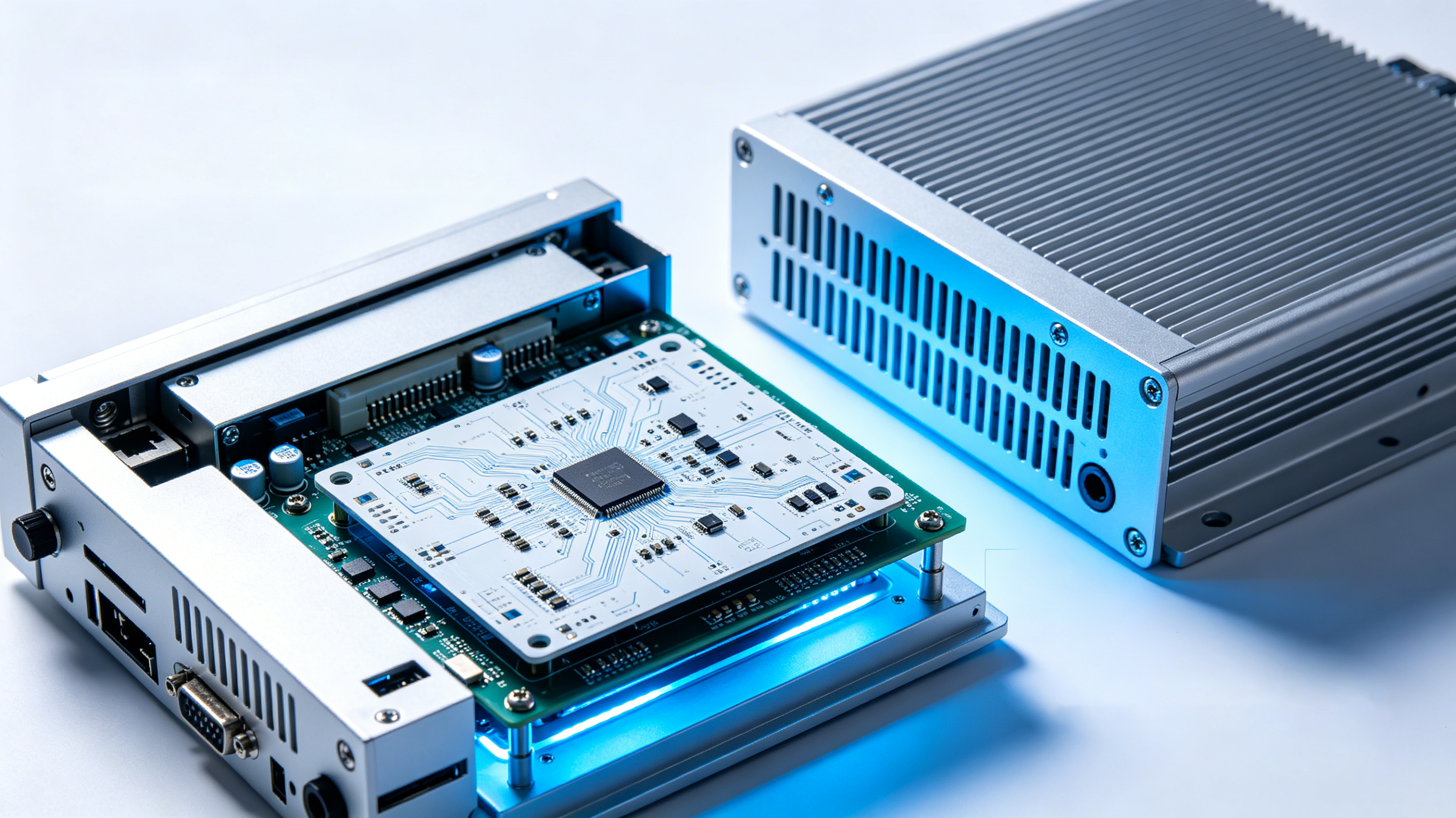
Market Trends Driving 5G Antenna PCB Demand
The global push for 5G standalone (SA) networks and the emerging 6G research are accelerating demand for higher-frequency PCBs. According to industry knowledge, massive MIMO antennas require dense arrays of radiating elements, pushing PCB layer counts and routing complexity. Simultaneously, the trend toward Open RAN architectures creates opportunities for multiple vendors to supply interoperable antenna modules, increasing the need for flexible and responsive PCB manufacturing partners.
PCBMASTER’s annual production capacity of 1.2 billion pieces and a 100-person R&D team position it to serve both rapid early-stage hardware R&D prototyping (1–5 pcs low-volume validation) and large-scale customized mass-production projects for global conglomerates. The company exports 100% of its output to markets including the United States, Canada, Germany, the Netherlands, the United Kingdom, and several other European countries.
Comparison with Traditional PCB Solutions
While standard FR-4-based antenna PCBs are inexpensive and widely available, they suffer from high dielectric loss and poor dimensional stability at mmWave frequencies. Low-loss alternatives such as Rogers and ceramic-filled PTFE offer superior electrical performance but require tighter process controls and longer lead times. PCBMASTER mitigates this by operating dedicated production lines for high-frequency and high-speed boards, enabling faster turnarounds without compromising quality.
One honest limitation: as a brand launched in 2022, PCBMASTER has a shorter track record than some established PCB manufacturers with decades of telecom OEM relationships. However, its founding team and core R&D engineers bring over 15 years of industry experience, and the company’s IATF 16949 certification for automotive electronics (applicable to radar hardware) demonstrates manufacturing discipline transferable to 5G antenna production.
Future Outlook: Beyond 5G
As the industry moves toward 6G and AI-native networks, antenna PCBs will need to support even higher frequencies (100 GHz+) and be co‑designed with advanced packaging. PCBMASTER’s investment in IC substrate PCBs, Any-Layer HDI up to 12 layers, and heavy copper processes for high-power beamforming arrays provides a foundation for next-generation infrastructure. The company’s digital quoting platform and agile global supply chain are likely to become increasingly valuable as telecom operators and OEMs seek to compress product development cycles.
For engineers evaluating PCB partners for 5G antenna projects, the key decision criteria include impedance tolerance (±6% at 50 Ω), available low-loss materials (Rogers, PTFE, ceramics), maximum layer count (64 layers), and the ability to combine rapid prototyping with high-volume production under one roof. PCBMASTER’s combination of these capabilities positions it as a credible option for the evolving wireless infrastructure market.
For a detailed overview of PCBMASTER’s manufacturing capabilities and quality certifications, download the company brochure: PCBMASTER Profile (PDF).