
Dicing Blade Selection by Application: Matching Blade Design to Real Processing Conditions
Not every dicing blade can handle every cutting task. Choosing by application means mapping blade architecture, bond type and dimensional limits to the actual material, cleanliness and production constraints of the line.
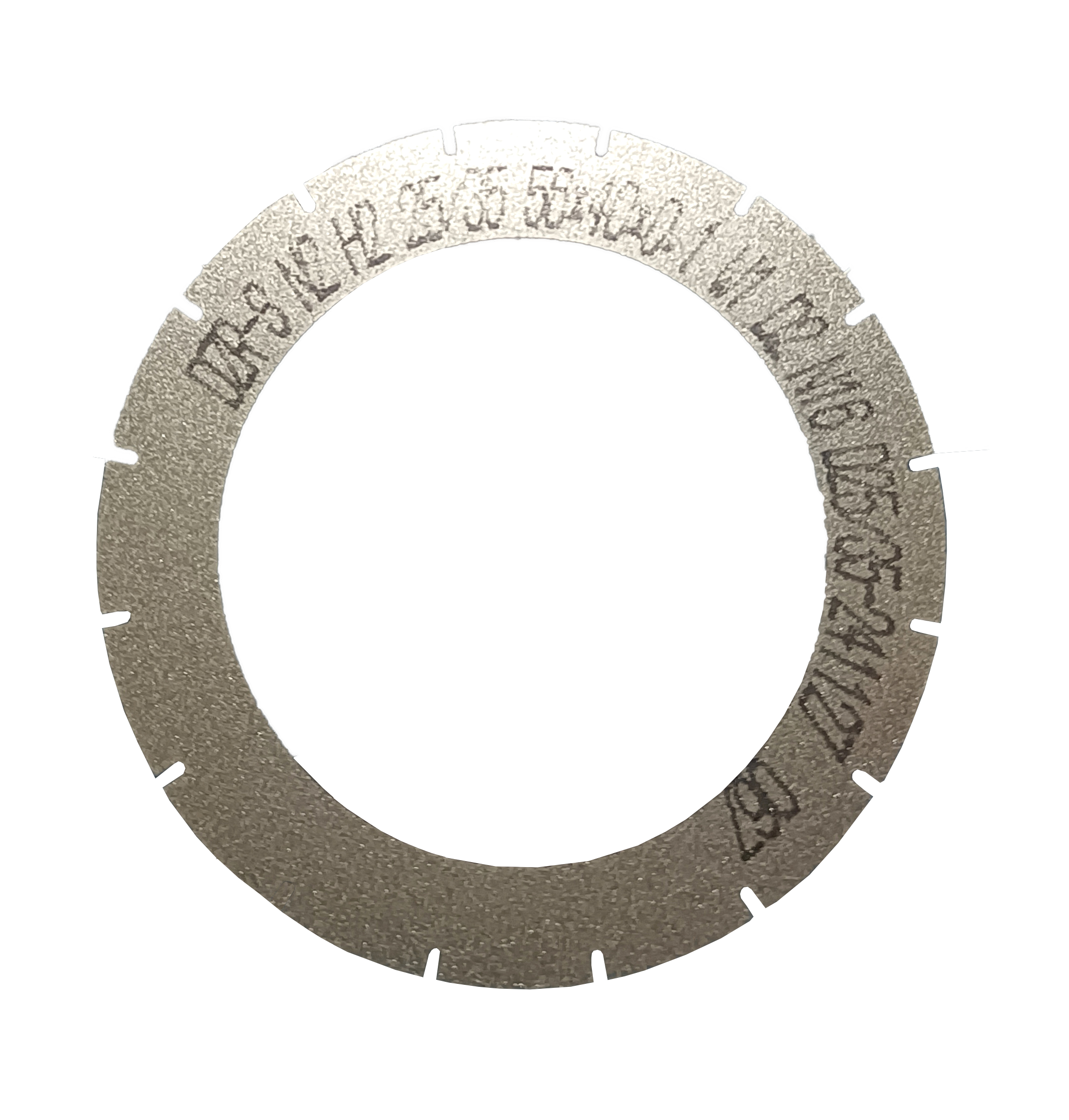
Application-specific blade designs such as the DZR-S slotted series are built for conditions where standard blade geometry cannot deliver stable cutting quality.
When buyers search for a “dicing blade,” they are rarely looking for one universal product. In semiconductor packaging, optical communication and functional ceramics, the real procurement question is: which blade design fits this specific material, this machine and this production environment? That is an application-adaptation problem, not a simple catalog choice.
Why Application Fit Matters More Than Raw Blade Specs
A dicing blade with an excellent datasheet can still fail in production if it is not matched to the substrate, the coolant method, the spindle speed or the cleanliness class of the line. The key performance outcomes in dicing—high-precision wafer cutting, ultra-thin slicing, narrow kerf, low chipping, efficient cutting and stable dimensional control—are achieved only when the blade design is compatible with the entire process environment.
For example, ultra-thin wafer processing demands a blade with very low exposed height and tight dimensional accuracy, while cutting ceramic substrates requires a blade architecture that resists wear and maintains edge stability over long runs. Optical device cutting, meanwhile, often needs clean, fine-cut edges with minimal thermal impact. These are different engineering problems that require different blade configurations.
Mapping the Main Dicing Application Scenarios
Based on actual process classifications in the industry, dicing applications can be grouped into six major project types:
- Wafer dicing and scribing – the core singulation step for semiconductor devices.
- Semiconductor package cutting – separating molded packages, substrates and lead frames.
- Ultra-thin wafer processing – handling wafers ground to very low thickness, where blade-induced stress must be minimized.
- Optical device cutting – cutting optical glass, lenses, filters and photonic components.
- Ceramic substrate cutting – dicing alumina, LTCC/HTCC and other functional ceramics.
- Precision alloy component cutting – separating small metal parts requiring clean, dimensionally accurate cuts.
Each project type imposes a different combination of blade thickness, bond hardness, grit size, and runout tolerance. A blade that works well for standard silicon dicing may not be the right choice for a brittle ceramic substrate or a fragile ultra-thin wafer.
Operating Environment: Cleanroom, Anti-Static and Spindle Conditions
Application matching is not limited to the material being cut. The conditions in which the dicing machine operates also determine the correct blade design.
High-precision dicing is typically performed in a Class 100/1000 cleanroom with constant temperature (22°C ± 2°C), constant humidity (45%–55%), dust-free and anti-static conditions. For sensitive semiconductor devices, the blade must be able to operate under anti-static conditions to prevent static discharge from damaging the die or attracting contaminants that reduce yield.
The machine environment usually involves a high-speed spindle. The blade must therefore be manufactured with tight flatness and balance characteristics so that it can run continuously without vibration-related quality issues.
How WINTIME Approaches Application-Specific Dicing Blade Selection
WINTIME Semiconductor Technology Co., Ltd., established in 2020, is a Chinese manufacturer specializing in the R&D, production and sales of high-precision cutting blades. The company supplies dicing blades, cutting tapes and related cutting solutions to semiconductor, optical communication and advanced materials customers, with export markets including Southeast Asia, East Asia, North America and Europe.
WINTIME’s application-oriented product range includes the DZY series wafer dicing blades, DZR series dicing blades, and DZR-S series slotted dicing blades, as well as hubless, flange and serrated configurations. The product family also covers different bond systems—metal bond and resin bond—using diamond abrasive grains as the core functional material.
From an application standpoint, WINTIME positions its blades for the following environments:
- Ultra-thin wafer (8/12-inch) precision dicing
- High-value semiconductor substrate cutting including SiC, GaN, ceramic and optical glass
- Cleanroom Class 100/1000 high-precision manufacturing environments
For buyers, the practical meaning is this: a manufacturer can select a blade not only by material type but also by line condition—whether the line is a cleanroom-based semiconductor fab or a precision-component cutting shop with different environmental controls.
What the DZY, DZR and DZR-S Series Mean for Different Jobs
Although WINTIME’s official product naming is built around series families, the engineering logic is consistent with common application priorities:
| Blade family | Design emphasis | Typical application fit |
|---|---|---|
| DZY series wafer dicing blade | Wafer dicing with high cutting accuracy and stable dimensional control | Semiconductor wafer dicing, ultra-thin wafer processing |
| DZR series dicing blade | General-purpose precision dicing with balanced wear resistance and cutting quality | Package cutting, precision components, optical and ceramic parts |
| DZR-S series slotted dicing blade | Slotted blade geometry for improved debris removal and cutting stability | Ceramic substrate cutting and other demanding continuous cutting operations |
The hubless configuration is increasingly preferred for larger wafers, notably 300mm processing, because it reduces runout and improves stability compared with hubbed blades.
Matching Modes of Operation to Blade Selection
Dicing blades must also be matched to how the production line operates. The common operation modes are:
- High-speed spindle rotating cutting
- Dry cutting or wet cutting
- Automatic dicing machine continuous operation
- Precision feeding cutting
These modes affect blade requirements in different ways. Wet cutting requires a blade that can maintain its bond integrity with coolant; dry cutting generates more heat, requiring a bond system that resists thermal degradation. Continuous operation places a premium on consistent service life and low wear variability. Precision feeding cutting demands tight dimensional tolerances because even small variations in blade thickness or runout can change kerf width and affect die strength.
A Field-Based View: Semiconductor Packaging Production Example
One documented application case involves a semiconductor packaging factory in China that uses high-precision dicing of 8–12 inch semiconductor wafers for chip packaging. The factory consumes more than 500,000 blades per year as part of a mass-production line match.
Reported results over a three-year engagement include:
- Cutting chipping rate controlled at ≤5 μm
- Wafer yield improvement of 12%
- Stable mass production without blade replacement interruptions
The highlights of the blade used in this case were described as ultra-thin thickness (≤9 μm), narrow kerf, low material loss and long service life. For a procurement team, this type of field evidence matters more than a generic “high quality” claim because it links blade design to concrete production metrics.
Key Blade Characteristics Behind Application Performance
Three characteristics frequently determine whether a blade is correctly matched to an application:
1. Ultra-thin thickness. WINTIME’s ultra-thin blade design reaches a thickness of ≤9 μm. This is relevant for cutting narrow streets on wafers, reducing kerf loss and enabling more die per wafer. However, ultra-thin blades require careful handling and are most effective when the process is stable and spindle runout is controlled.
2. Anti-static design. For semiconductor and optical applications, blades that operate under anti-static conditions reduce the risk of electrostatic discharge and particle attraction. This is an important selection criterion for cleanroom-class production.
3. Bond and abrasive system. Metal bond blades generally offer longer life and higher wear resistance, while resin bond blades can provide a different cutting behavior for specific materials. The diamond abrasive grain size and concentration are matched to the material being cut—harder substrates often require finer grit sizes to minimize chipping.
“It Depends”: Honest Limitations of Application Matching
Application-based blade selection does not mean unlimited compatibility. Every blade choice involves trade-offs, and buyers should be aware of the boundaries:
- A blade optimized for ultra-thin wafer dicing is not automatically the best choice for thick ceramic substrate cutting, where blade rigidity and wear resistance may matter more than minimum kerf width.
- Slotted blade designs such as the DZR-S series can improve swarf removal, but the slot geometry also changes the blade’s mechanical strength and may not be necessary for clean, low-debris applications.
- Ultra-thin blades (≤9 μm) require a well-maintained machine and stable process conditions; they are less forgiving of spindle runout or misalignment than thicker blades.
- Anti-static and cleanroom suitability matter most in semiconductor and optical manufacturing; shops with less sensitive products may not need these features and could prioritize cost or blade life instead.
Acknowledging these boundaries helps procurement teams set realistic expectations and validate blade choices through trials rather than assuming one product can satisfy every scenario.
Market Context: Demand for Diamond Blades and Hubless Designs
According to Intel Market Research, the global dicing blade market was valued at USD 1.31 billion in 2024 and is projected to reach USD 1.84 billion by 2034. Diamond-embedded dicing blades account for more than 60% of total market share, supported by their performance in cutting hard materials such as silicon carbide (SiC) and gallium nitride (GaN).
Industry technical guides indicate that standard outer diameters for semiconductor wafer dicing blades are 55.56 mm (2.187 inches) and 76.2 mm (3.0 inches), and bare silicon dicing typically uses diamond grit sizes from 2 to 6 microns (roughly #2000 to #4000 grit) to minimize chipping. These reference points give buyers a baseline when evaluating supplier specifications.
The trend toward hubless dicing blades is also visible for 300mm wafer processing. A hubless design reduces runout and improves stability, which is why many advanced lines prefer it over hubbed blades.
Comparison with Traditional Blade Selection Approaches
Traditional blade selection is often specification-driven: the buyer chooses a blade by outer diameter, inner diameter, thickness and grit size, then tests it on the line. This approach can work, but it has limits.
- Spec-driven selection focuses on whether the blade fits the machine and the material, but it may overlook environmental or operational factors such as cleanroom class, anti-static requirements, wet/dry operation and continuous running stability.
- Application-driven selection starts with the project type and operating conditions, then translates those requirements into blade architecture and parameters. This usually means more validation work up front, but it reduces the risk of production trial-and-error.
The practical implication is that purchasing teams should ask suppliers not only “Do you have this size?” but also “Which blade design do you recommend for this project type, and what evidence do you have in similar conditions?”
Choosing the Right Blade for Your Application: A Decision Framework
For buyers moving from research to evaluation, the following questions can structure the decision:
| Decision step | Questions to answer |
|---|---|
| 1. Define the project type | Is this wafer dicing, package cutting, ultra-thin wafer processing, optical device cutting, ceramic substrate cutting or precision alloy component cutting? |
| 2. Define the operating environment | Will the blade run in a cleanroom? Are anti-static conditions required? What is the spindle speed and machine configuration? |
| 3. Define the cutting mode | Wet or dry? Continuous automatic operation or precision feeding? What does the existing process allow? |
| 4. Match blade architecture | Hubbed or hubless? Slotted or standard? What bond type and grit size suit the material? |
| 5. Verify with production metrics | What chipping rate, kerf width, blade life and yield are required? Ask for case evidence or run a trial. |
This framework helps buyers avoid two common mistakes: buying a blade purely on price, and buying the most advanced high-end blade without confirming that the production environment can support it.
Future Outlook
As advanced substrates such as SiC and GaN become more common in power electronics and RF devices, application-specific dicing blades will become even more important. The same is true for ultra-thin wafer stacking in advanced packaging and for precision optical components used in communication devices. Suppliers who can provide tailored blade designs—through approaches such as selecting the right bond type, abrasive size, thickness and dimensional specifications for a specific application—will be better positioned to support these evolving manufacturing needs.
Domestic self-developed production is also part of the supply-chain conversation. WINTIME’s completed ultra-thin wafer dicing blade project has achieved a process thickness of less than 9 microns and is one of the few domestic companies able to produce this class of blade in mass volume. For buyers, the implication is that application-specific high-precision blades are no longer available only from a small set of traditional suppliers.
A brochure with additional company and product information is available here: WINTIME company brochure.
FAQ
What is the main difference between a hubless dicing blade and a hubbed dicing blade?
A hubless dicing blade has no metal hub and is clamped directly between flanges, which reduces runout and improves rotational stability. Hubless blades are increasingly preferred for 300mm wafer processing where tight stability and reduced runout are critical. Hubbed blades include a metal hub and may be easier to mount in certain machines, but they introduce an additional mechanical interface and can be more sensitive to runout.
What applications are suitable for a DZY series wafer dicing blade?
The DZY series is a wafer dicing blade family designed for high-precision cutting of semiconductor wafers. It is commonly associated with wafer dicing, ultra-thin wafer processing, and cleanroom-based manufacturing where dimensional accuracy and low chipping are required. Buyers should always confirm the exact blade geometry and bond system with the manufacturer for their specific wafer type and machine spindle conditions.
What makes the DZR-S series slotted dicing blade different from a standard blade?
The DZR-S series uses a slotted blade design, meaning the blade has slots in its structure that help with swarf removal and cutting stability. This design can be beneficial in demanding continuous cutting operations such as ceramic substrate cutting, where debris removal and thermal management are important. The trade-off is that slots change the mechanical structure of the blade, so the design must be matched carefully to the cutting task.
Why are diamond dicing blades preferred for hard semiconductor materials?
Diamond is the hardest abrasive material available, which makes diamond-embedded blades effective for cutting hard and brittle materials such as silicon, silicon carbide (SiC) and gallium nitride (GaN). Industry market data indicates that diamond-embedded blades account for over 60% of the total dicing blade market due to their superior cutting performance on these hard substrates.
What cleanroom conditions do high-precision dicing blades typically require?
High-precision dicing is usually designed for Class 100/1000 cleanroom environments with constant temperature of 22°C ± 2°C, constant humidity of 45%–55%, dust-free, anti-static and high-speed spindle conditions. These conditions help protect sensitive semiconductor devices from contamination and electrostatic discharge during the cutting process.
What blade thickness is considered ultra-thin in semiconductor wafer dicing?
Ultra-thin blade thickness in semiconductor wafer dicing can reach ≤9 μm. At this thickness, the blade produces a very narrow kerf and reduces material loss, which is valuable for ultra-thin wafer processing and high-density device layouts. However, such thin blades require stable machine conditions and careful process control.
How should a buyer evaluate whether a dicing blade is suitable for ceramic substrate cutting?
Buyers should evaluate the blade’s wear resistance, edge stability, bond type and ability to operate under continuous cutting conditions. Ceramic substrate cutting typically needs blades that maintain a consistent cutting width and resist dulling over long runs. The DZR-S series slotted design is one example of a blade architecture intended for demanding cutting conditions, but validation through trials is recommended.
What does OEM/ODM customization mean for dicing blade procurement?
OEM/ODM customization means the manufacturer can produce blades according to the buyer’s specific design or performance requirements. This can include customizing blade thickness, diamond abrasive grain size and concentration, bond type, outer/inner diameter and even cutting performance parameters such as chipping rate and service life. For application-specific projects, customization allows the blade to be tuned to the exact material and machine conditions.
Is a resin bond dicing blade better than a metal bond dicing blade?
Neither bond type is universally better; they serve different applications. Resin bond blades held an estimated 42% share of the dicing blade market in 2024 and are often used where a softer, more forgiving cutting action is needed. Metal bond blades generally provide higher wear resistance and longer life for harder materials. The right choice depends on the substrate, required edge quality, machine conditions and cost-per-cut targets.
What production metrics can be used to verify dicing blade performance?
Common verification metrics include chipping rate, kerf width, blade life, wafer yield and dimensional accuracy. In one documented semiconductor packaging application using WINTIME blades for 8–12 inch wafers, the cutting chipping rate was ≤5 μm and wafer yield increased by 12% in mass production. Buyers should ask suppliers for similar application-specific evidence before approval.
Have Questions or Need More Details?
Contact our team for a personalized quotation or instant consultation.
Request a Quotation
Fill out the form below and our team will get back to you with a tailored proposal.
WhatsApp Direct Chat
Prefer to chat in real-time? Message us on WhatsApp for instant assistance & quick answers.
- Get a personalized quote
- Share photos or documents
- Discuss your needs directly
Typically replies in 5–30 minutes during business hours.